EP1146617A2 - High-powered semiconductor laser array apparatus - Google Patents
High-powered semiconductor laser array apparatus Download PDFInfo
- Publication number
- EP1146617A2 EP1146617A2 EP01303078A EP01303078A EP1146617A2 EP 1146617 A2 EP1146617 A2 EP 1146617A2 EP 01303078 A EP01303078 A EP 01303078A EP 01303078 A EP01303078 A EP 01303078A EP 1146617 A2 EP1146617 A2 EP 1146617A2
- Authority
- EP
- European Patent Office
- Prior art keywords
- laser array
- laser
- array structure
- oscillation units
- semiconductor laser
- Prior art date
- Legal status (The legal status is an assumption and is not a legal conclusion. Google has not performed a legal analysis and makes no representation as to the accuracy of the status listed.)
- Withdrawn
Links
Images







Classifications
-
- H—ELECTRICITY
- H01—ELECTRIC ELEMENTS
- H01S—DEVICES USING THE PROCESS OF LIGHT AMPLIFICATION BY STIMULATED EMISSION OF RADIATION [LASER] TO AMPLIFY OR GENERATE LIGHT; DEVICES USING STIMULATED EMISSION OF ELECTROMAGNETIC RADIATION IN WAVE RANGES OTHER THAN OPTICAL
- H01S5/00—Semiconductor lasers
- H01S5/40—Arrangement of two or more semiconductor lasers, not provided for in groups H01S5/02 - H01S5/30
- H01S5/4025—Array arrangements, e.g. constituted by discrete laser diodes or laser bar
- H01S5/4031—Edge-emitting structures
- H01S5/4068—Edge-emitting structures with lateral coupling by axially offset or by merging waveguides, e.g. Y-couplers
-
- A—HUMAN NECESSITIES
- A61—MEDICAL OR VETERINARY SCIENCE; HYGIENE
- A61B—DIAGNOSIS; SURGERY; IDENTIFICATION
- A61B18/00—Surgical instruments, devices or methods for transferring non-mechanical forms of energy to or from the body
- A61B18/18—Surgical instruments, devices or methods for transferring non-mechanical forms of energy to or from the body by applying electromagnetic radiation, e.g. microwaves
- A61B18/20—Surgical instruments, devices or methods for transferring non-mechanical forms of energy to or from the body by applying electromagnetic radiation, e.g. microwaves using laser
-
- A—HUMAN NECESSITIES
- A61—MEDICAL OR VETERINARY SCIENCE; HYGIENE
- A61F—FILTERS IMPLANTABLE INTO BLOOD VESSELS; PROSTHESES; DEVICES PROVIDING PATENCY TO, OR PREVENTING COLLAPSING OF, TUBULAR STRUCTURES OF THE BODY, e.g. STENTS; ORTHOPAEDIC, NURSING OR CONTRACEPTIVE DEVICES; FOMENTATION; TREATMENT OR PROTECTION OF EYES OR EARS; BANDAGES, DRESSINGS OR ABSORBENT PADS; FIRST-AID KITS
- A61F9/00—Methods or devices for treatment of the eyes; Devices for putting in contact-lenses; Devices to correct squinting; Apparatus to guide the blind; Protective devices for the eyes, carried on the body or in the hand
- A61F9/007—Methods or devices for eye surgery
- A61F9/008—Methods or devices for eye surgery using laser
- A61F2009/00861—Methods or devices for eye surgery using laser adapted for treatment at a particular location
- A61F2009/00863—Retina
-
- A—HUMAN NECESSITIES
- A61—MEDICAL OR VETERINARY SCIENCE; HYGIENE
- A61F—FILTERS IMPLANTABLE INTO BLOOD VESSELS; PROSTHESES; DEVICES PROVIDING PATENCY TO, OR PREVENTING COLLAPSING OF, TUBULAR STRUCTURES OF THE BODY, e.g. STENTS; ORTHOPAEDIC, NURSING OR CONTRACEPTIVE DEVICES; FOMENTATION; TREATMENT OR PROTECTION OF EYES OR EARS; BANDAGES, DRESSINGS OR ABSORBENT PADS; FIRST-AID KITS
- A61F9/00—Methods or devices for treatment of the eyes; Devices for putting in contact-lenses; Devices to correct squinting; Apparatus to guide the blind; Protective devices for the eyes, carried on the body or in the hand
- A61F9/007—Methods or devices for eye surgery
- A61F9/008—Methods or devices for eye surgery using laser
- A61F2009/00861—Methods or devices for eye surgery using laser adapted for treatment at a particular location
- A61F2009/00872—Cornea
-
- A—HUMAN NECESSITIES
- A61—MEDICAL OR VETERINARY SCIENCE; HYGIENE
- A61F—FILTERS IMPLANTABLE INTO BLOOD VESSELS; PROSTHESES; DEVICES PROVIDING PATENCY TO, OR PREVENTING COLLAPSING OF, TUBULAR STRUCTURES OF THE BODY, e.g. STENTS; ORTHOPAEDIC, NURSING OR CONTRACEPTIVE DEVICES; FOMENTATION; TREATMENT OR PROTECTION OF EYES OR EARS; BANDAGES, DRESSINGS OR ABSORBENT PADS; FIRST-AID KITS
- A61F9/00—Methods or devices for treatment of the eyes; Devices for putting in contact-lenses; Devices to correct squinting; Apparatus to guide the blind; Protective devices for the eyes, carried on the body or in the hand
- A61F9/007—Methods or devices for eye surgery
- A61F9/008—Methods or devices for eye surgery using laser
-
- A—HUMAN NECESSITIES
- A61—MEDICAL OR VETERINARY SCIENCE; HYGIENE
- A61F—FILTERS IMPLANTABLE INTO BLOOD VESSELS; PROSTHESES; DEVICES PROVIDING PATENCY TO, OR PREVENTING COLLAPSING OF, TUBULAR STRUCTURES OF THE BODY, e.g. STENTS; ORTHOPAEDIC, NURSING OR CONTRACEPTIVE DEVICES; FOMENTATION; TREATMENT OR PROTECTION OF EYES OR EARS; BANDAGES, DRESSINGS OR ABSORBENT PADS; FIRST-AID KITS
- A61F9/00—Methods or devices for treatment of the eyes; Devices for putting in contact-lenses; Devices to correct squinting; Apparatus to guide the blind; Protective devices for the eyes, carried on the body or in the hand
- A61F9/007—Methods or devices for eye surgery
- A61F9/008—Methods or devices for eye surgery using laser
- A61F9/00802—Methods or devices for eye surgery using laser for photoablation
-
- A—HUMAN NECESSITIES
- A61—MEDICAL OR VETERINARY SCIENCE; HYGIENE
- A61F—FILTERS IMPLANTABLE INTO BLOOD VESSELS; PROSTHESES; DEVICES PROVIDING PATENCY TO, OR PREVENTING COLLAPSING OF, TUBULAR STRUCTURES OF THE BODY, e.g. STENTS; ORTHOPAEDIC, NURSING OR CONTRACEPTIVE DEVICES; FOMENTATION; TREATMENT OR PROTECTION OF EYES OR EARS; BANDAGES, DRESSINGS OR ABSORBENT PADS; FIRST-AID KITS
- A61F9/00—Methods or devices for treatment of the eyes; Devices for putting in contact-lenses; Devices to correct squinting; Apparatus to guide the blind; Protective devices for the eyes, carried on the body or in the hand
- A61F9/007—Methods or devices for eye surgery
- A61F9/008—Methods or devices for eye surgery using laser
- A61F9/00825—Methods or devices for eye surgery using laser for photodisruption
-
- H—ELECTRICITY
- H01—ELECTRIC ELEMENTS
- H01S—DEVICES USING THE PROCESS OF LIGHT AMPLIFICATION BY STIMULATED EMISSION OF RADIATION [LASER] TO AMPLIFY OR GENERATE LIGHT; DEVICES USING STIMULATED EMISSION OF ELECTROMAGNETIC RADIATION IN WAVE RANGES OTHER THAN OPTICAL
- H01S5/00—Semiconductor lasers
- H01S5/005—Optical components external to the laser cavity, specially adapted therefor, e.g. for homogenisation or merging of the beams or for manipulating laser pulses, e.g. pulse shaping
-
- H—ELECTRICITY
- H01—ELECTRIC ELEMENTS
- H01S—DEVICES USING THE PROCESS OF LIGHT AMPLIFICATION BY STIMULATED EMISSION OF RADIATION [LASER] TO AMPLIFY OR GENERATE LIGHT; DEVICES USING STIMULATED EMISSION OF ELECTROMAGNETIC RADIATION IN WAVE RANGES OTHER THAN OPTICAL
- H01S5/00—Semiconductor lasers
- H01S5/20—Structure or shape of the semiconductor body to guide the optical wave ; Confining structures perpendicular to the optical axis, e.g. index or gain guiding, stripe geometry, broad area lasers, gain tailoring, transverse or lateral reflectors, special cladding structures, MQW barrier reflection layers
- H01S5/22—Structure or shape of the semiconductor body to guide the optical wave ; Confining structures perpendicular to the optical axis, e.g. index or gain guiding, stripe geometry, broad area lasers, gain tailoring, transverse or lateral reflectors, special cladding structures, MQW barrier reflection layers having a ridge or stripe structure
- H01S5/2205—Structure or shape of the semiconductor body to guide the optical wave ; Confining structures perpendicular to the optical axis, e.g. index or gain guiding, stripe geometry, broad area lasers, gain tailoring, transverse or lateral reflectors, special cladding structures, MQW barrier reflection layers having a ridge or stripe structure comprising special burying or current confinement layers
- H01S5/2218—Structure or shape of the semiconductor body to guide the optical wave ; Confining structures perpendicular to the optical axis, e.g. index or gain guiding, stripe geometry, broad area lasers, gain tailoring, transverse or lateral reflectors, special cladding structures, MQW barrier reflection layers having a ridge or stripe structure comprising special burying or current confinement layers having special optical properties
-
- H—ELECTRICITY
- H01—ELECTRIC ELEMENTS
- H01S—DEVICES USING THE PROCESS OF LIGHT AMPLIFICATION BY STIMULATED EMISSION OF RADIATION [LASER] TO AMPLIFY OR GENERATE LIGHT; DEVICES USING STIMULATED EMISSION OF ELECTROMAGNETIC RADIATION IN WAVE RANGES OTHER THAN OPTICAL
- H01S5/00—Semiconductor lasers
- H01S5/40—Arrangement of two or more semiconductor lasers, not provided for in groups H01S5/02 - H01S5/30
- H01S5/4025—Array arrangements, e.g. constituted by discrete laser diodes or laser bar
-
- H—ELECTRICITY
- H01—ELECTRIC ELEMENTS
- H01S—DEVICES USING THE PROCESS OF LIGHT AMPLIFICATION BY STIMULATED EMISSION OF RADIATION [LASER] TO AMPLIFY OR GENERATE LIGHT; DEVICES USING STIMULATED EMISSION OF ELECTROMAGNETIC RADIATION IN WAVE RANGES OTHER THAN OPTICAL
- H01S5/00—Semiconductor lasers
- H01S5/40—Arrangement of two or more semiconductor lasers, not provided for in groups H01S5/02 - H01S5/30
- H01S5/4025—Array arrangements, e.g. constituted by discrete laser diodes or laser bar
- H01S5/4031—Edge-emitting structures
- H01S5/4043—Edge-emitting structures with vertically stacked active layers
- H01S5/405—Two-dimensional arrays
-
- H—ELECTRICITY
- H01—ELECTRIC ELEMENTS
- H01S—DEVICES USING THE PROCESS OF LIGHT AMPLIFICATION BY STIMULATED EMISSION OF RADIATION [LASER] TO AMPLIFY OR GENERATE LIGHT; DEVICES USING STIMULATED EMISSION OF ELECTROMAGNETIC RADIATION IN WAVE RANGES OTHER THAN OPTICAL
- H01S5/00—Semiconductor lasers
- H01S5/40—Arrangement of two or more semiconductor lasers, not provided for in groups H01S5/02 - H01S5/30
- H01S5/4025—Array arrangements, e.g. constituted by discrete laser diodes or laser bar
- H01S5/4031—Edge-emitting structures
- H01S5/4062—Edge-emitting structures with an external cavity or using internal filters, e.g. Talbot filters
Definitions
- the present invention relates to a high-powered semiconductor laser array apparatus used for optical recording, optical communications, making a hole, welding and the like.
- the present invention also relates to a manufacturing method for such a semiconductor laser array apparatus, and to a multi-wavelength laser emitting apparatus using such semiconductor laser array apparatuses.
- a high-power light output is obtained by condensing a plurality of laser beams emitted from a plurality of laser oscillation units provided on the same substrate into a spot.
- a laser oscillation unit refers to a portion emitting laser beams and a portion guiding the laser beams.
- Japanese Laid-Open Patent Application No. H5-226765 discloses a semiconductor laser apparatus.
- a plurality of laser oscillation units are placed close to each other on the same substrate so that laser beams from the laser oscillation units interfere with each other at the region of a current blocking layer where laser beams are leaked, whereby the wavelengths and phases of the laser beams can be matched with each other.
- the laser beams emitted from laser oscillation units are focused into one spot, whereby a high-power semiconductor laser apparatus can be realized.
- gas lasers such as CO 2 lasers and excimer lasers
- solid-state lasers such as YAG lasers
- a laser emitting apparatus using a gas laser or a solid-state laser inevitably increases in size owing to the structural limitations.
- a laser emitting apparatus using a gas laser needs a gas container within them.
- an apparatus has to be in a large-scale structure.
- a large space is necessary for installing the apparatus, and an expensive apparatus cost is inevitable.
- the apparatus consumes a large amount of electric power.
- their maintenance cost is increased for refilling the gas.
- the wavelength of laser beam emitted from the above-stated apparatus is fixed at a specific single wavelength, so the wavelength is difficult to be changed.
- the workpiece is made of materials A and B, and the material A has a high absorption coefficient for a laser beam with a wavelength ⁇
- the material B has a low absorption coefficient for the laser beam
- the laser power has to be increased in order to melt the material B as well.
- the temperature of the material A excessively increases, which causes inappropriate parts to be melted. Consequently, in case of making a hole in the above workpiece with these laser apparatuses, a diameter of the hole is larger than the intended dimension and the machining precision deteriorates greatly.
- the first object of the present invention is to provide a semiconductor laser array apparatus in which the above-stated plurality of array structures are combined so that laser beams emitted from the plurality of array structures are matched in wavelength and phase (hereafter called "phase locking"), and a manufacturing method for the same.
- the second object of the present invention is to provide a multi-wavelength laser emitting apparatus that realizes a small-sized but relatively high-power laser appliance which emits various laser beams having different wavelengths.
- the first object is achieved by a semiconductor laser array apparatus made up of: a first laser array structure which includes, a plurality of first laser oscillation units which are arranged side by side at an interval, and a first current blocking material which fills a space between each pair of adjacent first laser oscillation units; and, a second laser array structure which includes, a plurality of second laser oscillation units which are arranged side by side at an interval, and a second current blocking material which fills a space between each pair of adjacent second laser oscillation units, wherein, when the semiconductor laser array apparatus is activated, laser beams generated by the first laser array structure and the second laser array structure leak to the outside of the first and second laser array structures so as to form first and second distribution regions of the laser beams, and the first and second laser array structures are closely disposed so that the first and second distribution regions contact or overlap with each other.
- This construction enables phase locking between the first and second laser array structures. Consequently, in case of condensing laser beams emitted from the laser array structures into one spot, a high light output power can be obtained.
- the above construction may include a construction in which a semiconductor layer is formed between the first and second laser array structures, a thickness of the semiconductor layer is adjusted so that the first and second distribution regions contact or overlap with each other.
- the above constructions may also include a construction in which an optical waveguide layer which is interposed between the first and second laser array structures, and introduces laser beams oscillated by each of the first and second laser oscillation units, wherein the first and second distribution regions contact or overlap with each other within the optical waveguide layer.
- the optical waveguide layer is made of a material whose refractive index is larger than that of the clad layer or the like but smaller than that of the active layer.
- the refractive indexes can be easily controlled by appropriately adjusting a composition of semiconductor materials (the amount of Al or the like).
- At least adjacent two laser oscillation units among the first laser oscillation units are optically coupled with each other, and at least adjacent two laser oscillation units among the second laser oscillation units are optically coupled with each other.
- the first and second current blocking materials fill the spaces so as to form a plurality of first and second stripes, respectively
- the optical coupling in the first laser oscillation units is conducted by means of coupling waveguides, each coupling waveguide is formed by removing a part of each of the first stripes in a stripe groove shape
- the optical coupling in the second laser oscillation units is conducted by means of coupling waveguides, each coupling waveguide is formed by removing a part of each of the second stripes in a stripe groove shape.
- the optical coupling of the first laser oscillation units is conducted by allowing adjacent laser oscillation units to merge with each other, and the optical coupling of the second laser oscillation units is conducted by allowing adjacent laser oscillation units to merge with each other.
- the first laser oscillation units has a plurality of first stripe-shaped patterns which are extended from one end facet of the apparatus and a plurality of second stripe-shaped patterns which are extended from the other end, the first and second stripe-shaped patterns are alternately arranged along the vertical direction to their longitudinal direction, and the optical coupling of the first laser oscillation units is conducted between the first and second stripe-shaped patterns
- the second laser oscillation units has a plurality of third stripe-shaped patterns which are extended from one end facet of the apparatus and a plurality of fourth stripe-shaped patterns which are extended from the other end, the third and fourth stripe-shaped patterns are alternately arranged along the vertical direction to their longitudinal direction, and the optical coupling of the second laser oscillation units is conducted between the third and fourth stripe-shaped patterns.
- the optical coupling of the first laser oscillation units is conducted by allowing the first distribution regions to contact or overlap with each other, and the optical coupling of the second laser oscillation units is conducted by allowing the first distribution regions to contact or overlap with each other.
- the above constructions further include a first electrode which has a first polarity, and which sandwiches the first laser array structure and the second laser array structure; and a second electrode which has a second polarity opposite to the first polarity, and which is formed on both end portions of a top surface of a conductive layer located between the first laser array structure and the second laser array structure.
- the above constructions further include a window mirror structure which prevents heat generation and which is formed at end portions of the apparatus where the end portions of the first laser array structure and the second laser array structure face respectively.
- This construction prevents the optical absorption at the end facets of the laser oscillation units, which prevents heat generation there.
- the above constructions further include an insulating unit which is formed at portions where an electric power is applied to the surface of the window mirror structure.
- This construction further prevents heat generation.
- forbidden bands of the first and second current blocking materials are wider than those of active layers in the first and second laser oscillation units respectively, and refractive-indexes of the first and second current blocking materials are smaller than those of the first and second laser oscillation units.
- This construction enables a distribution region of laser beams to expand by reducing the optical absorption at the current blocking layer, whereby it becomes easy to optically couple adjacent optical oscillation units with each other.
- the first object is also achieved by the manufacturing method for the semiconductor laser array apparatus made up of: a first step for forming the first laser array structure in which the plurality of first laser oscillation units are arranged side by side; and a second step for forming the second laser array structure in which the plurality of second laser oscillation units are arranged side by side so that a top surface of the second laser array structure faces a top surface of the first laser array structure, wherein, in the second step, the second laser array structure is formed on the first laser array structure according to an MOCVD method or an MBE method.
- the first object is also achieved by the manufacturing method for the semiconductor laser array apparatus made up of: a first step for forming the first laser array structure in which the plurality of first laser oscillation units are arranged side by side; and, a second step for forming the second laser array structure in which the plurality of second laser oscillation units are arranged side by side so that a top surface of the second laser array structure faces a top surface of the first laser array structure, wherein, in the second step, after the optical waveguide layer is formed on the first laser array structure according to an MOCVD method or an MBE method, the second laser array structure is formed according to the same method.
- the first object is also achieved by the manufacturing method for the semiconductor laser array apparatus made up of: a first step for forming the first laser array structure in which the plurality of first laser oscillation units are arranged side by side; a second step for forming the second laser array structure in which the plurality of second laser oscillation units are arranged side by side; and a third step for attaching the first laser array structure to the second array structure. (method A)
- the first object is also achieved by the manufacturing method for the semiconductor laser array apparatus made up of: a first step for forming the first laser array structure in which the plurality of first laser oscillation units are arranged side by side; a second step for forming the second laser array structure in which the plurality of second laser oscillation units are arranged side by side; and a third step for attaching the first laser array structure to the second array structure, wherein, the third step follows a step for forming an optical waveguide layer on at least one surface of the first and second laser array structures (method B).
- the first object is also achieved by the above manufacturing method A for the semiconductor laser array apparatus further including a fourth step for conducting hydrophilic treatment to at least one surface of surfaces of the first and second laser array structures, prior to the third step, wherein heat treatment is conducted in the presence of hydrogen in the third step.
- the first object is also achieved by the above manufacturing method B for the semiconductor laser array apparatus further including a fourth step for conducting hydrophilic treatment to at least one surface among surfaces of the optical waveguide layer, and the first and second laser array structures, prior to the third step, wherein heat treatment is conducted in the presence of hydrogen in the third step.
- the second object is achieved by a multi-wavelength laser emitting apparatus made up of: a plurality of semiconductor laser array apparatuses which emit laser beams of different wavelength from each other; and an optical element which condenses the plurality of laser beams into a predetermined position; wherein at least one semiconductor laser array apparatus includes a plurality of laser array structures, each of which includes a plurality of laser oscillation units arranged side by side at an interval and a current blocking material filling the interval between each pair of adjacent laser oscillation units, and at least two adjacent laser array structures, among the plurality of laser array structures, are optically coupled with each other.
- the above multi-wavelength laser emitting apparatus further includes an adjusting means which adjusts a position where laser beams are condensed by shifting the optical element; a laser driving means which selects a laser array structure which emits laser beams of a designated wavelength and activates the selected laser array structure; and a control means which controls the adjusting means in accordance with the designated wavelength.
- the above-stated semiconductor laser array apparatuses may be applied to this multi-wavelength laser emitting apparatus.
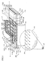
- Fig. 1 is a perspective view showing a construction of a semiconductor laser array apparatus LA1 according to a preferred embodiment of the invention
- Fig. 2 is a vertical sectional view taken on line A-A' in Fig. 1.
- the semiconductor laser array apparatus LA1 comprises a semiconductor laser array element 100 having a real refractive index guided self-aligned structure (RISA structure) and oscillating a laser beam of a wavelength corresponding to red, in which a plurality of single heterostrucutre members are fabricated on the same substrate, and an optical unit 200 condensing a plurality of laser beams into one spot.
- RISA structure real refractive index guided self-aligned structure
- the semiconductor laser array element 100 is configured so that two stripe-shaped laser oscillation units 300 and 310 are stacked on the same substrate in the vertical direction to the substrate, in which so-called single heterostructure members are laminated.
- a plurality of laser oscillation units 300 (310) are arranged side by side on the same layer and in the parallel direction to the substrate.
- the portion where a plurality of laser oscillation units 300 are arranged side by side in the parallel direction to the substrate is called a first laser array structure 301
- the portion above the first laser array structure 301 and where a plurality of laser oscillation units 301 are arranged side by side in the parallel direction to the substrate is called a second laser array structure 311.
- the semiconductor laser array element 100 comprises a structure in which an n-type GaAs substrate 101, an n-type GaAs buffer layer 102, an n-type AlGaInP first clad layer 103, a GaInP/AlGaInP quantum well structured first active layer 104, a p-type AlGaInP second clad layer 105, an n-type AlInP first current blocking layer 106, a p-type AlGaInP third clad layer 107, an n-type AlInP second current blocking layer 108, a p-type AlGaInP fourth clad layer 109, a GaInP/AlGaInP quantum well structured second active layer 110, an n-type AlGaInP fifth clad layer 111, an n-type GaAs contact layer 112 are laminated in this order, n-type electrodes 113A and 113B, and p-type electrodes 114A and 114B.
- the n-type electrodes 113A and 113B are sheet type electrodes provided on the top and bottom surface of the array structure.
- the n-type electrode 113A is a three-layered electrode made of AuGe/Ni/Au placed at the top surface
- the n-type electrode 113B is a three-layered electrode made of AuGe/Ni/Au placed at the bottom surface (at the substrate side).
- a pair of p-type electrodes 114A and 114B are strip shaped electrodes placed at right and left end portions of the array structure and on the surface 115A in two step portions 115 formed by removing both right and left ends of the array structure from the top surface to the vicinity of middle portion of the p-type AlGaInP third clad layer 107.
- the laser oscillation unit 300 consists of a portion between the n-type AlGaInP first clad layer 103 and the p-type AlGaInP third clad layer 107, while the laser oscillation unit 310 consists of a portion between the p-type AlGaInP third clad layer 107 and the n-type AlGaInP fifth clad layer 111.
- the optical unit 200 comprises a collimator lens 201 and a condenser lens 202.
- the collimator lens functions so that a plurality of laser beams 203 emitted from the both laser oscillation units 300 and 310, which are located at upper and lower portions in the semiconductor laser array element 100, becomes parallel to each other.
- the condenser lens 202 functions so that a plurality of parallel laser beams 204 from the collimator lens 201 are condensed into a spot SP.
- the collimator lens 202 it is preferable to employ a collimator lens which so that an optical path difference can be corrected in order not to cause a phase shift of the condensed laser beams.
- the following describes the first laser array structure 301 and the second laser array structure 311 in detail.
- the n-type AlInP first current blocking layer 106 consists of both ends portions 106A, a plurality of stripe portions 106B which have a discontiguous portion 106C in the middle thereof along the longitudinal direction and which are provided so as to be parallel to each other.
- the p-type AIGaInP third clad layer 107 is formed so as to be embedded into the discontiguous portions 106C and stripe-shaped grooves 106D formed between the end element 106A and stripe element 106B and between stripe elements 106B, and to cover all over the current blocking layer 106.
- the n-type AlInP second current blocking layer in the second laser array structure 311 placed above the first laser array structure 301 consists of both ends portions 108A and a plurality of stripe portions 108B which have a discontiguous portion 108C in the middle thereof along the longitudinal direction and provided so as to be parallel to each other in the same manner as the above n-type AlInP first current blocking layer 106.
- the p-type AlGaInP fourth clad layer 109 is formed so as to be embedded into the discontiguous portions 108C and stripe-shaped grooves 108D formed between the end element 108A and stripe element 108B and between stripe elements 108B, and to cover all over the current blocking layer 108.
- the laser oscillation units 300 and 310 including a region where laser beams are distributed consists of the portions including the active layers, the n-type clad layers and so on in the laser array structures.
- an electric power is applied to the portions of the clad layers embedded in the grooves 106D and 108D, and the distinguous portions 106C and 108C through portions above and below them. Then, these grooves 106D and 108D, and the distinguous portions 106C and 108C where the clad layers are embedded becomes a part of waveguides for laser beams.
- corresponding portions to the groove 106D and the distinguous portion 106C in the first laser array structure 301 are called a main waveguide 106E and a coupling waveguide 106F respectively
- the corresponding portions to the groove 108D and the distinguous portion 108C in the second laser array structure 311 are called a main waveguide 108E and a coupling waveguide 108F respectively.
- a distribution region 300A of the laser beam emitted from the laser oscillation unit 300 and a distribution region 310A of the laser beam emitted from the laser oscillation unit 310 at least contact or overlap with each other.
- Fig. 2 shows a state where the distribution regions overlap with each other. Note that, in this and the other embodiments of the invention, distribution regions of laser beams includes the region where a laser beam is leaked into the current blocking layer from the laser oscillation unit.
- the thickness of the p-type AlGaInP third clad layer 107 is specified.
- an energy of each laser oscillation unit is normally distributed so that an energy level is the highest in the active layer and gradually decreases with the distance from the active layer.
- the regions, whose energy are approximately 10% of that in the center of the distribution regions 300A and 310A of laser beams from the laser oscillation units 300 and 310 overlap with each other by means of the above-stated physical relationship.
- the laser oscillation units 300 and 310 are located close to each other the distribution region 300A of the laser beam from the laser oscillation unit 300 contacts or overlap with the distribution region 310A of the laser beam from the laser oscillation unit 310, whereby laser beams emitted from the laser oscillation units can be easily condensed by means of a common optical unit as stated above.
- the materials of the following parts are selected so that the forbidden band widths of the first and second current blocking layers are larger than those of portions of active layers under the portions of the third and fourth clad layers 107 and 109 embedded between elements of the first current blocking layer and between elements of the second current blocking layer, and refractive indexes of the first and second current blocking layers are smaller than the laser oscillation units located between the elements of the first current blocking layer and between patterns of the second current blocking layer.
- optical confinement effects can be obtained using a difference in real refractive indexes , while enabling an optical loss to reduce due to the absorption of laser beams into the current blocking layers.
- a film having a low reflection coefficient of the order of 1-15% is formed on the surface of the end facet 116 so that laser beams do not emit from the opposite end facet 117.
- Al 2 O 3 , SiO 2 , Si 3 N 4 , TiO 2 , and so on can be used as a material of the low-reflectance film, it is not limited to such materials .
- a film having a high reflection coefficient of the order of 70-98% is formed on the surface of the end facet 117.
- this high-reflectance film is formed by alternatively laminating a low refractive dielectric layer whose material is selected among Al 2 O 3 , SiO 2 , Si 3 N 4 , and so on, and a high refractive dielectric layer whose material is selected among TiO 2 , a-Si, hydrogenated a-Si, and so on , in two or more layers, it is not limited to such a construction.
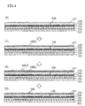
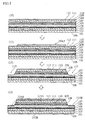
- Figs. 3 to 5 show the processes of manufacturing the semiconductor laser array element 100.
- an n-type GaAs substrate 101 is prepared.
- each of layers from an n-type GaAs buffer layer to a p-type AlGaInP second clad layer 105 is sequentially laminated on the n-type GaAs substrate 101 according to an MOCVD method or an MBE method.
- MOCVD method Metal Organic Chemical Vapor Deposition
- a material layer 106G to which patterning is performed to form an n-type InAlP first current blocking layer 106 is formed
- a mask layer MA1 is formed, whose pattern is an opposite pattern to the intended pattern of the n-type InAlP first current blocking layer 106.
- a liquid-phase etching is performed to unmasked portions, so that the pattern of the n-type InAlP first current blocking layer 106 is formed. Thereafter, the mask layer MA1 is removed.
- a p-type AlGaInP third clad layer is formed.
- a material layer 108G for an n-type InAlP second current blocking layer 108 is formed.
- a mask layer MA2 is formed, whose pattern is an opposite pattern to the intended pattern of the p-type InAlP second current blocking layer 108.
- a liquid-phase etching is performed to unmasked portions, so that the pattern of the n-type InAlP second current blocking layer 108 is formed into the material layer 108G. Thereafter, the mask layer MA2 is removed.
- each layer from a p-type AlGaInP fourth clad layer 109 to an n-type GaAs contact layer 112 is sequentially laminated.
- a mask layer MA3 is formed on the top surface of the n-type GaAs contact layer 112 other than both right and left end portions.
- a liquid-phase etching is performed to unmasked portions, so that both right and left end portions of each layer from the n-type GaAs contact layer 112 to the middle portion of the p-type AlGaInP third clad layer located below to form the step portion 115. Thereafter, the mask layer MA3 is removed.
- the array structure is formed.
- n-type electrodes 113A and 113B, and p-type electrodes 114A and 114B are formed at the predetermined positions respectively to complete the semiconductor laser array apparatus.
- laser beams do not interfere with each other so as to cancel each other out due to the phase shift at the spot where laser beams are condensed. Therefore, a high-power laser spot can be obtained in accordance with the number of installed laser oscillation units.
- phase locking is performed within each laser array structure and between different laser array structures.
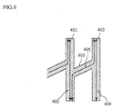
- Fig. 6 is a schematic diagram to explain the above-stated effect (i.e., a resonator shared effect) in detail.
- adjacent main waveguides 106E and 108E are coupled with each other by means of the coupling waveguides 106F and 108F. Therefore, it can be regarded as the state where so-called a resonator is shared.
- a resonator 402 formed with a main waveguide 401 in the longitudinal direction thereof and a resonator 404 formed with the other main waveguide 403 adjacent to the waveguide 401 in the longitudinal direction thereof are coupled with each other by means of a coupling waveguide 405. Therefore, it can be considered as a whole that a resonator 406 is formed so as to share a part of the resonators 402 and 404 and include a coupling waveguide 405, in addition to the resonators 402 and 404.
- phase locking can be performed between adjacent main waveguides in each of the first and second laser array structures 301 and 311. Naturally, phase locking is performed in a plurality of main waveguides in each of the first and second laser array structures 301 and 311 in the same manner.
- laser oscillation units 300 and 310 in the first laser array structure 301 and the second laser array structure 311 are located so that the distribution regions 300A and 310A of their laser beams contact or overlap with each other. Therefore, it can be considered that phase locking can be performed, because laser beams from upper and lower laser oscillation units 300 and 310 interfere with each other.
- phase locking can be performed for laser beams emitted from all laser oscillation units.
- laser oscillation units in each laser array structure are not necessarily located in the same position in the vertical direction to the substrate and parallel to each other.
- laser oscillation units 300 and 310 may be located to be displaced from each other in the vertical direction to the substrate.
- it may be configured so that distribution regions of laser beams from a laser oscillation unit 300 located at the right end of the first laser array structure 301 and a laser oscillation unit 301 located at the left end of the second laser array structure 311 only contact or overlaps with each other at one part. This is because phase locking can be performed between adjacent laser oscillation units in the same laser array structure (301 or 311) by means of the coupling waveguide as stated above.
- the laser oscillation units 300 and 301 in the first and second laser array structures 301 and 311 are located so as not to be parallel to each other but to cross each other.
- a semiconductor laser array apparatus in embodiment 2 is different from that of embodiment 1 in that it is formed by bonding two structures prepared in advance and including a first laser array structure 301 and a second laser array structure 311 respectively, whereas the semiconductor laser array apparatus in embodiment 1 is configured so that each layer is integrally formed according to the MOCVD or MBE method. The following describes difference points between them.
- Fig. 7 shows processes by which the apparatus according to embodiment 2 is manufactured.
- array structures 500 and 510 are manufactured according to the processes between Figs. 3 (1)-4 (6).
- the array structures 500 and 510 are superimposed so that their two p-type AlGaInP third clad layers are opposed to each other and laser oscillation units of them are aligned in the vertical direction to the substrate. Then heat treatment is conducted to adhere them according to hydrogen bond.
- the surfaces of the p-type AlGaInP third clad layers 107 in the two array structures 500 and 510 which are subjected to bonding should be cleaned to remove a natural oxidation film. Then, hydrophilic treatment is conducted by which hydroxyl groups are surfaced. It is desirable to superimpose array structures after the hydrophilic treatment, because they are integrated by hydrogen bond even in the room temperature, which leads to improve mechanical strength between bonded faces.
- the array structures 500 and 510 can be integrated with each other more firmly.
- a semiconductor laser array apparatus of embodiment 3 has the same construction as in the above semiconductor laser array apparatus LA1, except that shapes of the n-type AlInP first current blocking layer and the n-type AlInP second current blocking layer are different from those in LA1. The following describes difference points between them.
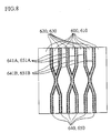
- Fig. 8 is a top plan view showing shapes of an n-type AlInP first current blocking layer 600 and an n-type AlInP second current blocking layer 610 in the semiconductor laser array apparatus according to embodiment 3.
- waveguides when looked down on from the top, are configured so as to bend like an X-shape at regions where the n-type AlInP first current blocking layer 600 and the n-type AlInP second current blocking layer 610 are not present, so that the adjacent waveguides merges with each other.
- the n-type AlInP first and second current blocking layers 600 and 610 comprise a plurality of regions respectively, and a p-type AlGaInP third and fourth clad layers 620 and 630 are embedded between adjacent regions.
- the waveguides 640 and 650 which are formed by these embedded portions with clad layers are shaped so as to merge with each other in the middle of their longitudinal directions like a letter X.
- the waveguides 640 and 650, which are formed between the adjacent regions of the n-type AlInP first current blocking layer 600 and between the adjacent regions of the n-type AlInP second current blocking layer 610 respectively, are called X junction waveguides 640 and 650.
- phase locking can be performed for each main waveguide, whereby laser beams do not interfere with each other so as to cancel each other out. Consequently, a high power laser spot according to the number of laser oscillation units can be obtained.
- a semiconductor laser array apparatus of embodiment 4 has the same construction as in the above semiconductor laser array apparatus LA1, except that shapes of the n-type AlInP first current blocking layer and the n-type AlInP second current blocking layer are different from those in LA1. The following describes difference points between them.
- Fig. 9 is a top plan view showing shapes of an n-type AlInP first current blocking layer 700 and an n-type AlInP second current blocking layer 710 in the semiconductor laser array apparatus according to the embodiment 4.
- n-type AlInP first and second current blocking layers 700 and 710 do not comprise a plurality of regions as in the above embodiment, but they are in contiguous sheet forms, where a plurality of short and long grooves 701 and 711 are formed so as to be parallel to each other in specific patterns. Then, p-type AlGaInP third and fourth clad layers are embedded in the grooves 701 and 711, respectively.
- the pattern in which the p-type AlGaInP third and fourth clad layers are embedded consists of stripes 702/703 and 712/713, which extend parallel to each other from either end portion to the vicinity of middle portion.
- each of these stripes 702/703 and 712/713 is positioned so as to have different phases.
- the distances between the stripes 702 and 703, and the stripes 712 and 713 are set so that their waveguide regions (regions where laser beam are leaked into the current blocking layers) contact or overlap with each other.
- the stripes 712, where the p-type AlGaInP fourth clad layer extended from one end of the apparatus is embedded into the current blocking layer, and the stripe 713 where the p-type AlGaInP fourth clad layer extended from the other end of the apparatus is embedded into the current blocking layer waveguide regions are located so that their distribution regions contact or overlap with each other between the stripes 712 and the stripes 713.
- the above construction allows laser beams to interfere with each other between waveguides 702 and 703, and 712 and 713, which are extended from different end facets. Therefore, phase locking can be performed for laser beams oscillated from each laser oscillation unit, so that laser beams do not interfere with each other so as to cancel each other out due to the phase shift at the spot where the laser beams are condensed. Consequently, a high-power laser spot can be obtained in accordance with the number of installed laser oscillation units.
- a semiconductor laser array apparatus of embodiment 5 has the same construction as in the above semiconductor laser array apparatus LA1, except that shapes of the n-type AlInP first current blocking layer and the n-type AlInP second current blocking layer, and the distance between adjacent laser oscillation units 300 and between those units 310 respectively are different from those in LA1. The following describes difference points between them.
- Fig. 10 is a sectional view of an semiconductor laser array apparatus according to the fifth embodiment, which corresponds to Fig. 2.
- distinguous portions are formed in the middle of the current blocking layers in the first and second laser array structure 301 and 311 respectively in the first embodiment, those portion are not formed but they have usual shapes in which extended stripe shapes are contiguously formed.
- stripes are narrower than those of the first embodiment, except in both ends regions of current blocking layers, whereby laterally adjacent laser oscillation units 300 and 310 respectively become closer to each other.
- the laterally adjacent laser oscillation units are positioned by specifying the width of the current blocking elements so that laterally adjacent distribution regions 300A (310A) of laser beams from laterally adjacent laser oscillation units 300 (310) contact or overlap with each other.
- the regions whose energy are approximately 10% of that in the center region of the distribution regions 300A and 310A of laser beams from the laser oscillation units 300 and 310 overlap with each other by means of the above-stated physical relationship in the same manner as in the above embodiment.
- phase locking can be performed for laser beams in the same laser array structure by allowing distribution regions of laser beams from horizontally adjacent laser oscillation units to contact or overlap with each other.
- interval between laterally adjacent laser oscillation units in each laser array structure may be either fixed or varied, which will be described in the following.
- the amount of emitted light tends to be smaller in the center portion than in the both ends portions, because it is hard to supply an electric power to the center portion.
- the heating value is larger in the center portion than in the both ends portions, because it is hard to dissipate heat in the center portion.
- a semiconductor laser array apparatus of embodiment 6 has the same construction as in the above semiconductor laser array apparatus LA1, except that an optical waveguide layer is interposed between the first laser array structure and the second laser array structure in order to condense their laser beams into their center portions. The following describes difference points between them.
- Fig. 11 is a sectional view of an semiconductor laser array element according to the sixth embodiment, which corresponds to Fig. 2.
- a p-type AlGaInP optical waveguide layer 800 is inserted in the vertically center portion of the p-type AlGaInP third clad layer 107.
- the p-type AlGaInP optical waveguide layer is interposed between the first laser array structure and the second laser array structure.
- composition and amount of impurities of the p-type AlGaInP optical waveguide layer 800 is specified so that its bandgap and refractive index are not smaller than those of the active layer and not larger than those of the p-type AlGaInP third clad layer 107.
- This p-type AlGaInP optical waveguide layer 800 enables laser beams oscillated from upper and lower laser oscillation units to condense into this layer (800). Therefore, as shown in Fig. 11, distribution regions of laser beams from upper and lower laser oscillation units can overlap in the optical waveguide layer, which is the same as in the first embodiment.
- phase locking can be performed by allowing laser beams from the corresponding upper and lower laser oscillation units to interfere with each other.
- the difference between the optical coupling method in the first and sixth embodiments are as follows.
- the semiconductor laser array apparatus of the first embodiment is adopted the optical coupling method (hereafter called "method A") by which the distance between the first and second laser array structures (i.e., the thickness of the clad layer between those layers) are specified so that distribution regions of laser beams from laser oscillation units contact or overlap with each other.
- method A optical coupling method
- this embodiment adopts the optical method (hereafter called “method B") which does not depend on the distance between the first and second laser array structures, but in which laser beams are condensed into the optical waveguide layer provided between the laser oscillation units.
- the optical waveguide layer is positioned so that the distribution regions of laser beams from upper and lower laser oscillation units contact or overlap with each other in this layer.
- both methods A and B are combined so that the upper and lower laser oscillation units become close to each other, while forming an optical waveguide layer of an optimum thickness interposed between those layers, laser beams from those laser oscillation units can be condensed into approximately one spot.
- a semiconductor laser array apparatus of the embodiment 7 is different from the above-stated semiconductor laser array apparatus LA1 in hat window mirror structures are formed at facets where both ends in the longitudinal direction of the laser oscillation unit in the semiconductor laser array apparatus face, and an insulating layer is formed at the top surface of each electrode positioned at regions where the window mirror structures are formed. The following describes difference points between them.
- Fig. 12 is a perspective view showing a construction of a semiconductor laser array apparatus according to the seventh embodiment.
- Zn is diffused at the regions where the both ends in the longitudinal direction of the laser oscillation units 300 and 310 face, so that a Zn diffusion portion 1000 is formed.
- This Zn diffusion portion 1000 forms the window mirror structure. This structure prevents laser beams from being absorbed at both ends of the laser oscillation units 300 and 310 in order not to generate heat there.
- SiO 2 insulating layers 1001, 1002, 1003, and 1004 are formed on the electrodes beneath which this Zn diffusion portion 1000 are formed. This structure further prevents an electric power from being applied at the end facets in order not to generate heat.
- the above-stated semiconductor laser array apparatus is configured so that the p-type AlGaInP second clad layer and the n-type AlInP first current blocking layer, and the p-type AlGaInP third clad layer and the n-type AlInP second current blocking layer directly contact with each other.
- a p-type InGaP etching stop layer can be formed between them. This p-type InGaP etching stop layer prevents oxidation of the surface of the current blocking layers. Therefore, current blocking layers with excellent crystalline structures can be formed.
- a hologram may be substituted for them. This makes a construction of the optical unit compact.
- red semiconductor laser is exemplified in this embodiment, it is naturally possible that this construction is applied to blue, green, infrared semiconductor lasers and the like.
- the two laser oscillation units are stacked in this embodiment, three or more units can be stacked. Thereby, much higher light output power can be realized.
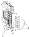
- Fig. 13 is a perspective view showing a construction of main elements of a multi-wavelength laser emitting apparatus according to the eighth embodiment.
- the multi-wavelength laser emitting apparatus 1101 comprises a light source unit 1102 emitting laser beams LB1 and LB2 whose wavelength are different from each other and consisting of semiconductor laser array apparatuses 1102A and 1102B, a collimate unit 1103 making laser beams LB1a and LB1b and LB2a and LB2b, which are emitted from the apparatuses 1102A and 1102B, parallel to each other, a reflecting unit 1104 reflecting laser beams LB1a, LB1b, LB2a, and LB2b so that all of them move parallel to each other in the same direction, a condenser lens 1105 condensing parallel laser beams LB1a, LB1b, LB2a, and LB2b into a predetermined condensing position on the optical axis, a condenser lens driving unit 1106 shifting the condenser lens 1105 along the optical axis, a control unit 1107 controlling the operation of
- the light source unit 1102 is configured so that the semiconductor laser array apparatuses 1102A and 1102B are arranged in parallel, which emits a plurality of laser beams LB1a and LB1b, and LB2a and LB2b moving in parallel with each other and whose wavelength are different from each other (i.e., wavelength is different between LB1 and LB2).
- the composition of the active layers in the semiconductor laser array apparatus 1102A and 1102B are different from each other, so that they emit laser beams with wavelengths corresponding to red and infrared regions, respectively.
- Each of a plurality of laser beams LB1a, LB1b (red), and LB2a and LB2b (infrared) from the same apparatus (1102A and 1102B) are emitted in a state where their phases and wavelengths are matched with each other (phase locking state). Thereby, a high-power laser beam can be obtained.
- the laser beams LB1a and LB1b, and LB2a and LB2b enter into hologram optical components 1103A and 1103B in the collimate unit 1103, respectively.
- the hologram optical components 1103A and 1103B are designed so as to make incident light, which diffuse after emitted from point light sources, parallel to each other, Thereby, laser beams passing through the hologram optical components 1103A and 1103B becomes parallel to each other.
- a collimate lens may be used as a means for making laser beams parallel to each other.
- the reflecting unit 1104 comprises a mirror 1104A reflecting parallel laser beams LB1 to the direction of the condenser lens 1105, and a half mirror 1104B reflecting parallel laser beams LB2 to the same direction.
- the half mirror 1104B is a well-known optical component for allowing a part of incident light to pass through, while reflecting the other part of light according to the incidence angle. In this case, this half mirror is fixed to a position so that main laser beams of LB1a, LB1b, LB2a, and LB2B form an angle of 45 degrees with respect to its incidence plane.
- laser beams LB1 reflected by the mirror 1104A pass through the half mirror 1104B, so that they moves parallel to the laser beams LB2 reflected by the half mirror 1104B to the direction of the condenser lens 1105.
- This enables laser beams LB1 and LB2 emitted from the different positions to move to the same direction, while most of laser beams are overlapped.
- the condenser lens 1105 functions so as to condense the incident laser beams LB1a, LB1b, LB2a, and LB2b into a predetermined condensing point on the optical axis.
- this condensing point on the optical axis varies in accordance with the difference in the wavelengths of incident light (longitudinal chromatic aberration). Therefore, their image formation points are different; a point SP1 (red) and a point SP2 (infrared).
- the apparatus of this embodiment is configured so that the position of the condenser lens 1105 can be adjusted along the optical direction according to the wavelength of a used laser.
- the condenser lens 1105 is supported to be movable along the optical axis and the condenser lens driving unit 1106 shifts this lens 1105 along the axis in accordance with the wavelength of a used laser, so that the condensing point of laser beams can be fixed regardless of their wavelength.
- the condenser lens 1105 is shifted by d (shown in Fig. 13) towards the reflecting unit 1104 along the optical axis in order to always condense laser beams into the spot SP1.
- the condenser lens driving unit 1106 includes a well-known fine adjustable linear actuator, such as a screw feed mechanism using ball screws.
- a screw feed mechanism using ball screws such as a screw feed mechanism using ball screws.
- the condensing position of laser beams can be adjusted by shifting at least one of those lenses along the optical axis.
- the control unit 1107 functions so as to control a travel of the lens driven by the condenser lens driving unit 1106, while controlling laser beams from the semiconductor laser array apparatuses 1102A and 1102B through a laser diode (LD) driving unit 1108.
- This unit switches on and off the semiconductor laser array apparatuses 1102A and 1102B so that a laser beam with a specified wavelength is outputted in accordance with the application.
- the control unit 1107 includes a program containing a travel data of the condenser lens varying from each semiconductor laser array apparatus, in advance. Therefore, the condensing position of laser beams can be fixed regardless of the wavelengths of laser beams, In case that a stepping motor is used to drive the condenser lens driving unit 1106, a travel can be easily controlled by the number of the driving pulses.
- Fig. 14 shows a modification of the multi-wavelength laser emitting apparatus according to the eighth embodiment.
- This apparatus is different from that in Fig. 13, in that the reflecting unit 1104 is removed and a hologram optical component 1109, which has a light condensing function, is provided in place of the condenser lens 1105. Since the hologram optical component 1109 has an advantage to be immune to optical distortion even when its diameter becomes large, there is no need to make laser beams LB1 and LB2 move in almost the same optical path by means of the half mirror 1104B as in Fig. 13. Instead, laser beams may enter to the hologram optical component 1109 with their interval maintained, which leads to downsizing for the apparatus.
- the hologram optical component 1109 is shifted along the optical axis according to the wavelength of emitted laser beams by a hologram driving unit 1110 in order to fix the condensing point of laser beams. Since the construction for adjusting is in the same manner as Fig. 13, the description will be omitted.
- Red laser made of AlGaInP (wavelength: 655 through 665 nm) :
- This laser may be applied for treatment for detached retinas by irradiating the light to the cornea.
- Green laser made of InGaN (wavelength 380nm; In 0.5 Ga 0.95 N) :
- This laser may be applied for treatment for myopia by irradiating the light to the cornea.
- Infrared laser made of InGaAs (wavelength 1060nm; In 0.2 Ga 0.9 As)
- this laser may be applied for treatment for detached retinas by irradiating the light to the cornea via an SHG element, which reduces a wavelength to the half, or the like.
Landscapes
- Physics & Mathematics (AREA)
- Health & Medical Sciences (AREA)
- Surgery (AREA)
- Life Sciences & Earth Sciences (AREA)
- Electromagnetism (AREA)
- Optics & Photonics (AREA)
- Engineering & Computer Science (AREA)
- Medical Informatics (AREA)
- Nuclear Medicine, Radiotherapy & Molecular Imaging (AREA)
- General Physics & Mathematics (AREA)
- Condensed Matter Physics & Semiconductors (AREA)
- Biomedical Technology (AREA)
- Heart & Thoracic Surgery (AREA)
- Otolaryngology (AREA)
- Molecular Biology (AREA)
- Animal Behavior & Ethology (AREA)
- General Health & Medical Sciences (AREA)
- Public Health (AREA)
- Veterinary Medicine (AREA)
- Semiconductor Lasers (AREA)
Abstract
Description
Claims (71)
- A semiconductor laser array apparatus, comprising:a first laser array structure which includes,a plurality of first laser oscillation units which are arranged side by side at an interval, anda first current blocking material which fills a space between each pair of adjacent first laser oscillation units; and,a second laser array structure which includes,a plurality of second laser oscillation units which are arranged side by side at an interval, anda second current blocking material which fills a space between each pair of adjacent second laser oscillation units,wherein, when the semiconductor laser array apparatus is activated, laser beams generated by the first laser array structure and the second laser array structure leak to the outside of the first and second laser array structures so as to form first and second distribution regions of the laser beams,and the first and second laser array structures are closely disposed so that the first and second distribution regions contact or overlap with each other.
- The semiconductor laser array apparatus of Claim 1,wherein a semiconductor layer is formed between the first and second laser array structures,a thickness of the semiconductor layer is adjusted so that the first and second distribution regions contact or overlap with each other.
- The semiconductor laser array apparatus of Claim 1, further comprising:an optical waveguide layer which is interposed between the first and second laser array structures, and introduces laser beams oscillated by each of the first and second laser oscillation units,wherein the first and second distribution regions contact or overlap with each other within the optical waveguide layer.
- The semiconductor laser array apparatus of Claim 1 and 2,wherein at least adjacent two laser oscillation units among the first laser oscillation units are optically coupled with each other,and at least adjacent two laser oscillation units among the second laser oscillation units are optically coupled with each other.
- The semiconductor laser array apparatus of Claim 3,wherein at least adjacent two laser oscillation units among the first laser oscillation units are optically coupled with each other,and at least adjacent two laser oscillation units among the second laser oscillation units are optically coupled with each other.
- The semiconductor laser array apparatus of Claim 4,wherein the first and second current blocking materials fill the spaces so as to form a plurality of first and second stripes, respectively,the optical coupling in the first laser oscillation units is conducted by means of coupling waveguides, each coupling waveguide is formed by removing a part of each of the first stripes in a stripe groove shape,and the optical coupling in the second laser oscillation units is conducted by means of coupling waveguides, each coupling waveguide is formed by removing a part of each of the second stripes in a stripe groove shape.
- The semiconductor laser array apparatus of Claim 5,wherein the first and second current blocking materials fill the spaces so as to form a plurality of first and second stripes, respectively,the optical coupling in the first laser oscillation units is conducted by means of coupling waveguides, each coupling waveguide is formed by removing a part of each of the first stripes in a stripe groove shape,and the optical coupling in the second laser oscillation units is conducted by means of coupling waveguides, each coupling waveguide is formed by removing a part of each of the second stripes in a stripe groove shape.
- The semiconductor laser array apparatus of Claim 4,wherein the optical coupling of the first laser oscillation units is conducted by allowing adjacent laser oscillation units to merge with each other,and the optical coupling of the second laser oscillation units is conducted by allowing adjacent laser oscillation units to merge with each other.
- The semiconductor laser array apparatus of Claim 5,wherein the optical coupling of the first laser oscillation units is conducted by allowing adjacent laser oscillation units to merge with each other,and the optical coupling of the second laser oscillation units is conducted by allowing adjacent laser oscillation units to merge with each other.
- The semiconductor laser array apparatus of Claim 4,wherein the first laser oscillation units has a plurality of first stripe-shaped patterns which are extended from one end facet of the apparatus and a plurality of second stripe-shaped patterns which are extended from the other end, the first and second stripe-shaped patterns are alternately arranged along the vertical direction to their longitudinal direction, andthe optical coupling of the first laser oscillation units is conducted between the first and second stripe-shaped patterns,the second laser oscillation units has a plurality of third stripe-shaped patterns which are extended from one end facet of the apparatus and a plurality of fourth stripe-shaped patterns which are extended from the other end, the third and fourth stripe-shaped patterns are alternately arranged along the vertical direction to their longitudinal direction, andthe optical coupling of the second laser oscillation units is conducted between the third and fourth stripe-shaped patterns.
- The semiconductor laser array apparatus of Claim 5,wherein the first laser oscillation units has a plurality of first stripe-shaped patterns which are extended from one end facet of the apparatus and a plurality of second stripe-shaped patterns which are extended from the other end, the first and second stripe-shaped patterns are alternately arranged along the vertical direction to their longitudinal direction, andthe optical coupling of the first laser oscillation units is conducted between the first and second stripe-shaped patterns,the second laser oscillation units has a plurality of third stripe-shaped patterns which are extended from one end facet of the apparatus and a plurality of fourth stripe-shaped patterns which are extended from the other end, the third and fourth stripe-shaped patterns are alternately arranged along the vertical direction to their longitudinal direction, and
the optical coupling of the second laser oscillation units is conducted between the third and fourth stripe-shaped patterns. - The semiconductor laser array apparatus of Claim 4,wherein the optical coupling of the first laser oscillation units is conducted by allowing the first distribution regions to contact or overlap with each other, andthe optical coupling of the second laser oscillation units is conducted by allowing the first distribution regions to contact or overlap with each other.
- The semiconductor laser array apparatus of Claim 5,wherein the optical coupling of the first laser oscillation units is conducted by allowing the first distribution regions to contact or overlap with each other, andthe optical coupling of the second laser oscillation units is conducted by allowing the first distribution regions to contact or overlap with each other.
- The semiconductor laser array apparatus of Claim 1 or 2, further comprising:a first electrode which has a first polarity, and which sandwiches the first laser array structure and the second laser array structure; anda second electrode which has a second polarity opposite to the first polarity, and which is formed on both end portions of a top surface of a conductive layer located between the first laser array structure and the second laser array structure.
- The semiconductor laser array apparatus of Claim 3, further comprising:a first electrode which has a first polarity, and which sandwiches the first laser array structure and the second laser array structure; anda second electrode which has a second polarity opposite to the first polarity, and which is formed on both end portions of a top surface of a conductive layer located between the first laser array structure and the second laser array structure.
- The semiconductor laser array apparatus of Claim 4, further comprising:a first electrode which has a first polarity, and which sandwiches the first laser array structure and the second laser array structure; anda second electrode which has a second polarity opposite to the first polarity, and which is formed on both end portions of a top surface of a conductive layer located between the first laser array structure and the second laser array structure.
- The semiconductor laser array apparatus of Claim 5, further comprising:a first electrode which has a first polarity, and which sandwiches the first laser array structure and the second laser array structure; anda second electrode which has a second polarity opposite to the first polarity, and which is formed on both end portions of a top surface of a conductive layer located between the first laser array structure and the second laser array structure.
- The semiconductor laser array apparatus of Claim 6, further comprising:a first electrode which has a first polarity, and which sandwiches the first laser array structure and the second laser array structure; anda second electrode which has a second polarity opposite to the first polarity, and which is formed on both end portions of a top surface of a conductive layer located between the first laser array structure and the second laser array structure.
- The semiconductor laser array apparatus of Claim 7, further comprising:a first electrode which has a first polarity, and which sandwiches the first laser array structure and the second laser array structure; anda second electrode which has a second polarity opposite to the first polarity, and which is formed on both end portions of a top surface of a conductive layer located between the first laser array structure and the second laser array structure.
- The semiconductor laser array apparatus of Claim 8, further comprising:a first electrode which has a first polarity, and which sandwiches the first laser array structure and the second laser array structure; anda second electrode which has a second polarity opposite to the first polarity, and which is formed on both end portions of a top surface of a conductive layer located between the first laser array structure and the second laser array structure.
- The semiconductor laser array apparatus of Claim 9, further comprising:a first electrode which has a first polarity, and which sandwiches the first laser array structure and the second laser array structure; anda second electrode which has a second polarity opposite to the first polarity, and which is formed on both end portions of a top surface of a conductive layer located between the first laser array structure and the second laser array structure.
- The semiconductor laser array apparatus of Claim 10, further comprising:a first electrode which has a first polarity, and which sandwiches the first laser array structure and the second laser array structure; anda second electrode which has a second polarity opposite to the first polarity, and which is formed on both end portions of a top surface of a conductive layer located between the first laser array structure and the second laser array structure.
- The semiconductor laser array apparatus of Claim 11, further comprising:a first electrode which has a first polarity, and which sandwiches the first laser array structure and the second laser array structure; anda second electrode which has a second polarity opposite to the first polarity, and which is formed on both end portions of a top surface of a conductive layer located between the first laser array structure and the second laser array structure.
- The semiconductor laser array apparatus of Claim 12, further comprising:a first electrode which has a first polarity, and which sandwiches the first laser array structure and the second laser array structure; anda second electrode which has a second polarity opposite to the first polarity, and which is formed on both end portions of a top surface of a conductive layer located between the first laser array structure and the second laser array structure.
- The semiconductor laser array apparatus of Claim 13, further comprising:a first electrode which has a first polarity, and which sandwiches the first laser array structure and the second laser array structure; anda second electrode which has a second polarity opposite to the first polarity, and which is formed on both end portions of a top surface of a conductive layer located between the first laser array structure and the second laser array structure.
- The semiconductor laser array apparatus of Claim 14, further comprising:
a window mirror structure which prevents heat generation and which is formed at end portions of the apparatus where the end portions of the first laser array structure and the second laser array structure face respectively. - The semiconductor laser array apparatus of Claim 15, further comprising:
a window mirror structure which prevents heat generation and which is formed at end portions of the apparatus where the end portions of the first laser array structure and the second laser array structure face respectively. - The semiconductor laser array apparatus of Claim 16, further comprising:
a window mirror structure which prevents heat generation and which is formed at end portions of the apparatus where the end portions of the first laser array structure and the second laser array structure face respectively. - The semiconductor laser array apparatus of Claim 17, further comprising:
a window mirror structure which prevents heat generation and which is formed at end portions of the apparatus where the end portions of the first laser array structure and the second laser array structure face respectively. - The semiconductor laser array apparatus of Claim 18, further comprising:
a window mirror structure which prevents heat generation and which is formed at end portions of the apparatus where the end portions of the first laser array structure and the second laser array structure face respectively. - The semiconductor laser array apparatus of Claim 19, further comprising:
a window mirror structure which prevents heat generation and which is formed at end portions of the apparatus where the end portions of the first laser array structure and the second laser array structure face respectively. - The semiconductor laser array apparatus of Claim 20, further comprising:
a window mirror structure which prevents heat generation and which is formed at end portions of the apparatus where the end portions of the first laser array structure and the second laser array structure face respectively. - The semiconductor laser array apparatus of Claim 21, further comprising:
a window mirror structure which prevents heat generation and which is formed at end portions of the apparatus where the end portions of the first laser array structure and the second laser array structure face respectively. - The semiconductor laser array apparatus of Claim 22, further comprising:
a window mirror structure which prevents heat generation and which is formed at end portions of the apparatus where the end portions of the first laser array structure and the second laser array structure face respectively. - The semiconductor laser array apparatus of Claim 23, further comprising:
a window mirror structure which prevents heat generation and which is formed at end portions of the apparatus where the end portions of the first laser array structure and the second laser array structure face respectively. - The semiconductor laser array apparatus of Claim 24, further comprising:
a window mirror structure which prevents heat generation and which is formed at end portions of the apparatus where the end portions of the first laser array structure and the second laser array structure face respectively. - The semiconductor laser array apparatus of Claim 25, further comprising:
a window mirror structure which prevents heat generation and which is formed at end portions of the apparatus where the end portions of the first laser array structure and the second laser array structure face respectively. - The semiconductor laser array apparatus of Claim 26, further comprising:
an insulating unit which is formed at portions where an electric power is applied to the surface of the window mirror structure. - The semiconductor laser array apparatus of Claim 27, further comprising:
an insulating unit which is formed at portions where an electric power is applied to the surface of the window. mirror structure. - The semiconductor laser array apparatus of Claim 28, further comprising:
an insulating unit which is formed at portions where an electric power is applied to the surface of the window mirror structure. - The semiconductor laser array apparatus of Claim 29, further comprising:
an insulating unit which is formed at portions where an electric power is applied to the surface of the window mirror structure. - The semiconductor laser array apparatus of Claim 30, further comprising:
an insulating unit which is formed at portions where an electric power is applied to the surface of the window mirror structure. - The semiconductor laser array apparatus of Claim 31, further comprising:
an insulating unit which is formed at portions where an electric power is applied to the surface of the window mirror structure. - The semiconductor laser array apparatus of Claim 32, further comprising:
an insulating unit which is formed at portions where an electric power is applied to the surface of the window mirror structure. - The semiconductor laser array apparatus of Claim 33, further comprising:
an insulating unit which is formed at portions where an electric power is applied to the surface of the window mirror structure. - The semiconductor laser array apparatus of Claim 34, further comprising:
an insulating unit which is formed at portions where an electric power is applied to the surface of the window mirror structure. - The semiconductor laser array apparatus of Claim 35, further comprising:
an insulating unit which is formed at portions where an electric power is applied to the surface of the window mirror structure. - The semiconductor laser array apparatus of Claim 36, further comprising:
an insulating unit which is formed at portions where an electric power is applied to the surface of the window mirror structure. - The semiconductor laser array apparatus of Claim 37, further comprising:
an insulating unit which is formed at portions where an electric power is applied to the surface of the window mirror structure. - The semiconductor laser array apparatus of Claim 1 or 2, wherein,forbidden bands of the first and second current blocking materials are wider than those of active layers in the first and second laser oscillation units respectively, andrefractive-indexes of the first and second current blocking materials are smaller than those of the first and second laser oscillation units.
- The semiconductor laser array apparatus of Claim 3, wherein,forbidden bands of the first and second current blocking materials are wider than those of active layers in the first and second laser oscillation units respectively, andrefractive-indexes of the first and second current blocking materials are smaller than those of the first and second laser oscillation units.
- The semiconductor laser array apparatus of Claim 4, wherein,forbidden bands of the first and second current blocking materials are wider than those of active layers in the first and second laser oscillation units respectively, andrefractive-indexes of the first and second current blocking materials are smaller than those of the first and second laser oscillation units.
- The semiconductor laser array apparatus of Claim 5, wherein,forbidden bands of the first and second current blocking materials are wider than those of active layers in the first and second laser oscillation units respectively, andrefractive-indexes of the first and second current blocking materials are smaller than those of the first and second laser oscillation units.
- A multi-wavelength laser emitting apparatus, comprising:a plurality of semiconductor laser array apparatuses which emit laser beams of different wavelength from each other; andan optical element which condenses the plurality of laser beams into a predetermined position;wherein at least one semiconductor laser array apparatus includes a plurality of laser array structures, each of which includes a plurality of laser oscillation units arranged side by side at an interval and a current blocking material filling the interval between each pair of adjacent laser oscillation units,and at least two adjacent laser array structures, among the plurality of laser array structures, are optically coupled with each other.
- The multi-wavelength laser emitting apparatus of Claim 54, further comprising:an adjusting means which adjusts a position where laser beams are condensed by shifting the optical element;a laser driving means which selects a laser array structure which emits laser beams of a designated wavelength and activates the selected laser array structure; anda control means which controls the adjusting means in accordance with the designated wavelength.
- The multi-wavelength laser emitting apparatus of Claim 54,wherein each of the plurality of semiconductor laser array apparatuses is a semiconductor laser array apparatus, comprising:a first laser array structure which includes,a plurality of first laser oscillation units which are arranged side by side at an interval, anda first current blocking material which fills a space between each pair of adjacent first laser oscillation units; and,a second laser array structure which includes,a plurality of second laser oscillation units which are arranged side by side at an interval, anda second current blocking material which fills a space between each pair of adjacent second laser oscillation units,wherein, when the semiconductor laser array apparatus is activated, laser beams generated by the first laser array structure and the second laser array structure leak to the outside of the first and second laser array structures so as to form first and second distribution regions of the laser beams,and the first and second laser array structures are closely disposed so that the first and second distribution regions contact or overlap with each other.
- The manufacturing method for the semiconductor laser array apparatus of Claim 2, comprising:a first step for forming the first laser array structure in which the plurality of first laser oscillation units are arranged side by side; anda second step for forming the second laser array structure in which the plurality of second laser oscillation units are arranged side by side so that a top surface of the second laser array structure faces a top surface of the first laser array structure,wherein, in the second step, the second laser array structure is formed on the first laser array structure according to an MOCVD method or an MBE method.
- The manufacturing method for the semiconductor laser array apparatus of Claim 3, comprising:a first step for forming the first laser array structure in which the plurality of first laser oscillation units are arranged side by side; anda second step for forming the second laser array structure in which the plurality of second laser oscillation units are arranged side by side so that a top surface of the second laser array structure faces a top surface of the first laser array structure,wherein, in the second step, after the optical waveguide layer is formed on the first laser array structure according to an MOCVD method or an MBE method, the second laser array structure is formed according to the same method.
- The manufacturing method for the semiconductor laser array apparatus of Claim 2, comprising:a first step for forming the first laser array structure in which the plurality of first laser oscillation units are arranged side by side;a second step for forming the second laser array structure in which the plurality of second laser oscillation units are arranged side by side; anda third step for attaching the first laser array structure to the second array structure.
- The manufacturing method for the semiconductor laser array apparatus of Claim 3, comprising:a first step for forming the first laser array structure in which the plurality of first laser oscillation units are arranged side by side;a second step for forming the second laser array structure in which the plurality of second laser oscillation units are arranged side by side; anda third step for attaching the first laser array structure to the second array structure,wherein, the third step follows a step for forming an optical waveguide layer on at least one surface of the first and second laser array structures.
- The manufacturing method of Claim 59, further comprising:a fourth step for conducting hydrophilic treatment to at least one surface of surfaces of the first and second laser array structures, prior to the third step,wherein heat treatment is conducted in the presence of hydrogen in the third step.
- The manufacturing method of Claim 60, further comprising:a fourth step for conducting hydrophilic treatment to at least one surface among surfaces of the optical waveguide layer, and the first and second laser array structures, prior to the third step,wherein heat treatment is conducted in the presence of hydrogen in the third step.
- A laser welding apparatus,
which uses laser beams emitted from a semiconductor laser array apparatus, comprising:a first laser array structure which includes,a plurality of first laser oscillation units which are arranged side by side at an interval, anda first current blocking material which fills a space between each pair of adjacent first laser oscillation units; and,a second laser array structure which includes,a plurality of second laser oscillation units which are arranged side by side at an interval, anda second current blocking material which fills a space between each pair of adjacent second laser oscillation units,wherein, when the semiconductor laser array apparatus is activated, laser beams generated by the first laser array structure and the second laser array structure leak to the outside of the first and second laser array structures so as to form first and second distribution regions of the laser beams,and the first and second laser array structures are closely disposed so that the first and second distribution regions contact or overlap with each other. - A two-dimensional matrix data manufacturing apparatus,
wherein two-dimensional matrix data is formed by irradiating a target with laser beams emitted from a semiconductor laser array apparatus, comprising:a first laser array structure which includes,a plurality of first laser oscillation units which are arranged side by side at an interval, anda first current blocking material which fills a space between each pair of adjacent first laser oscillation units; and,a second laser array structure which includes,a plurality of second laser oscillation units which are arranged side by side at an interval, anda second current blocking material which fills a space between each pair of adjacent second laser oscillation units,wherein, when the semiconductor laser array apparatus is activated, laser beams generated by the first laser array structure and the second laser array structure leak to the outside of the first and second laser array structures so as to form first and second distribution regions of the laser beams,and the first and second laser array structures are closely disposed so that the first and second distribution regions contact or overlap with each other. - A semiconductor laser scalpel apparatus, which is used for hemostasis and incising a living body by irradiating the living body with laser beams emitted a semiconductor laser array apparatus, comprising:a first laser array structure which includes,a plurality of first laser oscillation units which are arranged side by side at an interval, anda first current blocking material which fills a space between each pair of adjacent first laser oscillation units; and,a second laser array structure which includes,a plurality of second laser oscillation units which are arranged side by side at an interval, anda second current blocking material which fills a space between each pair of adjacent second laser oscillation units,wherein, when the semiconductor laser array apparatus is activated, laser beams generated by the first laser array structure and the second laser array structure leak to the outside of the first and second laser array structures so as to form first and second distribution regions of the laser beams,and the first and second laser array structures are closely disposed so that the first and second distribution regions contact or overlap with each other.
- A treatment apparatus for tumor,
wherein treatment is conducted against tumor by irradiating a living body after injection of photofrin with laser beams emitted from a semiconductor laser array apparatus, comprising:a first laser array structure which includes,a plurality of first laser oscillation units which are arranged side by side at an interval, anda first current blocking material which fills a space between each pair of adjacent first laser oscillation units; and,a second laser array structure which includes,a plurality of second laser oscillation units which are arranged side by side at an interval, anda second current blocking material which fills a space between each pair of adjacent second laser oscillation units,wherein, when the semiconductor laser array apparatus is activated, laser beams generated by the first laser array structure and the second laser array structure leak to the outside of the first and second laser array structures so as to form first and second distribution regions of the laser beams,and the first and second laser array structures are closely disposed so that the first and second distribution regions contact or overlap with each other. - A hair restoration treatment apparatus,
wherein hair restoration treatment is conducted by irradiating a head with laser beams emitted from a semiconductor laser array apparatus, comprising:a first laser array structure which includes,a plurality of first laser oscillation units which are arranged side by side at an interval, anda first current blocking material which fills a space between each pair of adjacent first laser oscillation units; and,a second laser array structure which includes,a plurality of second laser oscillation units which are arranged side by side at an interval, anda second current blocking material which fills a space between each pair of adjacent second laser oscillation units,wherein, when the semiconductor laser array apparatus is activated, laser beams generated by the first laser array structure and the second laser array structure leak to the outside of the first and second laser array structures so as to form first and second distribution regions of the laser beams,and the first and second laser array structures are closely disposed so that the first and second distribution regions contact or overlap with each other. - A treatment apparatus for detached retinas, wherein treatment is conducted against detached retinas by irradiating retinas with laser beams emitted from a semiconductor laser array apparatus, comprising:a first laser array structure which includes,a plurality of first laser oscillation units which are arranged side by side at an interval, anda first current blocking material which fills a space between each pair of adjacent first laser oscillation units; and,a second laser array structure which includes,a plurality of second laser oscillation units which are arranged side by side at an interval, anda second current blocking material which fills a space between each pair of adjacent second laser oscillation units,wherein, when the semiconductor laser array apparatus is activated, laser beams generated by the first laser array structure and the second laser array structure leak to the outside of the first and second laser array structures so as to form first and second distribution regions of the laser beams,and the first and second laser array structures are closely disposed so that the first and second distribution regions contact or overlap with each other.
- A treatment apparatus for myopia,
wherein treatment is conducted against myopia by irradiating corneas with laser beams emitted from a semiconductor laser array apparatus, comprising:a first laser array structure which includes,a plurality of first laser oscillation units which are arranged side by side at an interval, anda first current blocking material which fills a space between each pair of adjacent first laser oscillation units; and,a second laser array structure which includes,a plurality of second laser oscillation units which are arranged side by side at an interval, anda second current blocking material which fills a space between each pair of adjacent second laser oscillation units,wherein, when the semiconductor laser array apparatus is activated, laser beams generated by the first laser array structure and the second laser array structure leak to the outside of the first and second laser array structures so as to form first and second distribution regions of the laser beams,and the first and second laser array structures are closely disposed so that the first and second distribution regions contact or overlap with each other. - A punching and cutting apparatus,
wherein punching or cutting processing is performed by irradiating a target with laser beams emitted from a semiconductor laser array apparatus, comprising:a first laser array structure which includes,a plurality of first laser oscillation units which are arranged side by side at an interval, anda first current blocking material which fills a space between each pair of adjacent first laser oscillation units; and,a second laser array structure which includes,a plurality of second laser oscillation units which are arranged side by side at an interval, anda second current blocking material which fills a space between each pair of adjacent second laser oscillation units,wherein, when the semiconductor laser array apparatus is activated, laser beams generated by the first laser array structure and the second laser array structure leak to the outside of the first and second laser array structures so as to form first and second distribution regions of the laser beams,and the first and second laser array structures are closely disposed so that the first and second distribution regions contact or overlap with each other. - A surface treatment processing apparatus,
wherein surface treatment processing is performed by irradiating a target with laser beams emitted from a semiconductor laser array apparatus, comprising:a first laser array structure which includes,a plurality of first laser oscillation units which are arranged side by side at an interval, anda first current blocking material which fills a space between each pair of adjacent first laser oscillation units; and,a second laser array structure which includes,a plurality of second laser oscillation units which are arranged side by side at an interval, anda second current blocking material which fills a space between each pair of adjacent second laser oscillation units,wherein, when the semiconductor laser array apparatus is activated, laser beams generated by the first laser array structure and the second laser array structure leak to the outside of the first and second laser array structures so as to form first and second distribution regions of the laser beams,and the first and second laser array structures are closely disposed so that the first and second distribution regions contact or overlap with each other.
Applications Claiming Priority (4)
| Application Number | Priority Date | Filing Date | Title |
|---|---|---|---|
| JP2000099513 | 2000-03-31 | ||
| JP2000099514A JP2001284732A (en) | 2000-03-31 | 2000-03-31 | Multi-wavelength laser light emitting device, semiconductor laser array element used in the device, and method of manufacturing semiconductor laser array element |
| JP2000099513A JP2001284729A (en) | 2000-03-31 | 2000-03-31 | Semiconductor laser array device and method of manufacturing the same |
| JP2000099514 | 2000-03-31 |
Publications (2)
| Publication Number | Publication Date |
|---|---|
| EP1146617A2 true EP1146617A2 (en) | 2001-10-17 |
| EP1146617A3 EP1146617A3 (en) | 2003-04-23 |
Family
ID=26589253
Family Applications (1)
| Application Number | Title | Priority Date | Filing Date |
|---|---|---|---|
| EP01303078A Withdrawn EP1146617A3 (en) | 2000-03-31 | 2001-03-30 | High-powered semiconductor laser array apparatus |
Country Status (2)
| Country | Link |
|---|---|
| US (1) | US6556606B2 (en) |
| EP (1) | EP1146617A3 (en) |
Cited By (4)
| Publication number | Priority date | Publication date | Assignee | Title |
|---|---|---|---|---|
| WO2013116603A1 (en) * | 2012-02-02 | 2013-08-08 | Tria Beauty, Inc. | Dermatological treatment device with one or more multi-emitter laser diode |
| US9072533B2 (en) | 2011-03-30 | 2015-07-07 | Tria Beauty, Inc. | Dermatological treatment device with one or more multi-emitter laser diode |
| US9173708B2 (en) | 2011-03-30 | 2015-11-03 | Tria Beauty, Inc. | Dermatological treatment device with one or more laser diode bar |
| US11710942B2 (en) | 2017-12-13 | 2023-07-25 | Sony Corporation | Method of manufacturing light-emitting module, light-emitting module, and device |
Families Citing this family (7)
| Publication number | Priority date | Publication date | Assignee | Title |
|---|---|---|---|---|
| JP3950700B2 (en) * | 2002-02-12 | 2007-08-01 | 日本オプネクスト株式会社 | Manufacturing method of optical transmission module |
| JP2006093466A (en) * | 2004-09-24 | 2006-04-06 | Toshiba Corp | Multi-wavelength semiconductor laser device and multi-wavelength semiconductor laser device |
| US7652223B2 (en) * | 2005-06-13 | 2010-01-26 | Applied Materials, Inc. | Electron beam welding of sputtering target tiles |
| JP4756948B2 (en) | 2005-08-08 | 2011-08-24 | ベイバイオサイエンス株式会社 | Flow cytometer and flow cytometry method |
| EP3207602B1 (en) | 2014-10-15 | 2025-09-03 | Lumentum Operations LLC | Laser system and method of tuning the output power of the laser system |
| WO2021172350A1 (en) | 2020-02-26 | 2021-09-02 | ヌヴォトンテクノロジージャパン株式会社 | Light source module, processing machine, and processing method |
| CN115882340A (en) * | 2022-11-14 | 2023-03-31 | 深圳活力激光技术有限公司 | A semiconductor laser |
Family Cites Families (15)
| Publication number | Priority date | Publication date | Assignee | Title |
|---|---|---|---|---|
| JPS5552750A (en) * | 1978-10-12 | 1980-04-17 | Mochida Pharm Co Ltd | Laser knife* which can be detected* of tumor portion |
| US4541712A (en) * | 1981-12-21 | 1985-09-17 | Tre Semiconductor Equipment Corporation | Laser pattern generating system |
| DE3330293A1 (en) * | 1983-08-23 | 1985-03-14 | Alfred 7500 Karlsruhe Frank | Use of a laser light beam for reducing wrinkling of the skin or for improving or restoring hair growth |
| JPS62115795A (en) * | 1985-11-14 | 1987-05-27 | Matsushita Electric Ind Co Ltd | Semiconductor laser array device |
| US4722089A (en) * | 1985-12-16 | 1988-01-26 | Lytel, Incorporated | Phase locked diode laser array |
| US4730325A (en) * | 1986-03-17 | 1988-03-08 | The United States Of America As Represented By The Secretary Of The Air Force | Two-dimensional phase locked semiconductor laser array |
| JPS63142887A (en) * | 1986-12-05 | 1988-06-15 | Sharp Corp | Semiconductor light-emitting element |
| NL8800509A (en) * | 1988-02-29 | 1989-09-18 | Philips Nv | TWO-DIMENSIONAL LASER ARRAY. |
| CA2073802C (en) * | 1991-08-16 | 2003-04-01 | John Shimmick | Method and apparatus for combined cylindrical and spherical eye corrections |
| US5228103A (en) * | 1992-08-17 | 1993-07-13 | University Of Maryland | Monolithically integrated wavelength division multiplexing laser array |
| DE4234342C2 (en) * | 1992-10-12 | 1998-05-14 | Fraunhofer Ges Forschung | Process for material processing with laser radiation |
| US5487725A (en) * | 1994-05-12 | 1996-01-30 | Syntec, Inc. | Pneumatic vitrectomy for retinal attachment |
| FR2770695B1 (en) * | 1997-11-05 | 2000-03-24 | Thomson Csf | TAPE LASER AND MANUFACTURING METHOD |
| US6233045B1 (en) * | 1998-05-18 | 2001-05-15 | Light Works Llc | Self-mixing sensor apparatus and method |
| US6341118B1 (en) * | 1998-06-02 | 2002-01-22 | Science Applications International Corporation | Multiple channel scanning device using oversampling and image processing to increase throughput |
-
2001
- 2001-03-30 EP EP01303078A patent/EP1146617A3/en not_active Withdrawn
- 2001-04-02 US US09/824,470 patent/US6556606B2/en not_active Expired - Lifetime
Cited By (4)
| Publication number | Priority date | Publication date | Assignee | Title |
|---|---|---|---|---|
| US9072533B2 (en) | 2011-03-30 | 2015-07-07 | Tria Beauty, Inc. | Dermatological treatment device with one or more multi-emitter laser diode |
| US9173708B2 (en) | 2011-03-30 | 2015-11-03 | Tria Beauty, Inc. | Dermatological treatment device with one or more laser diode bar |
| WO2013116603A1 (en) * | 2012-02-02 | 2013-08-08 | Tria Beauty, Inc. | Dermatological treatment device with one or more multi-emitter laser diode |
| US11710942B2 (en) | 2017-12-13 | 2023-07-25 | Sony Corporation | Method of manufacturing light-emitting module, light-emitting module, and device |
Also Published As
| Publication number | Publication date |
|---|---|
| US20010026573A1 (en) | 2001-10-04 |
| EP1146617A3 (en) | 2003-04-23 |
| US6556606B2 (en) | 2003-04-29 |
Similar Documents
| Publication | Publication Date | Title |
|---|---|---|
| US6904068B2 (en) | Semiconductor laser device and multiple wavelength laser light emitting apparatus employing the semiconductor laser device | |
| JP2004304111A (en) | Multi-wavelength laser device | |
| CN109417276B (en) | Semiconductor laser device, semiconductor laser module, and laser light source system for welding | |
| EP3291387A1 (en) | Low power edge-emitting laser diode and laser diode module | |
| US6556606B2 (en) | High-powered semiconductor laser array apparatus in which the wavelength and phase of laser beams from semiconductor laser units above can be matched those of laser beams from semiconductor laser units below, manufacturing method of the semiconductor laser array apparatus and multi-wavelength laser emitting apparatus using the semiconductor laser array apparatuses | |
| JPWO2018168430A1 (en) | Semiconductor laser device, semiconductor laser module and laser light source system for welding | |
| JP7239920B2 (en) | Semiconductor optical amplifier, semiconductor optical amplifier, optical output device, and distance measuring device | |
| JP5187474B2 (en) | Semiconductor laser array and optical apparatus | |
| EP1258954A1 (en) | Semiconductor laser element, semiconductor laser module and production method therefor and optical fiber amplifier | |
| JP2001284732A (en) | Multi-wavelength laser light emitting device, semiconductor laser array element used in the device, and method of manufacturing semiconductor laser array element | |
| US6826224B2 (en) | High-power semiconductor laser array apparatus that outputs laser lights matched in wavelength and phase, manufacturing method therefor, and multi-wavelength laser emitting apparatus using such high-power semiconductor laser array apparatus | |
| US7300809B2 (en) | Optically pumped edge-emitting semiconductor laser | |
| US7095769B2 (en) | Semiconductor laser diode with higher-order mode absorption layers | |
| US7577174B2 (en) | Semiconductor laser device and semiconductor laser element array | |
| JP2001284729A (en) | Semiconductor laser array device and method of manufacturing the same | |
| JP2000138419A (en) | Semiconductor laser device and method of manufacturing the same | |
| JP4604639B2 (en) | Semiconductor laser device and manufacturing method thereof | |
| JP2025018195A (en) | Semiconductor laser element, and laser module, laser oscillator, and laser processing device equipped with the semiconductor laser element | |
| JP2006032407A (en) | Semiconductor laser device | |
| JP2827130B2 (en) | Semiconductor laser device and method of manufacturing the same | |
| US7505500B2 (en) | Laser diode and method of manufacturing the same | |
| JP4144257B2 (en) | Semiconductor laser and manufacturing method thereof | |
| JPS59175182A (en) | Semiconductor laser element | |
| JPH0567835A (en) | Manufacture of semiconductor laser | |
| JPH05283814A (en) | Semiconductor laser array element |
Legal Events
| Date | Code | Title | Description |
|---|---|---|---|
| PUAI | Public reference made under article 153(3) epc to a published international application that has entered the european phase |
Free format text: ORIGINAL CODE: 0009012 |
|
| AK | Designated contracting states |
Kind code of ref document: A2 Designated state(s): AT BE CH CY DE DK ES FI FR GB GR IE IT LI LU MC NL PT SE TR |
|
| AX | Request for extension of the european patent |
Free format text: AL;LT;LV;MK;RO;SI |
|
| 17P | Request for examination filed |
Effective date: 20020417 |
|
| PUAL | Search report despatched |
Free format text: ORIGINAL CODE: 0009013 |
|
| AK | Designated contracting states |
Designated state(s): AT BE CH CY DE DK ES FI FR GB GR IE IT LI LU MC NL PT SE TR |
|
| AX | Request for extension of the european patent |
Extension state: AL LT LV MK RO SI |
|
| 17Q | First examination report despatched |
Effective date: 20031117 |
|
| AKX | Designation fees paid |
Designated state(s): DE FR GB |
|
| STAA | Information on the status of an ep patent application or granted ep patent |
Free format text: STATUS: THE APPLICATION IS DEEMED TO BE WITHDRAWN |
|
| 18D | Application deemed to be withdrawn |
Effective date: 20040414 |