EP1146569A2 - Thin film forming method, thin film forming apparatus and solar cell - Google Patents
Thin film forming method, thin film forming apparatus and solar cell Download PDFInfo
- Publication number
- EP1146569A2 EP1146569A2 EP01108979A EP01108979A EP1146569A2 EP 1146569 A2 EP1146569 A2 EP 1146569A2 EP 01108979 A EP01108979 A EP 01108979A EP 01108979 A EP01108979 A EP 01108979A EP 1146569 A2 EP1146569 A2 EP 1146569A2
- Authority
- EP
- European Patent Office
- Prior art keywords
- thin film
- film forming
- frequency power
- inductive coupling
- coupling electrode
- Prior art date
- Legal status (The legal status is an assumption and is not a legal conclusion. Google has not performed a legal analysis and makes no representation as to the accuracy of the status listed.)
- Granted
Links
Images


Classifications
-
- H—ELECTRICITY
- H01—ELECTRIC ELEMENTS
- H01J—ELECTRIC DISCHARGE TUBES OR DISCHARGE LAMPS
- H01J37/00—Discharge tubes with provision for introducing objects or material to be exposed to the discharge, e.g. for the purpose of examination or processing thereof
- H01J37/32—Gas-filled discharge tubes
- H01J37/32431—Constructional details of the reactor
- H01J37/32532—Electrodes
-
- H—ELECTRICITY
- H01—ELECTRIC ELEMENTS
- H01J—ELECTRIC DISCHARGE TUBES OR DISCHARGE LAMPS
- H01J37/00—Discharge tubes with provision for introducing objects or material to be exposed to the discharge, e.g. for the purpose of examination or processing thereof
- H01J37/32—Gas-filled discharge tubes
- H01J37/32009—Arrangements for generation of plasma specially adapted for examination or treatment of objects, e.g. plasma sources
- H01J37/32082—Radio frequency generated discharge
- H01J37/321—Radio frequency generated discharge the radio frequency energy being inductively coupled to the plasma
-
- C—CHEMISTRY; METALLURGY
- C23—COATING METALLIC MATERIAL; COATING MATERIAL WITH METALLIC MATERIAL; CHEMICAL SURFACE TREATMENT; DIFFUSION TREATMENT OF METALLIC MATERIAL; COATING BY VACUUM EVAPORATION, BY SPUTTERING, BY ION IMPLANTATION OR BY CHEMICAL VAPOUR DEPOSITION, IN GENERAL; INHIBITING CORROSION OF METALLIC MATERIAL OR INCRUSTATION IN GENERAL
- C23C—COATING METALLIC MATERIAL; COATING MATERIAL WITH METALLIC MATERIAL; SURFACE TREATMENT OF METALLIC MATERIAL BY DIFFUSION INTO THE SURFACE, BY CHEMICAL CONVERSION OR SUBSTITUTION; COATING BY VACUUM EVAPORATION, BY SPUTTERING, BY ION IMPLANTATION OR BY CHEMICAL VAPOUR DEPOSITION, IN GENERAL
- C23C16/00—Chemical coating by decomposition of gaseous compounds, without leaving reaction products of surface material in the coating, i.e. chemical vapour deposition [CVD] processes
- C23C16/22—Chemical coating by decomposition of gaseous compounds, without leaving reaction products of surface material in the coating, i.e. chemical vapour deposition [CVD] processes characterised by the deposition of inorganic material, other than metallic material
- C23C16/24—Deposition of silicon only
-
- C—CHEMISTRY; METALLURGY
- C23—COATING METALLIC MATERIAL; COATING MATERIAL WITH METALLIC MATERIAL; CHEMICAL SURFACE TREATMENT; DIFFUSION TREATMENT OF METALLIC MATERIAL; COATING BY VACUUM EVAPORATION, BY SPUTTERING, BY ION IMPLANTATION OR BY CHEMICAL VAPOUR DEPOSITION, IN GENERAL; INHIBITING CORROSION OF METALLIC MATERIAL OR INCRUSTATION IN GENERAL
- C23C—COATING METALLIC MATERIAL; COATING MATERIAL WITH METALLIC MATERIAL; SURFACE TREATMENT OF METALLIC MATERIAL BY DIFFUSION INTO THE SURFACE, BY CHEMICAL CONVERSION OR SUBSTITUTION; COATING BY VACUUM EVAPORATION, BY SPUTTERING, BY ION IMPLANTATION OR BY CHEMICAL VAPOUR DEPOSITION, IN GENERAL
- C23C16/00—Chemical coating by decomposition of gaseous compounds, without leaving reaction products of surface material in the coating, i.e. chemical vapour deposition [CVD] processes
- C23C16/44—Chemical coating by decomposition of gaseous compounds, without leaving reaction products of surface material in the coating, i.e. chemical vapour deposition [CVD] processes characterised by the method of coating
- C23C16/50—Chemical coating by decomposition of gaseous compounds, without leaving reaction products of surface material in the coating, i.e. chemical vapour deposition [CVD] processes characterised by the method of coating using electric discharges
- C23C16/505—Chemical coating by decomposition of gaseous compounds, without leaving reaction products of surface material in the coating, i.e. chemical vapour deposition [CVD] processes characterised by the method of coating using electric discharges using radio frequency discharges
- C23C16/509—Chemical coating by decomposition of gaseous compounds, without leaving reaction products of surface material in the coating, i.e. chemical vapour deposition [CVD] processes characterised by the method of coating using electric discharges using radio frequency discharges using internal electrodes
-
- C—CHEMISTRY; METALLURGY
- C23—COATING METALLIC MATERIAL; COATING MATERIAL WITH METALLIC MATERIAL; CHEMICAL SURFACE TREATMENT; DIFFUSION TREATMENT OF METALLIC MATERIAL; COATING BY VACUUM EVAPORATION, BY SPUTTERING, BY ION IMPLANTATION OR BY CHEMICAL VAPOUR DEPOSITION, IN GENERAL; INHIBITING CORROSION OF METALLIC MATERIAL OR INCRUSTATION IN GENERAL
- C23C—COATING METALLIC MATERIAL; COATING MATERIAL WITH METALLIC MATERIAL; SURFACE TREATMENT OF METALLIC MATERIAL BY DIFFUSION INTO THE SURFACE, BY CHEMICAL CONVERSION OR SUBSTITUTION; COATING BY VACUUM EVAPORATION, BY SPUTTERING, BY ION IMPLANTATION OR BY CHEMICAL VAPOUR DEPOSITION, IN GENERAL
- C23C16/00—Chemical coating by decomposition of gaseous compounds, without leaving reaction products of surface material in the coating, i.e. chemical vapour deposition [CVD] processes
- C23C16/44—Chemical coating by decomposition of gaseous compounds, without leaving reaction products of surface material in the coating, i.e. chemical vapour deposition [CVD] processes characterised by the method of coating
- C23C16/50—Chemical coating by decomposition of gaseous compounds, without leaving reaction products of surface material in the coating, i.e. chemical vapour deposition [CVD] processes characterised by the method of coating using electric discharges
- C23C16/513—Chemical coating by decomposition of gaseous compounds, without leaving reaction products of surface material in the coating, i.e. chemical vapour deposition [CVD] processes characterised by the method of coating using electric discharges using plasma jets
-
- C—CHEMISTRY; METALLURGY
- C23—COATING METALLIC MATERIAL; COATING MATERIAL WITH METALLIC MATERIAL; CHEMICAL SURFACE TREATMENT; DIFFUSION TREATMENT OF METALLIC MATERIAL; COATING BY VACUUM EVAPORATION, BY SPUTTERING, BY ION IMPLANTATION OR BY CHEMICAL VAPOUR DEPOSITION, IN GENERAL; INHIBITING CORROSION OF METALLIC MATERIAL OR INCRUSTATION IN GENERAL
- C23C—COATING METALLIC MATERIAL; COATING MATERIAL WITH METALLIC MATERIAL; SURFACE TREATMENT OF METALLIC MATERIAL BY DIFFUSION INTO THE SURFACE, BY CHEMICAL CONVERSION OR SUBSTITUTION; COATING BY VACUUM EVAPORATION, BY SPUTTERING, BY ION IMPLANTATION OR BY CHEMICAL VAPOUR DEPOSITION, IN GENERAL
- C23C16/00—Chemical coating by decomposition of gaseous compounds, without leaving reaction products of surface material in the coating, i.e. chemical vapour deposition [CVD] processes
- C23C16/44—Chemical coating by decomposition of gaseous compounds, without leaving reaction products of surface material in the coating, i.e. chemical vapour deposition [CVD] processes characterised by the method of coating
- C23C16/50—Chemical coating by decomposition of gaseous compounds, without leaving reaction products of surface material in the coating, i.e. chemical vapour deposition [CVD] processes characterised by the method of coating using electric discharges
- C23C16/515—Chemical coating by decomposition of gaseous compounds, without leaving reaction products of surface material in the coating, i.e. chemical vapour deposition [CVD] processes characterised by the method of coating using electric discharges using pulsed discharges
-
- H—ELECTRICITY
- H10—SEMICONDUCTOR DEVICES; ELECTRIC SOLID-STATE DEVICES NOT OTHERWISE PROVIDED FOR
- H10F—INORGANIC SEMICONDUCTOR DEVICES SENSITIVE TO INFRARED RADIATION, LIGHT, ELECTROMAGNETIC RADIATION OF SHORTER WAVELENGTH OR CORPUSCULAR RADIATION
- H10F71/00—Manufacture or treatment of devices covered by this subclass
- H10F71/121—The active layers comprising only Group IV materials
-
- H—ELECTRICITY
- H10—SEMICONDUCTOR DEVICES; ELECTRIC SOLID-STATE DEVICES NOT OTHERWISE PROVIDED FOR
- H10P—GENERIC PROCESSES OR APPARATUS FOR THE MANUFACTURE OR TREATMENT OF DEVICES COVERED BY CLASS H10
- H10P14/00—Formation of materials, e.g. in the shape of layers or pillars
- H10P14/20—Formation of materials, e.g. in the shape of layers or pillars of semiconductor materials
- H10P14/24—Formation of materials, e.g. in the shape of layers or pillars of semiconductor materials using chemical vapour deposition [CVD]
-
- Y—GENERAL TAGGING OF NEW TECHNOLOGICAL DEVELOPMENTS; GENERAL TAGGING OF CROSS-SECTIONAL TECHNOLOGIES SPANNING OVER SEVERAL SECTIONS OF THE IPC; TECHNICAL SUBJECTS COVERED BY FORMER USPC CROSS-REFERENCE ART COLLECTIONS [XRACs] AND DIGESTS
- Y02—TECHNOLOGIES OR APPLICATIONS FOR MITIGATION OR ADAPTATION AGAINST CLIMATE CHANGE
- Y02E—REDUCTION OF GREENHOUSE GAS [GHG] EMISSIONS, RELATED TO ENERGY GENERATION, TRANSMISSION OR DISTRIBUTION
- Y02E10/00—Energy generation through renewable energy sources
- Y02E10/50—Photovoltaic [PV] energy
- Y02E10/547—Monocrystalline silicon PV cells
-
- Y—GENERAL TAGGING OF NEW TECHNOLOGICAL DEVELOPMENTS; GENERAL TAGGING OF CROSS-SECTIONAL TECHNOLOGIES SPANNING OVER SEVERAL SECTIONS OF THE IPC; TECHNICAL SUBJECTS COVERED BY FORMER USPC CROSS-REFERENCE ART COLLECTIONS [XRACs] AND DIGESTS
- Y02—TECHNOLOGIES OR APPLICATIONS FOR MITIGATION OR ADAPTATION AGAINST CLIMATE CHANGE
- Y02P—CLIMATE CHANGE MITIGATION TECHNOLOGIES IN THE PRODUCTION OR PROCESSING OF GOODS
- Y02P70/00—Climate change mitigation technologies in the production process for final industrial or consumer products
- Y02P70/50—Manufacturing or production processes characterised by the final manufactured product
Definitions
- the present invention relates to a thin film forming method, a thin film forming apparatus and a solar cell and, more particularly, to a thin film forming method and apparatus for forming a thin film of a-Si or the like having an excellent thickness uniformity over a large-sized substrate.
- a solar cell has been noted and expected as a clean energy source, but its cost reduction is indispensable for its spread. It has, therefore, been earnestly desired to provide a thin film forming apparatus which can uniformly form an a-Si film over a large-sized substrate at a high throughput.
- a parallel-plate (or capacitive coupling type) plasma-assisted CVD reactor For forming a thin film such as an a-Si film, there has been widely used a parallel-plate (or capacitive coupling type) plasma-assisted CVD reactor.
- this reactor has a disadvantage of low throughput because each run usually processes one substrate.
- the reactor to simultaneously process a plurality of substrates may become extremely large.
- a large-seized solar cell having desired characteristics can be hardly manufactured since the film thickness uniformity is seriously lowered with increasing the size of substrate.
- this method requires the precise arrangement of two plate electrodes with a prescribed distance all over the electrodes to generate uniform plasma, which is practically difficult as the substrate is larger.
- the standing wave tends to be generated on the electrode surfaces, which also lowers the uniformity of plasma density. This plasma distribution becomes more noticeable when the VHF frequency or higher frequency is employed.
- inductive coupling electrodes including those having the aforementioned electrodes
- the present inventors have found that as the size of inductive coupling electrodes such as the ladder-shaped or zigzag-folded electrodes is larger, the current flowing the electrode varies with the positions and the standing wave appears at unexpected positions. In short, it is difficult to create uniform plasma to cope with the large-sized substrate so far as electrode structures of the prior art are employed.
- the present inventors carried out fundamental investigations on the plasma homogenization using the inductive coupling electrodes and examined several electrode structure that positively utilizes the standing waves that caused the uniformity to deteriorate in the prior art inductive coupling electrodes .
- a rod-shaped and a U-shaped electrode were used, which have a power feeding portion and grounding portion at the respective ends.
- the distance between the grounding portion and the feeding portion was set to be natural number multiple of a half wavelength of the high-frequency wave to establish the standing wave at predetermined positions over the electrode so that the predictable plasma distribution may be utilized to form the thin film with uniform thickness on the substrate.
- the present inventors have further investigated the apparatus construction and the film forming conditions to eliminate the plasma density distribution caused by the attenuation of the high-frequency power and as a result found the following facts. That is, the state of the plasma is changed by amplitude-modulating the high-frequency power in a similarly way as the capacitive coupling PCVD although the plasma maintaining mechanism is absolutely different from each other. The distribution of the plasma density is also changed by the modulation condition and these changes have repeatability.
- the information is obtained for the first time by systematically investigating the film forming method using the inductive coupling electrodes, and the researches are further developed on the basis of the discoveries to clarify the relations between the feeding method and the modulation method, and the thin film distribution.
- the present invention has been accomplished.
- An object of the present invention is to provide a thin film forming method and apparatus which make it possible to form a thin film having an excellent thickness uniformity over a large-sized substrate.
- Another object of the invention is to provide a thin film forming method and apparatus which make it possible to form a thin film having excellent characteristics and thickness uniformity at high throughput.
- Still another object of the invention is to fabricate a solar cell by using the aforementioned thin film forming method or apparatus and to provide a high-quality, low-cost solar cell.
- a thin film forming method comprising: the step of arranging an inductive coupling electrode having a power feeding portion and a grounding portion in a film forming chamber; and the step of feeding an amplitude-modulated high-frequency power to said feeding portion to generate a plasma to form a thin film over a substrate arranged to face the inductive coupling electrode.
- the uniform plasma density distribution can be achieved by selecting the proper modulation method. For example, even under the condition for forming a high quality film at a high rate, the plasma density can be made uniform to form the thin film with uniform thickness.
- the "amplitude modulation" has a meaning including the pulse modulation.
- the amplitude modulation that cuts off the high-frequency power periodically is used.
- the ratio of a period for feeding the high-frequency power is preferably varied.
- the modulation frequency of the amplitude modulation is preferably varied.
- the inductive coupling electrode of the invention is properly exemplified by either an electrode having a shape folded at the center or a rod-shaped electrode. It is preferred that the frequency of the high-frequency power is changed to establish standing waves between the feeding portion and the folded portion of the inductive coupling electrode or between the feeding portion and the grounding portion.
- the inductive coupling electrode having the center-folded shape is disposed in plurality in parallel in a common plane, and that the high-frequency powers in anti-phase are fed to the adjacent feeding portions.
- the film thickness distribution not only in the widthwise direction of the substrate but also in the longitudinal direction of the electrodes can be improved. This makes it possible to form a thin film with uniform thickness over a larger substrate.
- the plasma density can be further homogenized for the various film forming conditions by selecting the proper modulation conditions and by feeding anti-phase high-frequency powers to the adjacent electrodes.
- a thin film forming apparatus comprising: a film forming chamber in which an inductive coupling electrode having a feeding portion and a grounding portion at its two ends is arranged; a high-frequency power source for feeding a high-frequency power to the feeding portion; and a waveform generator for amplitude-modulating the high-frequency power outputted from the high-frequency power source, whereby the amplitude-modulated high-frequency power is fed to the inductive coupling electrode to generate a plasma so that a thin film may be formed on a substrate arranged to face the inductive coupling electrode.
- the apparatus construction in which a plurality of electrodes having a rod shape or a center-folded shape are arranged in a common plane is preferably used.
- the distance between the feeding portion and the grounding portion of the rod-shaped electrode or between the feeding portion and the turning portion of the center-folded shape electrode is set to be natural number multiple of a half wavelength of the high-frequency wave. It is possible to generate and maintain the plasma more stably thereby and to reproducibly form a thin film having uniform thickness.
- the inductive coupling electrode having the center-folded shape is arranged in plurality in parallel in a common plane, and there is further comprised means for controlling the phase of the high-frequency power to be fed to the feeding portions such that the high-frequency waves in anti-phase are fed to the adjacent feeding portions of the plurality of inductive coupling electrodes.
- the inductive coupling electrode planes are arranged in a plurality of layers, and substrates are arranged on the two sides of each electrode layer so that thin films may be simultaneously formed on the plurality of substrates. That is, by using the inductive coupling electrodes, the so-called "multi-zone film forming method" can be adopted, without inviting the enlargement of the apparatus unlike the case of the capacitive coupling electrode. Thus, a film forming apparatus which forms thin films simultaneously on a number of substrates can be constructed. As a result, the throughput can be drastically improved to lower the cost of e.g. the solar cell.
- a solar cell of the present invention is manufactured to include at least one of its thin films formed by the aforementioned thin film forming method or thin film forming apparatus of the present invention.
- uniform thin films with various qualities can be prepared since the conditions for forming a high quality film at a high rate can be selected.
- the cost for manufacturing the solar cell can be lowered while keeping the high quality.
- the multi-zone film forming method moreover, the higher throughput can be achieved, which contributes to further cost reduction of solar cells.
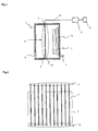
- a film forming chamber 1 which is provided with a gas inlet 5 and an exhaust port 6, as shown in Fig. 1, there is arranged an inductive coupling electrode 2, one end of which is a grounding portion 10 connected to the wall of the film forming chamber in the earth potential, and the other end of which is a feeding portion 9 connected to a high-frequency power source 3 through a coaxial cable 14.
- a waveform generator 4 To this high-frequency power source 3, there is connected a waveform generator 4 so that the high-frequency power to be outputted from the power source can be desirably amplitude-modulated.
- numeral 7 designates a substrate
- numeral 8 designates a substrate heating heater.
- the inductive coupling electrode 2 is provided at its two end portions with the feeding portion 9 and the grounding portion 10 as mentioned.
- the distance L between the feeding portion 9 and the grounding portion 10 is preferred to be n/2 times (n: a natural number) of an excitation wavelength ⁇ of the high-frequency power.
- the oscillatory frequency of the high-frequency power source may be made variable so that the frequency may be changed to satisfy the aforementioned equation for a predetermined value of the distance L.
- the apparatus of Fig. 1 is constructed to arrange the single electrode.
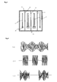
- a plurality of electrodes may be arrayed to correspond to the substrate width, as shown in Fig. 2, and may be individually fed with the high-frequency power.
- the thin film forming apparatus of the invention is preferably given a structure of a multi-zone film forming type, in which the electrodes arrayed in the substrate width in a common plane and then the electrode planes are arranged in a plurality of layers spaced at a predetermined interval, as shown in Fig. 3, so that the substrates may be arranged on the two sides of each electrode layer.
- the thin films can be simultaneously formed on a multiplicity of substrates (or six in the shown embodiment), to raise the throughput drastically.
- the distance between the electrodes and the substrates can be made as small as about 30 to 60 mm to form the films simultaneously over the numerous substrates in the small space. It is, therefore, possible to realize a thin film forming apparatus which has an excellent throughput ratio to the installation area of the apparatus.
- Figs. 1 to 3 there have been used the rod-shaped electrodes, to which the inductive coupling electrodes of the invention should not be limited but can also be properly exemplified by electrodes folded at centers, as shown in Fig. 8.
- the electrodes are provided at their two end portions with the feeding portions 9 and the grounding portion 10.
- the center-folded shape is exemplified by the shape of letter "U” or the rectangularly folded shape, which should not be limited to one folded rod but may be exemplified by a structure in which two straight electrodes are jointed and fixed with a metal plate or the like.
- the distance between the feeding portion 9 and the grounding portion 10, and turning portion 15 are preferred to be n/2 times (n: a natural number) as long as the excitation wavelength ⁇ of the high-frequency power.
- n a natural number
- the feeding portion and the grounding portion need not always be disposed in the film forming chamber, as in the case of the rod-shaped electrodes.
- the turning portion is exemplified by semicircular portions having a curvature in the case of the U-shape and by shorter straight portion between the two longer straight portions in the case of the rectangularly folded shape.
- the high-frequency power source is properly exemplified by a high-frequency power source of a VHF band of 20 to 600 MHz, and the invention should not be limited thereto but can use microwaves.
- a conversion connector with the coaxial cable may be connected with the waveguide, and the coaxial cable may be connected with the feeding portion.
- the waveform generator 4 is provided for amplitude-modulating the high-frequency power. That is, the high-frequency power, as outputted from the high-frequency power source 3, is amplitude-modulated by the waveform generator 4 so that the high-frequency power having the waveforms, as illustrated in Fig. 4, is fed to the feeding portion of the inductive coupling electrodes.
- the signal waves to modulate the high-frequency power may have any waveforms such as s sin wave (Fig. 4(a)), s rectangular wave, s triangular wave, a wave having waveform to cut off the output completely for a predetermined period (Fig. 4(b)), and a wave superposing the foregoing waves (Fig. 4(c)).
- the film forming chamber 1 is evacuated at first to a high vacuum, and the substrate 7 is then heated to a predetermined temperature by the heater.
- a reaction gas for the deposition is introduced at a predetermined flow rate into the film forming chamber, and the inside of the film forming chamber is set to a predetermined pressure by the main valve which is disposed in the exhaust port.
- the high-frequency power source 3 and the waveform generator 4 are turned ON to feed the inductive coupling electrode 2 with the high-frequency power which has been amplitude-modulated with the predetermined signal wave.
- a plasma is generated around the electrodes so that the reactive gas can be decomposed and activated to form a thin film having an excellently uniform thickness over the substrate 7.
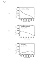
- the present inventors performed experiments to form the a-Si thin film over the substrate, by introducing a S i H 4 gas into the film forming chamber of Fig. 5 and by amplitude-modulating the high-frequency power under various modulation conditions to generate the plasmas along the electrodes.
- the electrodes there were used in the experiments the rod-shaped electrodes having an outer diameter of 10 mm and a length of 1.6 m, and these eight electrodes were arranged to have a center distance of 32.5 mm.
- the electrode-substrate distance was 50 mm.
- a substrate (having a length of 500 mm) 12 was arranged in the film forming chamber 1 and was heated to 200 °C, and the S i H 4 gas is introduced at 300 sccm to set the pressure at 5 Pa.
- the high-frequency powers, as modulated under the various conditions, were fed to the electrodes to generate the plasmas thereby to form the a-Si thin films over the substrates.
- the high frequency was 80 MHz
- the fed electric power was 31 W (for each electrode); and the high-frequency powers at the feeding portions of the individual electrodes were in phase.
- Fig. 6(a) is a graph plotting the film thickness distribution, as taken in the electrode direction, when the high-frequency power was fed (for continuous discharge) without any modulation to form the thin films.
- the electrode center point corresponds to the position of 250 mm of the graph.
- Figs. 6 (b) and 6(c) plot the film thickness distributions when the a-Si thin films were formed by changing the percentage modulation and the modulation frequency, respectively.
- Figs. 7 (a) and 7 (b) plot the film thickness distributions when the a-Si thin films were formed by changing the duty ratios (or pulse modulations).
- Fig. 7(c) plots the film thickness distribution at the time when the a-Si film was formed by adjusting the modulation conditions so as to homogenize the plasma density along the electrodes and by cutting off the feed of the high-frequency power periodically, as illustrated in Fig. 4(c).
- the a-Si film having an extremely excellent uniformity can be formed by superposing the pulse modulation over the amplitude modulation of 1 kHz.
- the thin film forming apparatus of the prior art can form a film having a highly uniform thickness under certain conditions but is troubled by a problem that the uniform thickness cannot be achieved under the film forming conditions for a high quality film, for example.
- the plasma density distribution change can be corrected by optimizing the amplitude modulations, to form the thin film which is excellent in the film thickness uniformity.
- the plasma density on the feeding portion side is higher than on the grounding portion side.
- the plasma density can be made uniform along the electrodes by raising the percentage of the amplitude modulation, by raising the modulation frequency or by lowering the duty ratio in the pulse modulation case, or by combining these methods. If the pressure is raised from the viewpoint of the film quality or the film forming rate, on the other hand, the plasma density on the feeding side becomes lower. Therefore, the reverse operations may be made to flatten the plasma density.
- a thin film with uniform thickness can be formed under any film forming condition. According to the invention, therefore, it is possible to form a thin film with a high quality and a uniform thickness at a high rate.
- the thin film may be formed by feeding the electrodes with the high-frequency power which has been amplitude-modulated by the modulation condition optimized in advance for the film forming condition, but the modulation condition may be changed during the film formation, observing the state of the plasma.
- the uniform thickness film can also be prepared.
- the modulation conditions may be changed while the thin film is being formed, so that the film thickness may be finally uniform all over the substrate. It is preferable to change the modulation frequency of the amplitude modulation or the duty ratio of the pulses. By this film forming method, it is also possible to form a film having a different quality in the thickness direction, for example.
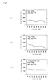
- a plurality of U-shaped inductive coupling electrodes 2 are arranged in the film forming chamber 1 having the gas inlet 5 and the exhaust port 6. Each electrode is grounded by connecting its one end grounding portion 10 with the wall of the film forming chamber 1, and the feeding portion 9 at its other end is connected with the high-frequency power source 3 through the coaxial cable 14.
- a phase shifter 13 is arranged between the feeding portion 9 and the high-frequency power source 3. With this high-frequency power source 3, moreover, there is connected the waveform generator 4 so that a desired amplitude modulation can be applied to the high-frequency power to be outputted from the power source 3.
- the inductive coupling electrode 2 is exemplified by the U-shaped electrode which is folded back at its center, and is provided at its two end portions with the feeding portion 9 and the grounding portion 10.
- the distance L between the feeding portion 9 and the grounding portion 10, and the turning portion 15 is preferred to be n/2 times (n: a natural number) as long as the excitation wavelength ⁇ of the high-frequency power.
- the phase shifter 13 for controlling the phase of high-frequency power is arranged as the means for feeding the high-frequency waves in anti-phase to the feeding portions of the adjacent ones of the plurality of inductive coupling electrodes.
- the number of electrodes is large as in the case of Fig. 3.
- the number of phase shifters becomes the larger for the larger number of electrodes, and all of the phase shifters have to be individually adjusted to control the phases of the adjacent electrodes.
- only one phase shifter 13 is sufficient irrespective of the number of electrodes, so that the system can be simplified. Therefore, the phase adjustment may be made for the single phase shifter.
- the phases of the feeding portions of the adjacent electrodes can be inverted.
- the distance between the feeding portion and the turning portion are elongated alternately of the plurality of electrodes to a half wavelength of the high-frequencywave, and the feeding portions are disposed outside of the film forming chamber.
- a coaxial cable equivalent to the half wavelength may be added to each feeding portion.
- the film forming chamber 1 is evacuated, and the substrate 7 is then heated by the (not-shown) heater to a predetermined temperature.
- the reactive gas for the deposition is introduced at a predetermined flow rate into the film forming chamber, and the inside of film forming chamber is set to a predetermined pressure by the main valve which is disposed in the exhaust port 6.
- the high-frequency power source 3 and the waveform generator 4 are turned ON, and the high-frequency power are amplitude-modulated with a predetermined signal wave.
- the phases of the feeding portions of the adjacent electrodes are adjusted to take a phase shift of 180 degrees by the phase shifters.
- the plasmas with uniform density are generated around the electrodes to decompose and activate the reactive gas so that a thin film having an excellently uniform thickness can be formed over the substrate 7.
- Figs. 10 (a) to 10 (e) are graphs plotting the film thickness distributions which were measured in the longitudinal direction of the electrodes when the a-Si films were formed under the following film forming conditions.
- Figs. 10(a) to 10(c) plot the film thickness distributions which were obtained when the pulses were modulated with different frequencies and when the high-frequency waves in anti-phase were fed to the adjacent electrodes.
- Figs. 10(d) and 10(e) plot the film thickness distributions which were obtained when the in-phase high-frequency power was fed to the individual electrodes and with the pulse modulation (Fig. 10(d)) of 300 Hz and in the continuous discharge (Fig. 10(e)) with no modulation.
- the film thickness distribution was such that the film thickness was large on the feeding portion side, reduced toward the turning portion, then increased to the maximum, and reduced again.
- This film thickness distribution is observed where the in-phase high-frequency wave is fed to form a film on a large-sized substrate (1m) as large as the electrode length (1.35 m).
- the high-frequency waves in anti-phase are fed to the adjacent electrodes, on the contrary, a generally flattened distribution can be obtained, as compared with the case of the in-phase.
- the relative film thickness ratio is given a tendency to change between the feeding portion side and the end side (folded portion side) of the electrodes by changing the frequency of the pulse modulation.
- the plasma density can be made uniform under the various film forming conditions so that a thin film having an excellently uniform thickness can be formed even over a large-sized substrate of 1 m or more.
- the thin film forming apparatus and method of the invention have been described mainly on the case in which the invention is applied to the a-Si film. However, it is quite natural that the invention can be applied not only to the a-Si film but also the various thin films by selecting the reactive gases.
- the films can be simultaneously formed on a number of substrates without inviting the size enlargement of the apparatus. As a result, the films can be formed with high throughput to achieve the highest target, i.e., to lower the cost for spreading the use of solar cells.
- the solar cells may be constructed to have the p-i-n structure, the p-n structure or the tandem structure having the foregoing structures laminated.
- the thin film forming method and the thin film forming apparatus of the present invention can be applied to those p-layer, i-layer and n-layer.
- a thin film having an excellent thickness uniformity can be formed on a large-sized substrate by the thin film forming method and the thin film forming apparatus of the invention. Moreover, it is possible to provide a thin film forming apparatus which has a high throughput ratio to the apparatus installation area.
Landscapes
- Chemical & Material Sciences (AREA)
- Engineering & Computer Science (AREA)
- Physics & Mathematics (AREA)
- Plasma & Fusion (AREA)
- Chemical Kinetics & Catalysis (AREA)
- General Chemical & Material Sciences (AREA)
- Materials Engineering (AREA)
- Mechanical Engineering (AREA)
- Metallurgy (AREA)
- Organic Chemistry (AREA)
- Analytical Chemistry (AREA)
- Inorganic Chemistry (AREA)
- Photovoltaic Devices (AREA)
- Chemical Vapour Deposition (AREA)
Abstract
Description
81 MHz, 25 W (for each)
SiH4, 300 sccm
5 Pa
Claims (18)
- A thin film forming method comprising:the step of arranging an inductive coupling electrode having a power feeding portion and a grounding portion at its two ends in a film forming chamber; andthe step of feeding an amplitude-modulated high-frequency power to said feeding portion to generate a plasma to form a thin film on a substrate arranged to face said inductive coupling electrode.
- A thin film forming method according to Claim 1,
wherein said inductive coupling electrode has a rod shape. - A thin film forming method according to Claim 2, further comprising:
the step of adjusting the frequency of the high-frequency power to establish a standing wave between the feeding portion and the grounding portion of said inductive coupling electrode. - A thin film forming method according to Claim 1,
wherein said inductive coupling electrode has a shape in which it is folded back at its center. - A thin film forming method according to Claim 4,wherein said inductive coupling electrode is disposed in plurality in parallel in a common plane, andwherein the phase of the high-frequency powers is made in anti-phase between the adjacent feeding portions.
- A thin film forming method according to Claim 4 or 5, further comprising:
the step of adjusting the frequency of the high-frequency power to establish a standing wave between the feeding portions and the turning portion of said inductive coupling electrode. - A thin film forming method according to one of Claims 1 to 6,
wherein said amplitude modulation cuts off the feed of the high-frequency power periodically. - A thin film forming method according to one of Claims 1 to 7,
wherein the modulation frequency of said amplitude modulation is varied while the thin film is being formed. - A thin film forming method according to Claim 7,
wherein the ratio of a period for feeding the high-frequency power is varied while the thin film is being formed. - A thin film forming apparatus comprising:a film forming chamber in which an inductive coupling electrode having a power feeding portion and a grounding portion at its two ends is arranged;a high-frequency power source for feeding a high-frequency power to said feeding portion; anda waveform generator for amplitude-modulating the high-frequency power outputted from said high-frequency power source,whereby the amplitude-modulated high-frequency power is fed to said inductive coupling electrode to generate a plasma so that a thin film may be formed on a substrate arranged to face said inductive coupling electrode.
- A thin film forming apparatus according to Claim 10,
wherein said inductive coupling electrode has a rod shape. - A thin film forming apparatus according to Claim 11,
wherein said inductive coupling electrode is arranged in plurality in a common plane. - A thin film forming apparatus according to Claim 11,
wherein the distance between said feeding portion and said grounding portion is natural number multiple of a half wavelength of said high-frequency power. - A thin film forming apparatus according to Claim 10,
wherein said inductive coupling electrode has a shape in which it is folded back at its center. - A thin film forming apparatus according to Claim 14,wherein said inductive coupling electrode is arranged in plurality in parallel in a common plane,further comprising means for controlling the phase of the high-frequency power such that the phase of the high-frequency powers is made in anti-phase between the adjacent feeding portions.
- A thin film forming apparatus according to Claim 14,
wherein the distance between said feeding portion and said grounding portion is natural number multiple of a half wavelength of said high-frequency power. - A thin film forming apparatus according to one of Claims 10 to 16,wherein the planes of said inductive coupling electrodes are arranged in a plurality of layers, andwherein substrates are arranged on the two sides of each electrode layer so that thin films may be simultaneously formed on the plurality of substrates.
- A solar cell comprising either a thin film formed by a thin film forming method according to one of Claims 1 to 9 or a thin film formed by a thin film forming apparatus according to one of Claims 10 to 17.
Applications Claiming Priority (4)
| Application Number | Priority Date | Filing Date | Title |
|---|---|---|---|
| JP2000112693A JP4462461B2 (en) | 2000-04-13 | 2000-04-13 | Thin film forming method, thin film forming apparatus, and solar cell |
| JP2000112693 | 2000-04-13 | ||
| JP2000267554 | 2000-09-04 | ||
| JP2000267554A JP4509337B2 (en) | 2000-09-04 | 2000-09-04 | Thin film forming method and thin film forming apparatus |
Publications (3)
| Publication Number | Publication Date |
|---|---|
| EP1146569A2 true EP1146569A2 (en) | 2001-10-17 |
| EP1146569A3 EP1146569A3 (en) | 2004-06-23 |
| EP1146569B1 EP1146569B1 (en) | 2008-05-21 |
Family
ID=26590092
Family Applications (1)
| Application Number | Title | Priority Date | Filing Date |
|---|---|---|---|
| EP01108979A Expired - Lifetime EP1146569B1 (en) | 2000-04-13 | 2001-04-11 | Thin film forming method, thin film forming apparatus and solar cell |
Country Status (5)
| Country | Link |
|---|---|
| US (1) | US6503816B2 (en) |
| EP (1) | EP1146569B1 (en) |
| KR (1) | KR100757717B1 (en) |
| DE (1) | DE60134081D1 (en) |
| TW (1) | TW574413B (en) |
Cited By (5)
| Publication number | Priority date | Publication date | Assignee | Title |
|---|---|---|---|---|
| WO2004040631A1 (en) | 2002-10-31 | 2004-05-13 | Mitsubishi Heavy Industries | Plasma chemical vapor deposition method and plasma chemical vapor deposition device |
| EP1293588A4 (en) * | 2000-05-17 | 2007-03-28 | Ishikawajima Harima Heavy Ind | PLASMA VAPOR CHEMICAL VAPOR DEPOSITION APPARATUS AND METHOD THEREOF |
| EP1780303A3 (en) * | 2005-11-01 | 2010-07-07 | Applied Materials, Inc. | System and method for power function ramping of microwave linear discharge sources |
| CN101062499B (en) * | 2005-12-21 | 2011-06-15 | 国家科技发展机构 | Solar battery manufacturing mechanism with high performance and low cost |
| WO2021043542A1 (en) * | 2019-09-06 | 2021-03-11 | Singulus Technologies Ag | Plasma treatment system and plasma treatment method |
Families Citing this family (21)
| Publication number | Priority date | Publication date | Assignee | Title |
|---|---|---|---|---|
| JP4770029B2 (en) * | 2001-01-22 | 2011-09-07 | 株式会社Ihi | Plasma CVD apparatus and solar cell manufacturing method |
| JP2004055600A (en) * | 2002-07-16 | 2004-02-19 | Tokyo Electron Ltd | Plasma processing equipment |
| JP4120546B2 (en) * | 2002-10-04 | 2008-07-16 | 株式会社Ihi | Thin film forming method and apparatus, solar cell manufacturing method and apparatus, and solar cell |
| US6815958B2 (en) * | 2003-02-07 | 2004-11-09 | Multimetrixs, Llc | Method and apparatus for measuring thickness of thin films with improved accuracy |
| KR20060063900A (en) * | 2003-07-23 | 2006-06-12 | 세키스이가가쿠 고교가부시키가이샤 | Plasma processing apparatus and electrode structure |
| US20050067934A1 (en) * | 2003-09-26 | 2005-03-31 | Ishikawajima-Harima Heavy Industries Co., Ltd. | Discharge apparatus, plasma processing method and solar cell |
| US7608839B2 (en) * | 2005-08-05 | 2009-10-27 | Mcgill University | Plasma source and applications thereof |
| JP5309426B2 (en) * | 2006-03-29 | 2013-10-09 | 株式会社Ihi | Microcrystalline silicon film forming method and solar cell |
| DE102006053366A1 (en) * | 2006-11-10 | 2008-05-15 | Schott Ag | Method and apparatus for plasma enhanced chemical vapor deposition |
| KR101205242B1 (en) * | 2010-04-30 | 2012-11-27 | 주식회사 테라세미콘 | Plasma processing apparatus |
| US8773018B2 (en) * | 2011-01-25 | 2014-07-08 | Paul F. Hensley | Tuning a dielectric barrier discharge cleaning system |
| CN102693893B (en) * | 2012-04-28 | 2015-01-14 | 北京工业大学 | Method for improving uniformity of high-frequency discharge plasma through frequency modulation |
| JP6491888B2 (en) * | 2015-01-19 | 2019-03-27 | 株式会社日立ハイテクノロジーズ | Plasma processing method and plasma processing apparatus |
| CN105990080B (en) * | 2015-02-02 | 2019-02-22 | 苏州爱特维电子科技有限公司 | Plasma processing apparatus |
| JP6742124B2 (en) | 2016-03-30 | 2020-08-19 | 株式会社Screenホールディングス | Substrate processing equipment |
| US11424104B2 (en) | 2017-04-24 | 2022-08-23 | Applied Materials, Inc. | Plasma reactor with electrode filaments extending from ceiling |
| US11355321B2 (en) | 2017-06-22 | 2022-06-07 | Applied Materials, Inc. | Plasma reactor with electrode assembly for moving substrate |
| US11114284B2 (en) | 2017-06-22 | 2021-09-07 | Applied Materials, Inc. | Plasma reactor with electrode array in ceiling |
| US10510515B2 (en) | 2017-06-22 | 2019-12-17 | Applied Materials, Inc. | Processing tool with electrically switched electrode assembly |
| TWI788390B (en) | 2017-08-10 | 2023-01-01 | 美商應用材料股份有限公司 | A distributed electrode array for plasma processing |
| JP2023010234A (en) * | 2021-07-09 | 2023-01-20 | ソニーセミコンダクタソリューションズ株式会社 | Method for manufacturing semiconductor device and film forming device |
Family Cites Families (7)
| Publication number | Priority date | Publication date | Assignee | Title |
|---|---|---|---|---|
| JP2785442B2 (en) * | 1990-05-15 | 1998-08-13 | 三菱重工業株式会社 | Plasma CVD equipment |
| JP2989279B2 (en) | 1991-01-21 | 1999-12-13 | 三菱重工業株式会社 | Plasma CVD equipment |
| US5230740A (en) * | 1991-12-17 | 1993-07-27 | Crystallume | Apparatus for controlling plasma size and position in plasma-activated chemical vapor deposition processes comprising rotating dielectric |
| JPH0794421A (en) * | 1993-09-21 | 1995-04-07 | Anelva Corp | Method for manufacturing amorphous silicon thin film |
| JPH09106899A (en) * | 1995-10-11 | 1997-04-22 | Anelva Corp | Plasma CVD apparatus and method and dry etching apparatus and method |
| JP3501668B2 (en) * | 1997-12-10 | 2004-03-02 | キヤノン株式会社 | Plasma CVD method and plasma CVD apparatus |
| JP3844274B2 (en) * | 1998-06-25 | 2006-11-08 | 独立行政法人産業技術総合研究所 | Plasma CVD apparatus and plasma CVD method |
-
2001
- 2001-04-11 EP EP01108979A patent/EP1146569B1/en not_active Expired - Lifetime
- 2001-04-11 DE DE60134081T patent/DE60134081D1/en not_active Expired - Lifetime
- 2001-04-11 KR KR1020010019290A patent/KR100757717B1/en not_active Expired - Fee Related
- 2001-04-12 US US09/832,860 patent/US6503816B2/en not_active Expired - Lifetime
- 2001-04-13 TW TW90108871A patent/TW574413B/en not_active IP Right Cessation
Cited By (7)
| Publication number | Priority date | Publication date | Assignee | Title |
|---|---|---|---|---|
| EP1293588A4 (en) * | 2000-05-17 | 2007-03-28 | Ishikawajima Harima Heavy Ind | PLASMA VAPOR CHEMICAL VAPOR DEPOSITION APPARATUS AND METHOD THEREOF |
| WO2004040631A1 (en) | 2002-10-31 | 2004-05-13 | Mitsubishi Heavy Industries | Plasma chemical vapor deposition method and plasma chemical vapor deposition device |
| EP1557872A4 (en) * | 2002-10-31 | 2008-04-09 | Mitsubishi Heavy Ind Ltd | Plasma chemical vapor deposition method and plasma chemical vapor deposition device |
| US7833587B2 (en) | 2002-10-31 | 2010-11-16 | Mitsubishi Heavy Industries, Ltd. | Method for plasma-enhanced chemical vapor deposition and apparatus for plasma-enhanced chemical vapor deposition |
| EP1780303A3 (en) * | 2005-11-01 | 2010-07-07 | Applied Materials, Inc. | System and method for power function ramping of microwave linear discharge sources |
| CN101062499B (en) * | 2005-12-21 | 2011-06-15 | 国家科技发展机构 | Solar battery manufacturing mechanism with high performance and low cost |
| WO2021043542A1 (en) * | 2019-09-06 | 2021-03-11 | Singulus Technologies Ag | Plasma treatment system and plasma treatment method |
Also Published As
| Publication number | Publication date |
|---|---|
| KR20010098519A (en) | 2001-11-08 |
| US6503816B2 (en) | 2003-01-07 |
| US20010031542A1 (en) | 2001-10-18 |
| EP1146569B1 (en) | 2008-05-21 |
| KR100757717B1 (en) | 2007-09-11 |
| DE60134081D1 (en) | 2008-07-03 |
| EP1146569A3 (en) | 2004-06-23 |
| TW574413B (en) | 2004-02-01 |
Similar Documents
| Publication | Publication Date | Title |
|---|---|---|
| EP1146569B1 (en) | Thin film forming method, thin film forming apparatus and solar cell | |
| US9165748B2 (en) | Plasma CVD method | |
| US5985378A (en) | Remote-plasma-CVD method for coating or for treating large-surface substrates and apparatus for performing same | |
| KR100449370B1 (en) | Method of applying power to a dischage electrode, high frequency plasma generating method, and semiconductor fabrication method | |
| EP1564794B1 (en) | Method and device for generating uniform high- frequency plasma over large surface area | |
| RU2666135C2 (en) | Microwave plasma reactor for synthetic diamond material | |
| US5149375A (en) | Apparatus for forming a deposited film of large area with the use of a plurality of activated gases separately formed | |
| JP3377773B2 (en) | Power supply method to discharge electrode, high-frequency plasma generation method, and semiconductor manufacturing method | |
| EP2237310A1 (en) | High frequency plasma cvd apparatus, high frequency plasma cvd method and semiconductor thin film manufacturing method | |
| US20080286495A1 (en) | System and method for power function ramping of split antenna pecvd discharge sources | |
| KR20020004935A (en) | Inner-electrode plasma processing apparatus and method of plasma processing | |
| JP4509337B2 (en) | Thin film forming method and thin film forming apparatus | |
| GB2400613A (en) | Plasma deposition method | |
| JP2008300873A (en) | Plasma surface treatment method and device therefor | |
| US20110220026A1 (en) | Plasma processing device | |
| JP2008294465A (en) | Current inlet terminal, plasma surface treatment device with current inlet terminal and plasma surface treatment method | |
| US20050067934A1 (en) | Discharge apparatus, plasma processing method and solar cell | |
| JP5523977B2 (en) | Vacuum processing apparatus and plasma processing method | |
| JP3637291B2 (en) | Method and apparatus for equalizing large area of high frequency plasma in plasma chemical vapor deposition apparatus | |
| JP4302010B2 (en) | Plasma processing apparatus and plasma processing method | |
| JP2007103970A (en) | Method of supplying power to electrode, plasma surface treatment method using the same, and plasma surface treatment system | |
| KR20080043597A (en) | Plasma Generator and Method | |
| JP4462461B2 (en) | Thin film forming method, thin film forming apparatus, and solar cell | |
| JP3611309B2 (en) | Structure of discharge electrode in plasma chemical vapor deposition equipment. | |
| KR20230069553A (en) | Surface wave plasma excitation device based on multi-port SSPA source |
Legal Events
| Date | Code | Title | Description |
|---|---|---|---|
| PUAI | Public reference made under article 153(3) epc to a published international application that has entered the european phase |
Free format text: ORIGINAL CODE: 0009012 |
|
| AK | Designated contracting states |
Kind code of ref document: A2 Designated state(s): AT BE CH CY DE DK ES FI FR GB GR IE IT LI LU MC NL PT SE TR |
|
| AX | Request for extension of the european patent |
Free format text: AL;LT;LV;MK;RO;SI |
|
| RAP1 | Party data changed (applicant data changed or rights of an application transferred) |
Owner name: NATIONAL INSTITUTE OF ADVANCED INDUSTRIAL SCIENCE Owner name: ISHIKAWAJIMA-HARIMA HEAVY INDUSTRIES CO., LTD. Owner name: KONDO, MICHIO Owner name: MATSUDA, AKIHISA |
|
| PUAL | Search report despatched |
Free format text: ORIGINAL CODE: 0009013 |
|
| AK | Designated contracting states |
Kind code of ref document: A3 Designated state(s): AT BE CH CY DE DK ES FI FR GB GR IE IT LI LU MC NL PT SE TR |
|
| AX | Request for extension of the european patent |
Extension state: AL LT LV MK RO SI |
|
| RIC1 | Information provided on ipc code assigned before grant |
Ipc: 7C 23C 16/509 B Ipc: 7C 23C 16/24 B Ipc: 7H 01L 31/20 A |
|
| 17P | Request for examination filed |
Effective date: 20041203 |
|
| AKX | Designation fees paid |
Designated state(s): CH DE LI NL |
|
| RBV | Designated contracting states (corrected) |
Designated state(s): CH DE LI NL |
|
| GRAP | Despatch of communication of intention to grant a patent |
Free format text: ORIGINAL CODE: EPIDOSNIGR1 |
|
| GRAS | Grant fee paid |
Free format text: ORIGINAL CODE: EPIDOSNIGR3 |
|
| RAP1 | Party data changed (applicant data changed or rights of an application transferred) |
Owner name: IHI CORPORATION Owner name: MATSUDA, AKIHISA Owner name: NATIONAL INSTITUTE OF ADVANCED INDUSTRIAL SCIENCE Owner name: KONDO, MICHIO |
|
| GRAA | (expected) grant |
Free format text: ORIGINAL CODE: 0009210 |
|
| AK | Designated contracting states |
Kind code of ref document: B1 Designated state(s): CH DE LI NL |
|
| REG | Reference to a national code |
Ref country code: CH Ref legal event code: EP |
|
| REF | Corresponds to: |
Ref document number: 60134081 Country of ref document: DE Date of ref document: 20080703 Kind code of ref document: P |
|
| REG | Reference to a national code |
Ref country code: CH Ref legal event code: NV Representative=s name: AMMANN PATENTANWAELTE AG BERN |
|
| PLBE | No opposition filed within time limit |
Free format text: ORIGINAL CODE: 0009261 |
|
| STAA | Information on the status of an ep patent application or granted ep patent |
Free format text: STATUS: NO OPPOSITION FILED WITHIN TIME LIMIT |
|
| 26N | No opposition filed |
Effective date: 20090224 |
|
| REG | Reference to a national code |
Ref country code: DE Ref legal event code: R082 Ref document number: 60134081 Country of ref document: DE Representative=s name: MAI DOERR BESIER EUROPEAN PATENT ATTORNEYS - E, DE Ref country code: DE Ref legal event code: R082 Ref document number: 60134081 Country of ref document: DE Representative=s name: MAI DOERR BESIER PATENTANWAELTE, DE |
|
| PGFP | Annual fee paid to national office [announced via postgrant information from national office to epo] |
Ref country code: NL Payment date: 20160310 Year of fee payment: 16 |
|
| PGFP | Annual fee paid to national office [announced via postgrant information from national office to epo] |
Ref country code: CH Payment date: 20160411 Year of fee payment: 16 Ref country code: DE Payment date: 20160405 Year of fee payment: 16 |
|
| REG | Reference to a national code |
Ref country code: DE Ref legal event code: R119 Ref document number: 60134081 Country of ref document: DE |
|
| REG | Reference to a national code |
Ref country code: CH Ref legal event code: PL |
|
| REG | Reference to a national code |
Ref country code: NL Ref legal event code: MM Effective date: 20170501 |
|
| PG25 | Lapsed in a contracting state [announced via postgrant information from national office to epo] |
Ref country code: DE Free format text: LAPSE BECAUSE OF NON-PAYMENT OF DUE FEES Effective date: 20171103 Ref country code: NL Free format text: LAPSE BECAUSE OF NON-PAYMENT OF DUE FEES Effective date: 20170501 |
|
| PG25 | Lapsed in a contracting state [announced via postgrant information from national office to epo] |
Ref country code: LI Free format text: LAPSE BECAUSE OF NON-PAYMENT OF DUE FEES Effective date: 20170430 Ref country code: CH Free format text: LAPSE BECAUSE OF NON-PAYMENT OF DUE FEES Effective date: 20170430 |