JP4770029B2 - Plasma CVD apparatus and solar cell manufacturing method - Google Patents
Plasma CVD apparatus and solar cell manufacturing method Download PDFInfo
- Publication number
- JP4770029B2 JP4770029B2 JP2001012702A JP2001012702A JP4770029B2 JP 4770029 B2 JP4770029 B2 JP 4770029B2 JP 2001012702 A JP2001012702 A JP 2001012702A JP 2001012702 A JP2001012702 A JP 2001012702A JP 4770029 B2 JP4770029 B2 JP 4770029B2
- Authority
- JP
- Japan
- Prior art keywords
- substrate
- thin film
- vacuum chamber
- electrode
- inductively coupled
- Prior art date
- Legal status (The legal status is an assumption and is not a legal conclusion. Google has not performed a legal analysis and makes no representation as to the accuracy of the status listed.)
- Expired - Lifetime
Links
- 238000005268 plasma chemical vapour deposition Methods 0.000 title claims description 71
- 238000004519 manufacturing process Methods 0.000 title claims description 12
- 239000000758 substrate Substances 0.000 claims description 150
- 239000010409 thin film Substances 0.000 claims description 57
- 230000002093 peripheral effect Effects 0.000 claims description 8
- 230000008878 coupling Effects 0.000 claims 4
- 238000010168 coupling process Methods 0.000 claims 4
- 238000005859 coupling reaction Methods 0.000 claims 4
- 230000001939 inductive effect Effects 0.000 claims 4
- 239000010408 film Substances 0.000 description 56
- 239000007789 gas Substances 0.000 description 43
- 229910021417 amorphous silicon Inorganic materials 0.000 description 39
- 238000001816 cooling Methods 0.000 description 14
- 238000010438 heat treatment Methods 0.000 description 10
- 238000000034 method Methods 0.000 description 10
- 230000015572 biosynthetic process Effects 0.000 description 9
- 238000000151 deposition Methods 0.000 description 8
- 238000010586 diagram Methods 0.000 description 8
- 238000005192 partition Methods 0.000 description 7
- XUIMIQQOPSSXEZ-UHFFFAOYSA-N Silicon Chemical compound [Si] XUIMIQQOPSSXEZ-UHFFFAOYSA-N 0.000 description 5
- 230000008021 deposition Effects 0.000 description 5
- 229910052710 silicon Inorganic materials 0.000 description 5
- 239000010703 silicon Substances 0.000 description 5
- 229910021419 crystalline silicon Inorganic materials 0.000 description 4
- 238000004544 sputter deposition Methods 0.000 description 3
- 238000012864 cross contamination Methods 0.000 description 2
- 230000005284 excitation Effects 0.000 description 2
- 238000007650 screen-printing Methods 0.000 description 2
- 238000005452 bending Methods 0.000 description 1
- 150000001875 compounds Chemical class 0.000 description 1
- 239000013078 crystal Substances 0.000 description 1
- 230000007547 defect Effects 0.000 description 1
- 230000000694 effects Effects 0.000 description 1
- 239000011521 glass Substances 0.000 description 1
- 238000009434 installation Methods 0.000 description 1
- 239000012528 membrane Substances 0.000 description 1
- 239000002184 metal Substances 0.000 description 1
- 239000000203 mixture Substances 0.000 description 1
- 238000012986 modification Methods 0.000 description 1
- 230000004048 modification Effects 0.000 description 1
- 239000004065 semiconductor Substances 0.000 description 1
Images


Classifications
-
- H—ELECTRICITY
- H01—ELECTRIC ELEMENTS
- H01J—ELECTRIC DISCHARGE TUBES OR DISCHARGE LAMPS
- H01J37/00—Discharge tubes with provision for introducing objects or material to be exposed to the discharge, e.g. for the purpose of examination or processing thereof
- H01J37/32—Gas-filled discharge tubes
- H01J37/32009—Arrangements for generation of plasma specially adapted for examination or treatment of objects, e.g. plasma sources
- H01J37/32082—Radio frequency generated discharge
- H01J37/321—Radio frequency generated discharge the radio frequency energy being inductively coupled to the plasma
-
- C—CHEMISTRY; METALLURGY
- C23—COATING METALLIC MATERIAL; COATING MATERIAL WITH METALLIC MATERIAL; CHEMICAL SURFACE TREATMENT; DIFFUSION TREATMENT OF METALLIC MATERIAL; COATING BY VACUUM EVAPORATION, BY SPUTTERING, BY ION IMPLANTATION OR BY CHEMICAL VAPOUR DEPOSITION, IN GENERAL; INHIBITING CORROSION OF METALLIC MATERIAL OR INCRUSTATION IN GENERAL
- C23C—COATING METALLIC MATERIAL; COATING MATERIAL WITH METALLIC MATERIAL; SURFACE TREATMENT OF METALLIC MATERIAL BY DIFFUSION INTO THE SURFACE, BY CHEMICAL CONVERSION OR SUBSTITUTION; COATING BY VACUUM EVAPORATION, BY SPUTTERING, BY ION IMPLANTATION OR BY CHEMICAL VAPOUR DEPOSITION, IN GENERAL
- C23C16/00—Chemical coating by decomposition of gaseous compounds, without leaving reaction products of surface material in the coating, i.e. chemical vapour deposition [CVD] processes
- C23C16/44—Chemical coating by decomposition of gaseous compounds, without leaving reaction products of surface material in the coating, i.e. chemical vapour deposition [CVD] processes characterised by the method of coating
- C23C16/50—Chemical coating by decomposition of gaseous compounds, without leaving reaction products of surface material in the coating, i.e. chemical vapour deposition [CVD] processes characterised by the method of coating using electric discharges
- C23C16/505—Chemical coating by decomposition of gaseous compounds, without leaving reaction products of surface material in the coating, i.e. chemical vapour deposition [CVD] processes characterised by the method of coating using electric discharges using radio frequency discharges
- C23C16/509—Chemical coating by decomposition of gaseous compounds, without leaving reaction products of surface material in the coating, i.e. chemical vapour deposition [CVD] processes characterised by the method of coating using electric discharges using radio frequency discharges using internal electrodes
Description
【0001】
【発明の属する技術分野】
本発明は、プラズマCVD法及び装置に係り、特に、基板の両面に膜厚均一性に優れた薄膜を形成することができるプラズマCVD法及び装置に関する。
【0002】
【従来の技術】
太陽電池は、基板上にSiや化合物半導体等を用いてpn接合又はpin接合を形成し、表面から入射する太陽光を光電変換する構成のものが一般的に用いられているが、発電量増大を目的に、基板の裏面側から入射する光を利用する太陽電池が提案されている。この太陽電池は、例えば図7に示した構造をなし、i型の結晶シリコン101の両側にそれぞれp型アモルファスSi(p型a−Si)膜102、n型アモルファスSi(n型a−Si)膜103をプラズマCVD法により堆積し、さらにこれらの上にスパッタ法により透明電極104、スクリーン印刷法により集電電極105を形成して作製される。
【0003】
a−Si膜の堆積には、例えば図8(b)に示した平行平板型のプラズマCVD装置が用いられる。この装置は、ロードロック室110、加熱室120、a−Si膜を堆積するプラズマCVD(PCVD)室130及び冷却室140とから構成される。各室はゲートバルブ106を介して連結され、i型シリコン基板101は図8(a)に示したように、裏板となる基板ホルダ107上に取り付けられ、図8(b)の矢印の方向に、順次搬送される。即ち、図8(a)の如く基板を基板ホルダ上に取り付けた後、基板ホルダをロードロック室110に挿入し室内を排気する。ゲートバルブを開いて加熱室120へ搬送してヒータ121により基板を所定の温度に加熱した後、平行平板型PCVD室130に搬送する。PCVD室130に基板ホルダが搬送されると、薄膜形成用ガス(SiH4/PH3ガス)を導入し、高周波電極131に高周波電力を供給してプラズマを発生させ、シリコン基板101上にn型a−Si膜を形成する。その後、基板ホルダは冷却室140に送られる。
【0004】
基板温度が下がった後、冷却室140を大気に戻して基板ホルダ107を取り出し、基板の反対側面にp型a−Si膜を形成するためにシリコン基板101を反転させる。この基板ホルダを、再び、図8(b)のプラズマCVD装置のロードロック室に入れ、同様の処理を繰り返し行い、p型a−Si膜を堆積してpin接合が形成される。なお、PCVD室には薄膜形成用ガスとしてSiH4/B2H6ガスが導入される。
この後、シリコン基板101はスパッタ装置で両面にITO等の透明導電膜が形成され、続いてスクリーン印刷等により集電電極を形成して太陽電池を完成する。
【0005】
【発明が解決しようとする課題】
以上述べたように、従来、a−Si膜の堆積には、平行平板型プラズマCVD装置が用いられていた。しかし、平行平板型PCVD装置で、高抵抗基板や絶縁性基板上に薄膜を形成する場合、基板の裏面に裏板がないと高周波電流が基板を通して流れにくくなり、基板表面でのプラズマ密度が著しく低下する。その結果、基板中心部と周辺部で膜厚の差が生じ、膜厚均一性の良好な薄膜は得られにくいという欠点がある。これは基板が大きくなるとより顕著になる。従って、膜厚均一性の高い薄膜を形成するには、高周波電流の通路となる裏板が不可欠となり、このため、基板両面成膜の生産性が著しく低下するという問題があった。即ち、片面に薄膜を形成した後、取り出して基板を反転させる作業が必要となり、またこれに伴い、ロードロック室の排気、冷却室のベント及び基板加熱・冷却工程が2回必要となる。
さらに、スループットを上げるためには、図8(b)に示した装置が2組必要となるため、生産装置全体の大型化、コスト増大を招かざるを得ないという問題があった。
【0006】
このような状況において、本発明は、基板の反転工程を不要とし、基板の両面に膜厚均一性に優れた薄膜を形成可能なプラズマCVD法及び装置を提供することを目的とする。
【0007】
【課題を解決するための手段】
本発明の第1の要旨は、ガス供給口と排気口とを設けた真空室内に、給電部と接地部とを有する誘導結合型電極を少なくとも2つ配置し、基板両面が露出するように基板の外周端部を保持した基板ホルダを前記2つの誘導結合型電極の間に挿入配置した構造のプラズマCVD装置であって、前記ガス供給系から薄膜形成用ガスを導入するとともに前記給電部に高周波電力を供給して前記誘導結合型電極に沿ってプラズマを発生させ、基板の両面に薄膜を同時又は順に形成する構成としたことを特徴とするプラズマCVD法及びプラズマCVD装置に存在する。
【0008】
ここで、前記真空室に第2のガス供給口を設け、2種類のガスの導入と2つの誘導結合型電極への電力の供給を同時に切り替える構成とすることにより、基板両面に異なる薄膜を形成することができる。さらに、仕切板を設け、仕切板と基板ホルダで分割された2つの成膜空間にそれぞれ異なるガスが相互に混じり合わずに流れるように、気流の調整や成膜空間ごとに排気口を設けることにより、基板両面に異なる薄膜を同時に形成することが可能となる。
さらにまた、前記誘導結合電極を複数個、同一平面内に配置した電極列を3層以上設け、該電極列層の間のそれぞれに前記基板ホルダを配置する構成とすることにより、極めて生産性の高いプラズマCVD装置を実現することができる。
【0009】
本発明の第2の要旨は、内部に給電部と接地部とを有する誘導結合型電極を配置し、ガス供給口と排気口とを設けた真空室を2つ連結配置したプラズマCVD装置であって、基板両面が露出するように外周端部を保持した基板ホルダを前記2つの真空室の第1の真空室に搬送し、ガス供給口を介して第1の薄膜形成用ガスを導入するとともに誘導結合型電極の給電部に高周波電力を供給してプラズマを発生させ、該誘導結合型電極に面した基板の表面上に第1の薄膜を形成した後、前記基板ホルダを前記第1の薄膜が形成された面と反対側の面が誘導結合型電極に面するように第2の真空室に搬送し、ガス供給口を介して第2の薄膜形成ガスを導入するとともに誘導結合型電極の給電部に高周波電力を供給してプラズマを発生させ、前記第1の薄膜が形成された表面とは反対側の基板表面に第2の薄膜を形成する構成としたことを特徴とするプラズマCVD法及びプラズマCVD装置に存在する。
また、量産性の高い装置とするには、前記誘導結合電極を複数個、同一平面内に配置した電極列を、前記第1の真空室(又は第2の真空層)にn層(nは2以上の整数)、前記第2の真空室(又は第1の真空層)に(n−1)層設け、該電極列層の間に2個の基板ホルダを配置するようにすればよい。
【0010】
【発明の実施の形態】
以下に本発明の実施の形態を図面に基づいて詳細に説明する。
(第1の実施の形態)
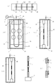
本発明の第1の実施の形態を図1に示す。図1は、図7に示した太陽電池の生産に用いられるプラズマCVD装置の一例を示す模式図である。
プラズマCVD装置は、図1(a)に示すように、ロードロック室10、加熱室20、第1プラズマCVD(PCVD)室30,第2PCVD室40及び冷却室50から構成され、各室はゲートバルブ61〜64を介して連結されている。
基板1は基板両面の薄膜形成面が露出するように基板ホルダ3に保持される。これは、例えば、図1(f)に示したように、基板の周辺端部を開口を有する平板4及び押え板5で挟持し、ネジ6で固定すればよい。
【0011】
複数の基板を保持した基板ホルダ3はキャリア2に取り付けられ(図1(e))、各室に敷設されたレール上を図1(a)の矢印の方向に搬送され、各室で所定の処理がなされる。即ち、基板ホルダはロードロック室10から加熱室20に搬送され、ここで赤外線ランプ等のヒータにより基板ホルダ3の両側から加熱処理され、所定温度まで加熱される。その後、第1PCVD室30、第2PCVD室40に順次搬送され、基板の両面にそれぞれn型a−Si膜及びp型a−Si膜が形成される。薄膜形成後、基板ホルダは冷却室50で所定温度まで冷却され、外部に取り出され、ITO等の透明導電膜及び集電電極の形成装置に搬送される。なお、冷却室の代わりにスパッタ室を連結し、a−Si膜形成後、すぐに透明導電膜を形成する装置構成とすることもできる。
【0012】
第1PCVD室30の構造を、図1(b)、(c)を用いて説明する。
図1(b)及び(c)は、室内部を、それぞれ正面から見た模式図及び搬送方向に向かって見た模式図である。PCVD室には薄膜形成用ガス(例えばSiH4/PH3ガス)の供給配管31及び排気口32が設けられ、室内部には中央で折り返した形状の誘導結合型電極33が配設されている。誘導結合型電極33の一端部の給電部34は、同軸ケーブル8を介して高周波電源7に接続され、他端部の接地部35は室壁に連結され接地されている。
【0013】
基板ホルダ3を搭載したキャリア2がPCVD室30に搬入されると、破線で示す位置にあった基板ホルダ固定治具36を閉じて実線で示すように基板ホルダを両側から当接させて固定する。この状態で、ガス供給配管31を通してSiH4/PH3ガスを室内に導入し、所定の圧力に設定した後、高周波電力を誘導結合型電極33に供給する。電極33に沿ってプラズマが発生し、電極33に面した基板表面にn型a−Si膜が堆積する。この際、基板成膜面の反対側にもガスは流れ込むがプラズマは基板ホルダ及び基板ホルダ固定治具により遮蔽され、裏側に回り込むことはなく、電極と反対側の基板表面に薄膜は形成されない。
【0014】
所定の膜厚が形成された後、電力の供給、ガス導入を停止して、室内を排気する。続いて、ゲートバルブ63を開け基板ホルダを第2PCVD室40に搬送する。図1(d)は、第2PCVD室内部を搬送方向に向かって見たときの模式図であり、誘導結合型電極43を基板ホルダに対して反対側の位置に配置した以外は、第1PCVD室と同じ構成である。第2PCVD室40に基板ホルダが搬送されると、基板ホルダ固定治具46が閉じ、基板ホルダは固定される。ここで、ガス供給配管41を通して、室内にSiH4/B2H6ガスを導入し、誘導結合型電極43に高周波電力を供給して、n型a−Si膜が形成された面と反対側の基板表面にp型a−Si膜が堆積する。このようにして、i型結晶シリコン基板の両側にp型a−Si及びn型a−Si膜が堆積し、pin接合が形成される。
以上のように、基板ホルダ3をキャリア2に載せて各室を順次搬送することにより、連続して基板の両面にp型及びn型a−Si膜を形成することが可能となる。
【0015】
上述したように、従来の平行平板型PCVD装置で膜厚均一性に優れた薄膜を形成するには、基板の成膜面と反対側に裏板を配置する必要があり、このため、両面成膜を行うには基板の反転工程が不可欠となり、しかも加熱・冷却工程等が2回必要となる。一方、本発明のプラズマCVD装置では、基板を反転する必要がなく、しかも基板の加熱、冷却工程が1回ですむため、処理室数の低減とともにスループットを向上させることができる。また、従来の装置で高スループット生産を行うには、ロードロック室、加熱室、PCVD室、冷却室が2組必要となるが、図1に示した実施の形態では、PCVD室は2つ必要とするものの、他の処理室は1つでよく、装置全体の設置面積及びコストを大幅に低減することができる。
【0016】
図1では、U字型の誘導結合型電極を示したが、中央で折り返した形状の誘導結合型電極は、U字型以外に例えば「コ」の字型のような矩形のものでも良い。ここで、給電部34及び接地部35と折り返し部との間の距離を、高周波の励振波長の略1/2又はその自然数倍とするのが好ましく、これにより安定した放電を発生・維持することができる。なお、折り返し部とは、U字型の場合、曲率を有する半円状の部分をいい、「コ」の字型の場合は2本の直線電極の間の直線部をいう。これらの電極は、例えば一本の棒材を折り曲げて一体に形成したものである必要はなく、例えば2本の直線状電極を金属板等で接続・固定した構造であっても良い。
さらに、本発明においては、棒状の電極を用いることもできる。この両端を給電部と接地部とし、給電部と接地部との距離を励振波長の略1/2又はその自然数倍とするのが好ましい。
【0017】
(第2の実施の形態)
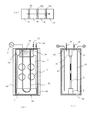
図1のプラズマCVD装置では、p型及びn型a−Si膜を異なるPCVD室で堆積する構成としたが、1つのPCVD室内で基板の両面に異なる薄膜を形成することも可能である。これを可能とする本発明の第2の実施の形態を図2に示す。装置全体としては、図2(a)に示したように、PCVD室が1つになった以外は、図1と同じ構成である。
【0018】
本実施の形態のプラズマCVD室30は、図2(b)、(c)に示したように、室内に2つの誘導結合型電極が配置され、それぞれの給電部34、34’が高周波電源に接続される。この2つの電極の間に、基板ホルダが搬入され、固定される。また、PCVD室には2種類の薄膜形成用ガス(SiH4/PH3ガス及びSiH4/B2H6ガス)の供給配管31,31’が連結されている。
【0019】
この装置では、PCVD室30に基板ホルダが搬送されてくると、まず、ガス供給配管31を通してSiH4/PH3ガスを室内に導入し、所定圧力に設定した後、電極33に高周波電力を供給して電極33に沿ってプラズマを発生させる。これにより、電極33に面した基板上にn型a−Si膜が堆積する。所定膜厚の薄膜が堆積した後、電力及びガスの供給を停止し、室内を排気する。
続いて、ガス供給配管31’を通してSiH4/B2H6ガスを導入し、同様にして電極33’に電力を供給してプラズマを発生させ、電極33’に面した基板上に所定膜厚のp型a−Si膜を堆積してpin接合を形成する。この後、冷却室50に搬送され、冷却された後外部に取り出される。
以上のようにして、同一室内で異なる種類の薄膜を形成することが可能となる。
【0020】
(第3の実施の形態)
図2の例では、n型a−Si膜形成後、p型a−Si膜を形成する構成としたが、2種類の薄膜を同時に形成することも可能である。同時成膜を可能とした第3の実施の形態を図3に示す。
プラズマCVD装置としては、図3に示したPCVD室を除いて、図2(a)と同じ構成である。本実施の形態のPCVD室は、次の点で図2(b)、(c)と異なる。即ち、図2では、n型又はp型a−Si膜の成膜空間に生成させるプラズマが反対側の成膜空間へ拡散し、p型又はn型成膜面に薄膜が形成されるのを防止する程度の遮蔽で十分であった。しかし、第3の実施形態では、基板ホルダ固定治具36の長さはできるだけ室の長さに近づけて、n型及びp型a−Si膜の成膜空間を相互のガスによる汚染(クロスコンタミネーション)を防ぐように分離する仕切板の役割を担わせる。また、室の長さは、基板ホルダ長さと同程度とし、隙間を小さくする。さらに、それぞれの成膜空間に対応して、2つのガス供給配管及び排気口32,32’を設けてある。この場合、排気口32及び32’の下流において排気ガスを集合し(32”)、排気系を一系列としている。
【0021】
2種類のガスを同時に導入すると、基板ホルダ及び仕切板と室内壁との間の隙間を通してガスが互いに流れ込む場合もあるが、p型及びn型のキャリア濃度はは膜中に含有されるP元素とB元素との濃度差によりほぼ決定される。従って、n型a−Si膜に含まれるP元素の数密度と比較して微量のB元素が混入しても、あるいはこれとは逆に、p型a−Si膜に含まれるB元素の数密度と比較して微量のP元素が混入しても、太陽電池特性には殆ど影響せず、所望の特性の太陽電池を得ることができる。
このように、同一室内で同時成膜を行うことにより、PCVD室の運転間隔をさらに短縮することができる。
なお、本実施の形態においては、2つ成膜空間のそれぞれに排気口を設けた構成としたが、例えば真空室底壁の中央部に排気口を1つ設ける構成とすることも可能である。また、仕切板についても、基板ホルダ固定治具を兼用したため、仕切板が基板ホルダに当接する構造としたが、基板ホルダ固定治具が必要ない場合あるいは別途仕切板を配置する場合は、必ずしも仕切板を基板ホルダに当接させる必要はなく、隙間があっても気流の調節等によりクロスコンタミネーションを抑制することができる。
【0022】
(第4の実施の形態)
上記実施の形態では、シリコン基板上に直接p型及びn型a−Si膜を形成する製造装置及び製造方法について述べてきたが、p/i接合及びi/n接合部の欠陥を低減して、太陽電池特性を向上させるためには、p型及びn型a−Si膜を形成する前に、基板両面の結晶シリコン上にi型a−Si膜を形成するのが好ましい。このための装置構成を、本発明の第4の実施の形態として、図4に示した。
【0023】
図4のプラズマCVD装置は、図2(a)のプラズマCVD装置のPCVD室30の前に、i型a−Si膜堆積用のPCVD室70を配設したものである。PCVD室70は、図2(b)、(c)と同じ構造を有し、SiH4ガスの供給配管を1つ連結したものである。SiH4ガスを導入後、2つの誘導結合型電極に同時に高周波電力を供給し、基板の両面に同じi型a−Si膜を堆積する。
n型及びp型a−Si膜の形成方法については、第2の実施の形態と同じである。
【0024】
(第5の実施の形態)
次に、本発明の第5の実施の形態として、極めて生産性の高いプラズマCVD装置を説明する。図1〜図4のプラズマCVD室は、1つの基板ホルダに保持された基板の両面に薄膜を連続して形成する構成であるが、より生産性を向上させるには、より多くの基板を基板ホルダに保持させ、かつ複数の基板ホルダを同時に処理できる構成とするのが好ましい。本発明の誘導結合型電極を用いたプラズマCVD室はこの拡張を容易に行うことができ、この量産対応の装置構成例を図5及び図6に示す。
【0025】
図5(a)、(b)は、図2の装置に対応する量産装置のPCVD室内部を、それぞれ正面から及び搬送方向に向かって見たときの模式図である。図5(a)に示すように、基板ホルダ面に対向して誘導結合型電極を同一平面内に複数配置したため、より大型の基板ホルダ(即ち、多数の基板を保持した基板ホルダ)に対して成膜処理を行うことができる。また、図5(b)に示すように、基板ホルダと電極列層とを交互に配置するだけで、1つの真空室内で多数の基板ホルダの成膜処理を行うことができる。
【0026】
即ち、ガス供給配管31を通してSiH4/PH3ガスを導入し、電極33,33”に電力を供給して、これらの基板に対向する基板面上にn型a−Si膜を形成する。続いて、ガスをSiH4/B2H6ガスに切り替え、電極33’、33'''に電力を供給して、これらの電極に面した基板面上にp型a−Si膜を形成する。ここで、電極基板面間距離は、30mm程度まで小さくすることができるため、小さな空間に多数の基板ホルダ及び電極を配置することができる。
なお、図5の構造は2つの薄膜を基板両面に別々に堆積する場合であるが、図3に示した同時成膜装置の場合も同様に構成すればよい。
【0027】
図6(a)、(b)は、図1の装置に対応する量産装置の第1及び第2PCVD室内部を、搬送方向に向かって見たときの模式図である。この場合は、2つの誘導結合型電極列層の間に2つの基板ホルダを配置する構成となる。
【0028】
以上、本発明を結晶シリコン基板の両面にa−Si膜を形成する方法及びその装置について述べてきたが、本発明は、これに限るものではなく、太陽電池以外の種々の用途、例えば、ガラスやプラスチック基板の表面改質等にも好適に適用される。
【0029】
【発明の効果】
本発明により、基板の裏板なしに均一性に優れた薄膜を形成することが可能となり、その結果、基板の反転工程が不要となり、しかも加熱・冷却工程等を減らすことができるため、両面成膜の生産性を著しく向上させることができる。
さらに、基板ホルダと誘導結合型電極を交互に配置した構成が可能となり、多数の基板を同時処理可能な極めて量産性に優れたプラズマCVD装置を提供することができる。
【図面の簡単な説明】
【図1】本発明の第1の実施の形態のプラズマCVD装置を示す模式図である。
【図2】第2の実施の形態のプラズマCVD装置を示す模式図である。
【図3】第3の実施の形態のプラズマCVD装置を示す模式図である。
【図4】第4の実施の形態のプラズマCVD装置を示す模式図である。
【図5】図2の量産対応装置を示す模式図である。
【図6】図1の量産対応装置を示す模式図である。
【図7】太陽電池の構造を示す模式図である。
【図8】従来のプラズマCVD装置を示す模式図である。
【符号の説明】
1 基板、
2 キャリア、
3 基板ホルダ、
7 高周波電源、
8 同軸ケーブル、
10、110 ロードロック室、
20、120 加熱室、
30、40、70、130 プラズマCVD室、
31、41 ガス供給配管、
32 排気口、
33、43 誘導結合型電極、
34 給電部、
35 接地部、
36 基板ホルダ固定治具、
50、140 冷却室、
61〜64、106 ゲートバルブ、
101 i型結晶Si、
102 p型a−Si、
103 n型a−Si、
104 透明電極、
105 集電電極。[0001]
BACKGROUND OF THE INVENTION
The present invention relates to a plasma CVD method and apparatus, and more particularly, to a plasma CVD method and apparatus capable of forming a thin film having excellent film thickness uniformity on both surfaces of a substrate.
[0002]
[Prior art]
Solar cells generally have a configuration in which a pn junction or a pin junction is formed on a substrate using Si, a compound semiconductor, or the like, and sunlight incident from the surface is photoelectrically converted. For this purpose, solar cells using light incident from the back side of the substrate have been proposed. This solar cell has the structure shown in FIG. 7, for example, and has a p-type amorphous Si (p-type a-Si)
[0003]
For the deposition of the a-Si film, for example, a parallel plate type plasma CVD apparatus shown in FIG. 8B is used. This apparatus includes a
[0004]
After the substrate temperature falls, the
Thereafter, a transparent conductive film such as ITO is formed on both sides of the
[0005]
[Problems to be solved by the invention]
As described above, a parallel plate type plasma CVD apparatus has been conventionally used for depositing an a-Si film. However, when a thin film is formed on a high-resistance substrate or an insulating substrate with a parallel plate type PCVD apparatus, if there is no back plate on the back surface of the substrate, high-frequency current is difficult to flow through the substrate, and the plasma density on the substrate surface is extremely high. descend. As a result, a difference in film thickness occurs between the central part and the peripheral part of the substrate, and there is a drawback that it is difficult to obtain a thin film with good film thickness uniformity. This becomes more noticeable as the substrate becomes larger. Therefore, in order to form a thin film with high film thickness uniformity, a back plate serving as a path for high-frequency current is indispensable, and thus there has been a problem that productivity of film formation on both sides of the substrate is remarkably reduced. That is, after forming a thin film on one side, it is necessary to take out the substrate and turn it over, and accordingly, the load lock chamber exhaust, the cooling chamber vent, and the substrate heating / cooling step are required twice.
Furthermore, in order to increase the throughput, two sets of the apparatus shown in FIG. 8B are required, which inevitably increases the size and cost of the entire production apparatus.
[0006]
In such a situation, an object of the present invention is to provide a plasma CVD method and apparatus capable of forming a thin film having excellent film thickness uniformity on both surfaces of a substrate without requiring a substrate inversion step.
[0007]
[Means for Solving the Problems]
The first gist of the present invention is that at least two inductively coupled electrodes having a power feeding part and a grounding part are arranged in a vacuum chamber provided with a gas supply port and an exhaust port, so that both surfaces of the substrate are exposed. A plasma CVD apparatus having a structure in which a substrate holder holding the outer peripheral edge of the substrate is inserted and disposed between the two inductively coupled electrodes, and a thin film forming gas is introduced from the gas supply system and a high frequency is supplied to the power supply unit. The present invention exists in a plasma CVD method and a plasma CVD apparatus characterized in that a power is supplied to generate plasma along the inductively coupled electrode to form a thin film on both surfaces of the substrate simultaneously or sequentially.
[0008]
Here, a second gas supply port is provided in the vacuum chamber, and different thin films are formed on both surfaces of the substrate by simultaneously switching between the introduction of two types of gas and the supply of power to the two inductively coupled electrodes. can do. Further, a partition plate is provided, and an air outlet is provided for each film formation space and an air outlet is provided so that different gases flow in the two film formation spaces divided by the partition plate and the substrate holder without being mixed with each other. Thus, different thin films can be simultaneously formed on both sides of the substrate.
Furthermore, by providing three or more electrode rows in which a plurality of the inductively coupled electrodes are arranged in the same plane and arranging the substrate holder between each of the electrode row layers, it is possible to achieve extremely high productivity. A high plasma CVD apparatus can be realized.
[0009]
The second gist of the present invention is a plasma CVD apparatus in which an inductively coupled electrode having a power feeding part and a grounding part is arranged inside, and two vacuum chambers provided with a gas supply port and an exhaust port are connected and arranged. The substrate holder holding the outer peripheral edge so that both surfaces of the substrate are exposed is transferred to the first vacuum chamber of the two vacuum chambers, and the first thin film forming gas is introduced through the gas supply port. A plasma is generated by supplying high-frequency power to a power feeding portion of the inductively coupled electrode, and after forming a first thin film on the surface of the substrate facing the inductively coupled electrode, the substrate holder is moved to the first thin film. Is transferred to the second vacuum chamber so that the surface opposite to the surface on which the surface is formed faces the inductively coupled electrode, and the second thin film forming gas is introduced through the gas supply port and the inductively coupled electrode A plasma is generated by supplying high-frequency power to the power feeding unit, and the first The thin film formed surfaces present in the plasma CVD method and a plasma CVD apparatus is characterized in that a configuration of forming a second thin film on the opposite substrate surface.
In order to obtain a device with high productivity, an electrode array in which a plurality of the inductively coupled electrodes are arranged in the same plane is connected to the first vacuum chamber (or the second vacuum layer) in an n layer (n is (An integer of 2 or more), (n-1) layers may be provided in the second vacuum chamber (or the first vacuum layer), and two substrate holders may be disposed between the electrode array layers.
[0010]
DETAILED DESCRIPTION OF THE INVENTION
Hereinafter, embodiments of the present invention will be described in detail with reference to the drawings.
(First embodiment)
A first embodiment of the present invention is shown in FIG. FIG. 1 is a schematic diagram showing an example of a plasma CVD apparatus used for production of the solar cell shown in FIG.
As shown in FIG. 1A, the plasma CVD apparatus includes a
The
[0011]
A
[0012]
The structure of the
FIGS. 1B and 1C are a schematic view of the interior of the room viewed from the front and a schematic view of the interior as viewed in the transport direction, respectively. The PCVD chamber is provided with a
[0013]
When the
[0014]
After the predetermined film thickness is formed, power supply and gas introduction are stopped, and the room is exhausted. Subsequently, the
As described above, it is possible to continuously form the p-type and n-type a-Si films on both surfaces of the substrate by placing the
[0015]
As described above, in order to form a thin film having excellent film thickness uniformity with a conventional parallel plate type PCVD apparatus, it is necessary to dispose a back plate on the side opposite to the film formation surface of the substrate. In order to form a film, the inversion process of the substrate is indispensable, and the heating / cooling process is required twice. On the other hand, in the plasma CVD apparatus of the present invention, it is not necessary to invert the substrate, and the substrate heating and cooling steps are required only once, so that the number of processing chambers can be reduced and the throughput can be improved. In addition, in order to perform high-throughput production with the conventional apparatus, two sets of a load lock chamber, a heating chamber, a PCVD chamber, and a cooling chamber are required. In the embodiment shown in FIG. 1, two PCVD chambers are required. However, the number of other processing chambers may be one, and the installation area and cost of the entire apparatus can be greatly reduced.
[0016]
Although FIG. 1 shows a U-shaped inductively coupled electrode, the inductively coupled electrode folded in the center may have a rectangular shape such as a “U” shape in addition to the U shape. Here, it is preferable that the distance between the
Furthermore, in the present invention, a rod-shaped electrode can also be used. It is preferable that the both ends be a power feeding part and a grounding part, and the distance between the power feeding part and the grounding part be approximately ½ of the excitation wavelength or a natural number thereof.
[0017]
(Second Embodiment)
In the plasma CVD apparatus of FIG. 1, the p-type and n-type a-Si films are deposited in different PCVD chambers. However, it is possible to form different thin films on both surfaces of the substrate in one PCVD chamber. FIG. 2 shows a second embodiment of the present invention that enables this. As shown in FIG. 2A, the entire apparatus has the same configuration as that of FIG. 1 except that there is only one PCVD chamber.
[0018]
In the
[0019]
In this apparatus, when the substrate holder is transferred to the
Subsequently, SiH 4 / B 2 H 6 gas is introduced through the
As described above, different types of thin films can be formed in the same chamber.
[0020]
(Third embodiment)
In the example of FIG. 2, the p-type a-Si film is formed after the n-type a-Si film is formed. However, two types of thin films can be formed simultaneously. 3rd Embodiment which enabled simultaneous film-forming is shown in FIG.
The plasma CVD apparatus has the same configuration as FIG. 2A except for the PCVD chamber shown in FIG. The PCVD chamber of this embodiment is different from FIGS. 2B and 2C in the following points. That is, in FIG. 2, the plasma generated in the deposition space of the n-type or p-type a-Si film diffuses into the deposition space on the opposite side, and a thin film is formed on the p-type or n-type deposition surface. A degree of shielding was sufficient. However, in the third embodiment, the length of the substrate
[0021]
If two kinds of gases are introduced simultaneously, the gases may flow into each other through a gap between the substrate holder and the partition plate and the interior wall, but the p-type and n-type carrier concentrations are the P element contained in the film. And the concentration difference between the B element and the B element. Therefore, even if a trace amount of B element is mixed as compared with the number density of P element contained in the n-type a-Si film, or conversely, the number of B element contained in the p-type a-Si film. Even if a small amount of P element is mixed as compared with the density, the solar cell characteristics are hardly affected, and a solar cell having desired characteristics can be obtained.
In this way, by performing simultaneous film formation in the same chamber, the operation interval of the PCVD chamber can be further shortened.
In the present embodiment, an exhaust port is provided in each of the two film formation spaces. However, for example, a configuration in which one exhaust port is provided in the central portion of the vacuum chamber bottom wall is also possible. . Also, since the partition plate is also used as the substrate holder fixing jig, the partition plate is in contact with the substrate holder. However, when the substrate holder fixing jig is not required or when a separate partition plate is provided, the partition plate is not necessarily partitioned. There is no need to bring the plate into contact with the substrate holder, and even if there is a gap, cross contamination can be suppressed by adjusting the airflow.
[0022]
(Fourth embodiment)
In the above embodiment, a manufacturing apparatus and a manufacturing method for directly forming p-type and n-type a-Si films on a silicon substrate have been described. However, defects in p / i junctions and i / n junctions are reduced. In order to improve the solar cell characteristics, it is preferable to form i-type a-Si films on crystalline silicon on both surfaces of the substrate before forming the p-type and n-type a-Si films. An apparatus configuration for this purpose is shown in FIG. 4 as a fourth embodiment of the present invention.
[0023]
In the plasma CVD apparatus of FIG. 4, a
The method for forming the n-type and p-type a-Si films is the same as in the second embodiment.
[0024]
(Fifth embodiment)
Next, a highly productive plasma CVD apparatus will be described as a fifth embodiment of the present invention. The plasma CVD chamber of FIGS. 1 to 4 is configured to continuously form a thin film on both surfaces of a substrate held by one substrate holder, but in order to improve productivity, more substrates are used. It is preferable that the holder be held and a plurality of substrate holders be processed at the same time. The plasma CVD chamber using the inductively coupled electrode of the present invention can be easily expanded, and an example of the apparatus configuration for mass production is shown in FIGS.
[0025]
FIGS. 5A and 5B are schematic views of the inside of the PCVD chamber of the mass production apparatus corresponding to the apparatus of FIG. 2 when viewed from the front and in the transport direction. As shown in FIG. 5 (a), since a plurality of inductively coupled electrodes are arranged in the same plane so as to face the substrate holder surface, a larger substrate holder (that is, a substrate holder holding a large number of substrates) is used. A film forming process can be performed. Further, as shown in FIG. 5 (b), a number of substrate holders can be formed in a single vacuum chamber simply by alternately arranging the substrate holders and electrode row layers.
[0026]
That is, SiH 4 / PH 3 gas is introduced through the
5 shows a case where two thin films are separately deposited on both surfaces of the substrate, but the simultaneous film forming apparatus shown in FIG. 3 may be configured similarly.
[0027]
FIGS. 6A and 6B are schematic views of the first and second PCVD chambers of the mass production apparatus corresponding to the apparatus of FIG. 1 as viewed in the transport direction. In this case, two substrate holders are arranged between the two inductively coupled electrode array layers.
[0028]
As mentioned above, although this invention has described the method and apparatus for forming an a-Si film on both surfaces of a crystalline silicon substrate, the present invention is not limited to this, and various uses other than solar cells, for example, glass It is also suitably applied to surface modification of plastic substrates.
[0029]
【The invention's effect】
According to the present invention, it is possible to form a thin film having excellent uniformity without a back plate of the substrate. As a result, the inversion process of the substrate is not necessary, and the heating / cooling process can be reduced. Membrane productivity can be significantly improved.
Furthermore, a configuration in which substrate holders and inductively coupled electrodes are alternately arranged is possible, and a plasma CVD apparatus excellent in mass productivity that can simultaneously process a large number of substrates can be provided.
[Brief description of the drawings]
FIG. 1 is a schematic diagram showing a plasma CVD apparatus according to a first embodiment of the present invention.
FIG. 2 is a schematic diagram showing a plasma CVD apparatus according to a second embodiment.
FIG. 3 is a schematic diagram showing a plasma CVD apparatus according to a third embodiment.
FIG. 4 is a schematic diagram showing a plasma CVD apparatus according to a fourth embodiment.
FIG. 5 is a schematic diagram showing the apparatus for mass production shown in FIG.
6 is a schematic diagram showing the mass production support device of FIG. 1. FIG.
FIG. 7 is a schematic diagram showing the structure of a solar cell.
FIG. 8 is a schematic view showing a conventional plasma CVD apparatus.
[Explanation of symbols]
1 substrate,
2 career,
3 Substrate holder,
7 high frequency power supply,
8 Coaxial cable,
10, 110 Load lock room,
20, 120 heating chamber,
30, 40, 70, 130 Plasma CVD chamber,
31, 41 Gas supply piping,
32 Exhaust port,
33, 43 Inductively coupled electrodes,
34 Power supply unit,
35 Grounding part,
36 Substrate holder fixing jig,
50, 140 cooling chamber,
61-64, 106 gate valve,
101 i-type crystal Si,
102 p-type a-Si,
103 n-type a-Si,
104 transparent electrode,
105 Current collecting electrode.
Claims (5)
前記誘導結合電極を複数個、同一平面内に配置した電極列を、前記第1の真空室にn層(nは2以上の整数)、前記第2の真空室に(n−1)層設け、
前記第1の真空室内におけるn層の前記電極列のうち隣り合う電極列の間に基板ホルダが2個ずつ位置するように2(n−1)個の前記基板ホルダを前記第1の真空室に搬送し、ガス供給口を介して第1の薄膜形成用ガスを導入するとともに給電部に高周波電力を供給してプラズマを発生させ、誘導結合型電極に面した基板の表面上に第1の薄膜を形成した後、
前記第1の薄膜が形成された面と反対側の基板の表面が誘導結合型電極に面するように、前記基板ホルダを前記第2の真空室に搬送し、ガス供給口を介して第2の薄膜形成ガスを導入するとともに給電部に高周波電力を供給してプラズマを発生させ、前記第1の薄膜が形成された表面とは反対側の基板の表面に第2の薄膜を形成する構成としたことを特徴とするプラズマCVD装置。The first and second vacuum chambers are connected via a gate valve, each of the vacuum chambers is provided with a gas supply port and an exhaust port, and an inductively coupled electrode having a power feeding portion and a grounding portion therein, and both surfaces of the substrate are exposed. A plasma CVD apparatus in which a substrate holder holding an outer peripheral edge portion is arranged,
An electrode array in which a plurality of the inductive coupling electrodes are arranged in the same plane is provided with n layers (n is an integer of 2 or more) in the first vacuum chamber and (n-1) layers in the second vacuum chamber. ,
In the first vacuum chamber, 2 (n-1) substrate holders are arranged in the first vacuum chamber so that two substrate holders are positioned between adjacent electrode rows among the n electrode rows in the first vacuum chamber. The first thin film forming gas is introduced through the gas supply port and high-frequency power is supplied to the power supply unit to generate plasma, and the first surface is formed on the surface of the substrate facing the inductively coupled electrode. After forming the thin film ,
As the front surface of the substrate opposite to the first thin film is formed faces facing the inductive coupling type electrode, conveying the substrate holder into the second vacuum chamber, first through a gas supply port with introducing two thin film forming gas by supplying high frequency power to generate plasma to a power source, wherein the first thin film is formed surface to form a second thin film on the surface of the substrate opposite configuration A plasma CVD apparatus characterized by the above.
前記誘導結合電極を複数個、同一平面内に配置した電極列を、前記第2の真空室にn層(nは2以上の整数)、前記第1の真空室に(n−1)層設け、
一対の前記基板ホルダーの間に前記第1の真空室内における前記各電極列が一つずつ位置するように2(n−1)個の基板ホルダーを前記第1の真空室に搬送し、ガス供給口を介して第1の薄膜形成用ガスを導入するとともに給電部に高周波電力を供給してプラズマを発生させ、誘導結合型電極に面した基板の表面上に第1の薄膜を形成した後、
前記第1の薄膜が形成された面と反対側の基板の表面が誘導結合型電極に面するように、前記基板ホルダを前記第2の真空室に搬送し、ガス供給口を介して第2の薄膜形成ガスを導入するとともに給電部に高周波電力を供給してプラズマを発生させ、前記第1の薄膜が形成された表面とは反対側の基板の表面に第2の薄膜を形成する構成としたことを特徴とするプラズマCVD装置。The first and second vacuum chambers are connected via a gate valve, each of the vacuum chambers is provided with a gas supply port and an exhaust port, and an inductively coupled electrode having a power feeding portion and a grounding portion therein, and both surfaces of the substrate are exposed. A plasma CVD apparatus in which a substrate holder holding an outer peripheral edge portion is arranged,
An electrode array in which a plurality of the inductively coupled electrodes are arranged in the same plane is provided with n layers (n is an integer of 2 or more) in the second vacuum chamber and (n-1) layers in the first vacuum chamber. ,
2 (n-1) substrate holders are transported to the first vacuum chamber so that each of the electrode rows in the first vacuum chamber is positioned one by one between the pair of substrate holders , and gas is supplied. After introducing the first gas for forming a thin film through the mouth and supplying high-frequency power to the power supply unit to generate plasma, and forming the first thin film on the surface of the substrate facing the inductively coupled electrode ,
The substrate holder is transported to the second vacuum chamber so that the surface of the substrate opposite to the surface on which the first thin film is formed faces the inductively coupled electrode, and the second holder is connected to the second vacuum chamber via the gas supply port. And forming a second thin film on the surface of the substrate opposite to the surface on which the first thin film is formed, by introducing high-frequency power to the power feeding section and generating plasma. A plasma CVD apparatus characterized by that.
基板両面が露出するように外周端部を保持した基板ホルダを2(n−1)個、搭載したキャリアを、前記第1の真空室内におけるn層の前記電極列のうち隣り合う電極列の間に基板ホルダが2個ずつ入るように前記第1の真空室に搬送し、ガス供給口を介して第1の薄膜形成用ガスを導入するとともに誘導結合型電極の給電部に高周波電力を供給してプラズマを発生させ、該誘導結合型電極に面した基板の表面上に第1の薄膜を形成した後、
前記第1の薄膜が形成された面と反対側の基板の表面が誘導結合型電極に面するように、前記基板ホルダが搭載された前記キャリアを前記第2の真空室に搬送し、ガス供給口を介して第2の薄膜形成ガスを導入するとともに誘導結合型電極の給電部に高周波電力を供給してプラズマを発生させ、前記第1の薄膜が形成された表面とは反対側の基板の表面に第2の薄膜を形成することを特徴とする太陽電池の製造方法。The first and second vacuum chamber that includes a gas supply port and the exhaust port is provided, the inductive coupling type electrode having a grounding portion and the feeding portion plurality, the electrode array disposed in the same plane, the first N layers (n is an integer of 2 or more) in the vacuum chamber, (n-1) layers are arranged in the second vacuum chamber ,
2 (n-1) substrate holders holding outer peripheral edges so that both surfaces of the substrate are exposed, and a carrier mounted between adjacent electrode rows among the electrode rows of n layers in the first vacuum chamber. The substrate holder is transferred to the first vacuum chamber so that two substrate holders can be inserted into each , and the first thin film forming gas is introduced through the gas supply port, and high-frequency power is supplied to the power feeding portion of the inductively coupled electrode. And generating a first thin film on the surface of the substrate facing the inductively coupled electrode ,
Wherein as the front surface of the substrate opposite the first thin film is formed faces facing the inductive coupling type electrode, and transport the carrier in which the substrate holder is mounted on said second vacuum chamber, gas A substrate opposite to the surface on which the first thin film is formed by introducing a second thin film forming gas through the supply port and supplying high frequency power to the power feeding portion of the inductively coupled electrode to generate plasma. Forming a second thin film on the surface of the solar cell.
基板両面が露出するように外周端部を保持した基板ホルダを2(n−1)個、搭載したキャリアを、一対の前記基板ホルダーの間に前記第1の真空室内における前記各電極列が一つずつ位置するように前記第1の真空室に搬送し、ガス供給口を介して第1の薄膜形成用ガスを導入するとともに誘導結合型電極の給電部に高周波電力を供給してプラズマを発生させ、該誘導結合型電極に面した基板の表面上に第1の薄膜を形成した後、
前記第1の薄膜が形成された面と反対側の基板の表面が誘導結合型電極に面するように、前記基板ホルダが搭載された前記キャリアを前記第2の真空室に搬送し、ガス供給口を介して第2の薄膜形成ガスを導入するとともに誘導結合型電極の給電部に高周波電力を供給してプラズマを発生させ、前記第1の薄膜が形成された表面とは反対側の基板の表面に第2の薄膜を形成することを特徴とする太陽電池の製造方法。First and second vacuum chambers having a gas supply port and an exhaust port are provided, and an electrode array in which a plurality of inductively coupled electrodes having a power feeding unit and a grounding unit are arranged in the same plane is provided as the second electrode N layers (n is an integer of 2 or more) in the vacuum chamber, (n-1) layers are arranged in the first vacuum chamber ,
Each of the electrode rows in the first vacuum chamber is placed between a pair of substrate holders with 2 (n-1) substrate holders holding the outer peripheral edges so that both surfaces of the substrate are exposed. Transfer to the first vacuum chamber to be positioned one by one , introduce the first thin film forming gas through the gas supply port, and supply high frequency power to the power supply part of the inductively coupled electrode to generate plasma And forming a first thin film on the surface of the substrate facing the inductively coupled electrode ,
The carrier on which the substrate holder is mounted is transported to the second vacuum chamber so that the surface of the substrate opposite to the surface on which the first thin film is formed faces the inductively coupled electrode, and the gas supply The second thin film forming gas is introduced through the mouth and high frequency power is supplied to the power feeding portion of the inductively coupled electrode to generate plasma, and the substrate on the side opposite to the surface on which the first thin film is formed . A method for producing a solar cell, comprising forming a second thin film on a surface.
Priority Applications (9)
| Application Number | Priority Date | Filing Date | Title |
|---|---|---|---|
| JP2001012702A JP4770029B2 (en) | 2001-01-22 | 2001-01-22 | Plasma CVD apparatus and solar cell manufacturing method |
| ES02715845T ES2430190T3 (en) | 2001-01-22 | 2002-01-21 | Device for plasma CVD |
| CNB028039971A CN100349261C (en) | 2001-01-22 | 2002-01-21 | Method and device for plasma CVD |
| AU2002225452A AU2002225452B2 (en) | 2001-01-22 | 2002-01-21 | Method and device for plasma CVD |
| PCT/JP2002/000381 WO2002058121A1 (en) | 2001-01-22 | 2002-01-21 | Method and device for plasma cvd |
| EP02715845.0A EP1359611B1 (en) | 2001-01-22 | 2002-01-21 | Device for plasma CVD |
| US10/466,853 US7047903B2 (en) | 2001-01-22 | 2002-01-21 | Method and device for plasma CVD |
| KR1020037009681A KR100777956B1 (en) | 2001-01-22 | 2002-01-21 | Method and device for plasma cvd |
| TW091100926A TW563185B (en) | 2001-01-22 | 2002-01-22 | Method and device for plasma CVD |
Applications Claiming Priority (1)
| Application Number | Priority Date | Filing Date | Title |
|---|---|---|---|
| JP2001012702A JP4770029B2 (en) | 2001-01-22 | 2001-01-22 | Plasma CVD apparatus and solar cell manufacturing method |
Publications (2)
| Publication Number | Publication Date |
|---|---|
| JP2002217119A JP2002217119A (en) | 2002-08-02 |
| JP4770029B2 true JP4770029B2 (en) | 2011-09-07 |
Family
ID=18879672
Family Applications (1)
| Application Number | Title | Priority Date | Filing Date |
|---|---|---|---|
| JP2001012702A Expired - Lifetime JP4770029B2 (en) | 2001-01-22 | 2001-01-22 | Plasma CVD apparatus and solar cell manufacturing method |
Country Status (9)
| Country | Link |
|---|---|
| US (1) | US7047903B2 (en) |
| EP (1) | EP1359611B1 (en) |
| JP (1) | JP4770029B2 (en) |
| KR (1) | KR100777956B1 (en) |
| CN (1) | CN100349261C (en) |
| AU (1) | AU2002225452B2 (en) |
| ES (1) | ES2430190T3 (en) |
| TW (1) | TW563185B (en) |
| WO (1) | WO2002058121A1 (en) |
Families Citing this family (32)
| Publication number | Priority date | Publication date | Assignee | Title |
|---|---|---|---|---|
| JP4029615B2 (en) * | 1999-09-09 | 2008-01-09 | 株式会社Ihi | Internal electrode type plasma processing apparatus and plasma processing method |
| ES2336303T3 (en) * | 2000-05-17 | 2010-04-12 | Ihi Corporation | APPLIANCE AND PROCEDURE OF CVD BY PLASMA. |
| JP4120546B2 (en) * | 2002-10-04 | 2008-07-16 | 株式会社Ihi | Thin film forming method and apparatus, solar cell manufacturing method and apparatus, and solar cell |
| JP4306218B2 (en) | 2002-10-18 | 2009-07-29 | 株式会社Ihi | Thin film forming system |
| JP4306322B2 (en) * | 2003-05-02 | 2009-07-29 | 株式会社Ihi | Substrate transfer device for thin film forming equipment |
| JP4450664B2 (en) * | 2003-06-02 | 2010-04-14 | 東京エレクトロン株式会社 | Substrate processing apparatus and substrate transfer method |
| JP4671361B2 (en) * | 2004-03-26 | 2011-04-13 | 日新電機株式会社 | Plasma generator |
| CN101027423B (en) * | 2004-08-30 | 2010-12-01 | 株式会社爱发科 | Film forming equipment |
| JP2008520108A (en) * | 2004-11-10 | 2008-06-12 | デイスター テクノロジーズ,インコーポレイティド | Vertical production of photovoltaic devices |
| CN101094726A (en) * | 2004-11-10 | 2007-12-26 | 德斯塔尔科技公司 | Thermal process for creation of an in-situ junction layer in cigs |
| KR100909750B1 (en) | 2005-03-01 | 2009-07-29 | 가부시키가이샤 히다치 고쿠사이 덴키 | Substrate processing apparatus and semiconductor device manufacturing method |
| US20070264842A1 (en) * | 2006-05-12 | 2007-11-15 | Samsung Electronics Co., Ltd. | Insulation film deposition method for a semiconductor device |
| US7845310B2 (en) * | 2006-12-06 | 2010-12-07 | Axcelis Technologies, Inc. | Wide area radio frequency plasma apparatus for processing multiple substrates |
| JP5028193B2 (en) * | 2007-09-05 | 2012-09-19 | 株式会社日立ハイテクノロジーズ | Method for conveying object to be processed in semiconductor manufacturing apparatus |
| US20110189384A1 (en) * | 2008-06-06 | 2011-08-04 | Ulvac, Inc. | Thin-film solar cell manufacturing apparatus |
| KR101215588B1 (en) * | 2008-06-06 | 2012-12-26 | 가부시키가이샤 아루박 | Apparatus for manufacturing thin film solar cell |
| WO2009148087A1 (en) * | 2008-06-06 | 2009-12-10 | 株式会社アルバック | Apparatus for manufacturing thin film solar cell |
| TWI432100B (en) * | 2009-11-25 | 2014-03-21 | Ind Tech Res Inst | Plasma generating aparatus |
| CN102315087A (en) * | 2010-06-30 | 2012-01-11 | 财团法人工业技术研究院 | Surface treatment device and method thereof |
| US9293356B2 (en) | 2011-06-03 | 2016-03-22 | Tel Nexx, Inc. | Parallel single substrate processing system |
| KR101288130B1 (en) * | 2011-07-13 | 2013-07-19 | 삼성디스플레이 주식회사 | Vapor deposition apparatus, method for vapor deposition and method for manufacturing organic light emitting display apparatus |
| WO2013030959A1 (en) * | 2011-08-30 | 2013-03-07 | 三菱電機株式会社 | Plasma film forming apparatus and plasma film forming method |
| JP2013072132A (en) * | 2011-09-29 | 2013-04-22 | Ulvac Japan Ltd | Film-forming apparatus |
| JP5840095B2 (en) * | 2011-10-31 | 2016-01-06 | 三菱電機株式会社 | Solar cell manufacturing apparatus and solar cell manufacturing method |
| CN103094413B (en) * | 2011-10-31 | 2016-03-23 | 三菱电机株式会社 | The manufacturing installation of solar cell, solar cell and manufacture method thereof |
| JP5018994B1 (en) * | 2011-11-09 | 2012-09-05 | 日新電機株式会社 | Plasma processing equipment |
| CN103466954A (en) * | 2012-06-08 | 2013-12-25 | 冠晶光电股份有限公司 | Partition board type deposition apparatus |
| WO2014064779A1 (en) * | 2012-10-24 | 2014-05-01 | 株式会社Jcu | Plasma treatment device and method |
| JP6185304B2 (en) * | 2013-06-28 | 2017-08-23 | 株式会社カネカ | Crystalline silicon photoelectric conversion device and manufacturing method thereof |
| CN106531847A (en) * | 2016-12-29 | 2017-03-22 | 常州大学 | Black silicon based tunneling contact solar cell online preparation equipment |
| CN106531848A (en) * | 2016-12-30 | 2017-03-22 | 常州大学 | Black silicon-based on-line preparation equipment of tunneling contact solar cell |
| JP6920676B2 (en) * | 2017-04-19 | 2021-08-18 | パナソニックIpマネジメント株式会社 | Fine particle production equipment and fine particle production method |
Family Cites Families (39)
| Publication number | Priority date | Publication date | Assignee | Title |
|---|---|---|---|---|
| CN1027549C (en) * | 1985-10-14 | 1995-02-01 | 株式会社半导体能源研究所 | Microwave enhanced CVD system under magnetic field |
| JPS63276222A (en) * | 1987-05-08 | 1988-11-14 | Mitsubishi Electric Corp | Thin film deposition system |
| JPH0313578A (en) * | 1989-06-09 | 1991-01-22 | Mitsubishi Electric Corp | Thin film forming device |
| US6068784A (en) * | 1989-10-03 | 2000-05-30 | Applied Materials, Inc. | Process used in an RF coupled plasma reactor |
| JPH03122274A (en) * | 1989-10-05 | 1991-05-24 | Asahi Glass Co Ltd | Production of thin film and device thereof |
| EP0428161B1 (en) * | 1989-11-15 | 1999-02-17 | Kokusai Electric Co., Ltd. | Dry process system |
| JP2785442B2 (en) | 1990-05-15 | 1998-08-13 | 三菱重工業株式会社 | Plasma CVD equipment |
| JP2989279B2 (en) | 1991-01-21 | 1999-12-13 | 三菱重工業株式会社 | Plasma CVD equipment |
| US5324360A (en) * | 1991-05-21 | 1994-06-28 | Canon Kabushiki Kaisha | Method for producing non-monocrystalline semiconductor device and apparatus therefor |
| US6063233A (en) * | 1991-06-27 | 2000-05-16 | Applied Materials, Inc. | Thermal control apparatus for inductively coupled RF plasma reactor having an overhead solenoidal antenna |
| US5477975A (en) * | 1993-10-15 | 1995-12-26 | Applied Materials Inc | Plasma etch apparatus with heated scavenging surfaces |
| DE4136297A1 (en) | 1991-11-04 | 1993-05-06 | Plasma Electronic Gmbh, 7024 Filderstadt, De | Localised plasma prodn. in treatment chamber - using microwave generator connected to coupling device which passes through the wall of the chamber without using a coupling window |
| US5824158A (en) * | 1993-06-30 | 1998-10-20 | Kabushiki Kaisha Kobe Seiko Sho | Chemical vapor deposition using inductively coupled plasma and system therefor |
| JPH0794421A (en) | 1993-09-21 | 1995-04-07 | Anelva Corp | Manufacture of amorphous silicon thin film |
| KR100276736B1 (en) * | 1993-10-20 | 2001-03-02 | 히가시 데쓰로 | Plasma processing equipment |
| US5525159A (en) * | 1993-12-17 | 1996-06-11 | Tokyo Electron Limited | Plasma process apparatus |
| DE19503205C1 (en) | 1995-02-02 | 1996-07-11 | Muegge Electronic Gmbh | Device for generating a plasma in low pressure container e.g. for hardware items surface treatment by plasma etching and plasma deposition |
| JPH09106899A (en) * | 1995-10-11 | 1997-04-22 | Anelva Corp | Plasma cvd device and method, and dry etching device and method |
| JP3268965B2 (en) * | 1995-10-13 | 2002-03-25 | 三洋電機株式会社 | Apparatus and method for forming a semiconductor film on a substrate |
| KR970064327A (en) * | 1996-02-27 | 1997-09-12 | 모리시다 요이치 | High frequency power applying device, plasma generating device, plasma processing device, high frequency power applying method, plasma generating method and plasma processing method |
| JPH09268370A (en) | 1996-04-03 | 1997-10-14 | Canon Inc | Plasma cvd system and formation of deposited film by plasma cvd |
| JP3544076B2 (en) | 1996-08-22 | 2004-07-21 | キヤノン株式会社 | Plasma CVD apparatus and method for forming deposited film by plasma CVD |
| JP3207770B2 (en) * | 1996-11-01 | 2001-09-10 | 株式会社ボッシュオートモーティブシステム | Plasma CVD equipment |
| JPH11131244A (en) | 1997-10-28 | 1999-05-18 | Canon Inc | High-frequency electrode for plasma generation, plasma cvd device composed by the electrode, and plasma cvd method |
| JPH10265212A (en) | 1997-03-26 | 1998-10-06 | Nippon Telegr & Teleph Corp <Ntt> | Production of microcrystal and polycrystal silicon thin films |
| EP0908923B1 (en) * | 1997-10-10 | 2003-04-02 | European Community | Apparatus to produce large inductive plasma for plasma processing |
| EP0908921A1 (en) | 1997-10-10 | 1999-04-14 | European Community | Process chamber for plasma enhanced chemical vapour deposition and apparatus employing said process chamber |
| KR19990035509A (en) * | 1997-10-31 | 1999-05-15 | 윤종용 | Poly film etching method of semiconductor device |
| JP3501668B2 (en) | 1997-12-10 | 2004-03-02 | キヤノン株式会社 | Plasma CVD method and plasma CVD apparatus |
| DE19801366B4 (en) | 1998-01-16 | 2008-07-03 | Applied Materials Gmbh & Co. Kg | Device for generating plasma |
| JPH11317299A (en) | 1998-02-17 | 1999-11-16 | Toshiba Corp | High frequency discharge method, its device, and high frequency processing device |
| KR100263611B1 (en) * | 1998-03-30 | 2000-09-01 | 윤종용 | Method for trench fabrication |
| KR100265796B1 (en) * | 1998-05-26 | 2000-10-02 | 윤종용 | Fabrication method for porous film using icp etching technique |
| JP3844274B2 (en) * | 1998-06-25 | 2006-11-08 | 独立行政法人産業技術総合研究所 | Plasma CVD apparatus and plasma CVD method |
| JP2000345351A (en) * | 1999-05-31 | 2000-12-12 | Anelva Corp | Plasma cvd device |
| JP3836636B2 (en) | 1999-07-27 | 2006-10-25 | 独立行政法人科学技術振興機構 | Plasma generator |
| JP4029615B2 (en) * | 1999-09-09 | 2008-01-09 | 株式会社Ihi | Internal electrode type plasma processing apparatus and plasma processing method |
| KR100757717B1 (en) * | 2000-04-13 | 2007-09-11 | 도꾸리쯔교세이호진 상교기쥬쯔 소고겡뀨죠 | Thin film forming method, thin film forming apparatus and solar cell |
| ES2336303T3 (en) * | 2000-05-17 | 2010-04-12 | Ihi Corporation | APPLIANCE AND PROCEDURE OF CVD BY PLASMA. |
-
2001
- 2001-01-22 JP JP2001012702A patent/JP4770029B2/en not_active Expired - Lifetime
-
2002
- 2002-01-21 EP EP02715845.0A patent/EP1359611B1/en not_active Expired - Lifetime
- 2002-01-21 ES ES02715845T patent/ES2430190T3/en not_active Expired - Lifetime
- 2002-01-21 WO PCT/JP2002/000381 patent/WO2002058121A1/en active Application Filing
- 2002-01-21 AU AU2002225452A patent/AU2002225452B2/en not_active Ceased
- 2002-01-21 US US10/466,853 patent/US7047903B2/en not_active Expired - Fee Related
- 2002-01-21 CN CNB028039971A patent/CN100349261C/en not_active Expired - Fee Related
- 2002-01-21 KR KR1020037009681A patent/KR100777956B1/en not_active IP Right Cessation
- 2002-01-22 TW TW091100926A patent/TW563185B/en not_active IP Right Cessation
Also Published As
| Publication number | Publication date |
|---|---|
| US20040053479A1 (en) | 2004-03-18 |
| CN100349261C (en) | 2007-11-14 |
| AU2002225452B2 (en) | 2006-08-10 |
| JP2002217119A (en) | 2002-08-02 |
| KR100777956B1 (en) | 2007-11-21 |
| CN1489782A (en) | 2004-04-14 |
| TW563185B (en) | 2003-11-21 |
| EP1359611A1 (en) | 2003-11-05 |
| WO2002058121A1 (en) | 2002-07-25 |
| EP1359611B1 (en) | 2013-09-11 |
| EP1359611A4 (en) | 2007-01-10 |
| KR20030070128A (en) | 2003-08-27 |
| US7047903B2 (en) | 2006-05-23 |
| ES2430190T3 (en) | 2013-11-19 |
Similar Documents
| Publication | Publication Date | Title |
|---|---|---|
| JP4770029B2 (en) | Plasma CVD apparatus and solar cell manufacturing method | |
| US4492716A (en) | Method of making non-crystalline semiconductor layer | |
| US8865259B2 (en) | Method and system for inline chemical vapor deposition | |
| CN102598240A (en) | Vertically integrated processing chamber | |
| JPS6015918A (en) | External isolating module | |
| US20090029502A1 (en) | Apparatuses and methods of substrate temperature control during thin film solar manufacturing | |
| KR101486937B1 (en) | Atomic layer deposition apparatus and method thereof | |
| US20110262641A1 (en) | Inline chemical vapor deposition system | |
| JP2011527729A (en) | Method and system for manufacturing solar cells utilizing atmospheric pressure plasma chemical vapor deposition | |
| JP2616760B2 (en) | Plasma gas phase reactor | |
| JPS59177922A (en) | Process gas introducing and feeding system | |
| JP2014523479A (en) | In-line chemical vapor deposition method and system | |
| JPH11121381A (en) | Plasma chemical vapor depositing device | |
| JP2001323376A (en) | Equipment for depositing film | |
| JPH08195348A (en) | Semiconductor device manufacturing equipment | |
| JPH08260149A (en) | Reduced pressure surface treating device and apparatus for producing solar battery | |
| JPH0522376B2 (en) | ||
| JPH09213636A (en) | This film forming device | |
| JP2815711B2 (en) | Thin-film semiconductor device manufacturing equipment | |
| JPS60111414A (en) | Plasmic vapor-phase reaction method and manufacturing equipment thereof | |
| JPS61110772A (en) | Multi-layer thin film forming device | |
| JPH02246111A (en) | Plasma treatment device | |
| JPH01212434A (en) | Film deposition process | |
| JPH11150281A (en) | Continuous manufacturing device for photoelectric conversion element | |
| JPH0978247A (en) | Thin film forming device |
Legal Events
| Date | Code | Title | Description |
|---|---|---|---|
| A621 | Written request for application examination |
Free format text: JAPANESE INTERMEDIATE CODE: A621 Effective date: 20071129 |
|
| A131 | Notification of reasons for refusal |
Free format text: JAPANESE INTERMEDIATE CODE: A131 Effective date: 20101102 |
|
| A521 | Request for written amendment filed |
Free format text: JAPANESE INTERMEDIATE CODE: A523 Effective date: 20101225 |
|
| A131 | Notification of reasons for refusal |
Free format text: JAPANESE INTERMEDIATE CODE: A131 Effective date: 20110208 |
|
| A521 | Request for written amendment filed |
Free format text: JAPANESE INTERMEDIATE CODE: A523 Effective date: 20110408 |
|
| RD04 | Notification of resignation of power of attorney |
Free format text: JAPANESE INTERMEDIATE CODE: A7424 Effective date: 20110411 |
|
| RD02 | Notification of acceptance of power of attorney |
Free format text: JAPANESE INTERMEDIATE CODE: A7422 Effective date: 20110419 |
|
| TRDD | Decision of grant or rejection written | ||
| A01 | Written decision to grant a patent or to grant a registration (utility model) |
Free format text: JAPANESE INTERMEDIATE CODE: A01 Effective date: 20110524 |
|
| A01 | Written decision to grant a patent or to grant a registration (utility model) |
Free format text: JAPANESE INTERMEDIATE CODE: A01 |
|
| A61 | First payment of annual fees (during grant procedure) |
Free format text: JAPANESE INTERMEDIATE CODE: A61 Effective date: 20110606 |
|
| FPAY | Renewal fee payment (event date is renewal date of database) |
Free format text: PAYMENT UNTIL: 20140701 Year of fee payment: 3 |
|
| R151 | Written notification of patent or utility model registration |
Ref document number: 4770029 Country of ref document: JP Free format text: JAPANESE INTERMEDIATE CODE: R151 |
|
| FPAY | Renewal fee payment (event date is renewal date of database) |
Free format text: PAYMENT UNTIL: 20140701 Year of fee payment: 3 |
|
| R250 | Receipt of annual fees |
Free format text: JAPANESE INTERMEDIATE CODE: R250 |
|
| R250 | Receipt of annual fees |
Free format text: JAPANESE INTERMEDIATE CODE: R250 |
|
| EXPY | Cancellation because of completion of term |