EP1146568A2 - Electrically-conductive grid shield for semiconductors - Google Patents
Electrically-conductive grid shield for semiconductors Download PDFInfo
- Publication number
- EP1146568A2 EP1146568A2 EP01106679A EP01106679A EP1146568A2 EP 1146568 A2 EP1146568 A2 EP 1146568A2 EP 01106679 A EP01106679 A EP 01106679A EP 01106679 A EP01106679 A EP 01106679A EP 1146568 A2 EP1146568 A2 EP 1146568A2
- Authority
- EP
- European Patent Office
- Prior art keywords
- shield
- electrically
- set forth
- photodiode
- grid
- Prior art date
- Legal status (The legal status is an assumption and is not a legal conclusion. Google has not performed a legal analysis and makes no representation as to the accuracy of the status listed.)
- Withdrawn
Links
Images
Classifications
-
- H—ELECTRICITY
- H10—SEMICONDUCTOR DEVICES; ELECTRIC SOLID-STATE DEVICES NOT OTHERWISE PROVIDED FOR
- H10F—INORGANIC SEMICONDUCTOR DEVICES SENSITIVE TO INFRARED RADIATION, LIGHT, ELECTROMAGNETIC RADIATION OF SHORTER WAVELENGTH OR CORPUSCULAR RADIATION
- H10F55/00—Radiation-sensitive semiconductor devices covered by groups H10F10/00, H10F19/00 or H10F30/00 being structurally associated with electric light sources and electrically or optically coupled thereto
- H10F55/20—Radiation-sensitive semiconductor devices covered by groups H10F10/00, H10F19/00 or H10F30/00 being structurally associated with electric light sources and electrically or optically coupled thereto wherein the electric light source controls the radiation-sensitive semiconductor devices, e.g. optocouplers
- H10F55/25—Radiation-sensitive semiconductor devices covered by groups H10F10/00, H10F19/00 or H10F30/00 being structurally associated with electric light sources and electrically or optically coupled thereto wherein the electric light source controls the radiation-sensitive semiconductor devices, e.g. optocouplers wherein the radiation-sensitive devices and the electric light source are all semiconductor devices
-
- H—ELECTRICITY
- H10—SEMICONDUCTOR DEVICES; ELECTRIC SOLID-STATE DEVICES NOT OTHERWISE PROVIDED FOR
- H10W—GENERIC PACKAGES, INTERCONNECTIONS, CONNECTORS OR OTHER CONSTRUCTIONAL DETAILS OF DEVICES COVERED BY CLASS H10
- H10W90/00—Package configurations
- H10W90/701—Package configurations characterised by the relative positions of pads or connectors relative to package parts
- H10W90/751—Package configurations characterised by the relative positions of pads or connectors relative to package parts of bond wires
- H10W90/756—Package configurations characterised by the relative positions of pads or connectors relative to package parts of bond wires between a chip and a stacked lead frame, conducting package substrate or heat sink
Definitions
- a transient electrical field may induce currents that result in false indications.
- Optocouplers may be especially susceptible to such phenomena when a high voltage pulse is received at the input stage.
- an electrically-conductive shield is provided to terminate and dissipate the electrical field while allowing light to pass.
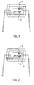
- FIG. 1 A cross-section of an optocoupler is shown in Figure 1.
- a light-emitting diode (LED) 10 generates light that impinges on the surface of a photodiode 20. If a transient electrical signal, such as a spike, appears at the input to the coupler, care must be taken to avoid transmission from the LED 10 to the photodiode 20.
- a transient electrical signal such as a spike
- an electric field may be generated at the LED 10. If the signal is large enough, the field will cross over to the photodiode 20, inducing a current in the photodiode 20.
- Such false indications can be avoided by placing a shield 30 to terminate the electric field between the LED 10 and the photodiode 20, as shown in Figure 2.
- the electrical shield 30 allows some portion of the light output of the LED 10 to pass through, but terminates the electrical field.
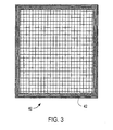
- the shield 30 can be fashioned as a grid of intersecting lines defining square, rectangular, triangular, or openings of other shapes.
- a grid 40 of square openings is shown in Figure 3.
- the shield 30 (or grid 40) could be deposited directly on the photodiode 20 as a layer having a thickness of 100 A to 20,000 A, depending on the process employed to fabricate the underlying devices. Alternatively, where the process provides a metallic interconnect layer, a portion of that layer can be utilized, isolating a section of the layer to create the shield 30 or grid 40.
- the lines used to create the shield 30 or grid 40 could be as wide (or narrow) as the photolithographic process allows, e.g., 0.2 ⁇ m, up to any desired width, and the spacing between the lines could be the same as the line width or greater to achieve a blockage of almost 90% or less.
- a spacing-to-line-width ratio of twenty-to-one, although other ratios, greater or lesser, could be chosen to suit the application.
- the shield 30 could be fashioned by depositing a series of parallel lines, concentric circles, or a spiral, again blocking the electrical field but allowing light to pass.
- the lines could be fabricated from any electrically-conductive material, such as aluminum, copper, gold, silver, polysilicon, and silicides.
- the shield 30 or grid 40 would be connected to a point at ground potential or another potential to help discharge any induced field. As shown in Figure 3, a border 42 at the periphery of the grid 40 provides a convenient connection point.
- the shield 30 may be employed in devices other than optocouplers, i.e., in any device where an electrical field requires termination.
Landscapes
- Photo Coupler, Interrupter, Optical-To-Optical Conversion Devices (AREA)
- Light Receiving Elements (AREA)
- Solid State Image Pick-Up Elements (AREA)
- Shielding Devices Or Components To Electric Or Magnetic Fields (AREA)
Abstract
Description
Claims (7)
- A shield for a semiconductor, comprising one or more electrically-conductive elements deposited over a portion of the surface of the semiconductor.
- A shield as set forth in claim 1, where the semiconductor is a photodiode.
- A shield as set forth in claim 1, where the elements define a grid.
- A shield as set forth in claim 1, where the elements define a series of parallel lines, concentric circles, or a spiral.
- A shield as set forth in claim 1, where the electrically-conductive elements are fabricated from a conductor such as aluminum, copper, gold, silver, polysilicon, or a silicide.
- A shield as set forth in claim 1, where the electrically-conductive elements are fabricated from an interconnect layer.
- A shield as set forth in claim 1, where the shield is connected to ground potential or another potential.
Applications Claiming Priority (2)
| Application Number | Priority Date | Filing Date | Title |
|---|---|---|---|
| US547475 | 2000-04-12 | ||
| US09/547,475 US6630623B1 (en) | 2000-04-12 | 2000-04-12 | Electrically-conductive grid shield for semiconductors |
Publications (2)
| Publication Number | Publication Date |
|---|---|
| EP1146568A2 true EP1146568A2 (en) | 2001-10-17 |
| EP1146568A3 EP1146568A3 (en) | 2003-10-08 |
Family
ID=24184778
Family Applications (1)
| Application Number | Title | Priority Date | Filing Date |
|---|---|---|---|
| EP01106679A Withdrawn EP1146568A3 (en) | 2000-04-12 | 2001-03-16 | Electrically-conductive grid shield for semiconductors |
Country Status (3)
| Country | Link |
|---|---|
| US (2) | US6630623B1 (en) |
| EP (1) | EP1146568A3 (en) |
| JP (1) | JP2002050732A (en) |
Families Citing this family (7)
| Publication number | Priority date | Publication date | Assignee | Title |
|---|---|---|---|---|
| FI117257B (en) * | 2003-12-15 | 2006-08-15 | Nokia Corp | Method and apparatus for protecting a component of electrostatic discharge |
| US20080125582A1 (en) * | 2006-10-13 | 2008-05-29 | Bio-Rad Laboratories, Inc. | Methods and compositions for stabilizing prostate specific antigen |
| TWI396499B (en) * | 2008-01-18 | 2013-05-11 | Asustek Comp Inc | Housing with shielding function and manufacturing method therefor and electronic device using the same |
| CN102024893B (en) * | 2010-05-29 | 2012-03-07 | 比亚迪股份有限公司 | Substrate, and LED chip with vertical structure and preparation method thereof |
| US8994117B2 (en) | 2012-12-18 | 2015-03-31 | International Business Machines Corporation | Moat construction to reduce noise coupling to a quiet supply |
| JP2016018832A (en) * | 2014-07-07 | 2016-02-01 | パナソニックIpマネジメント株式会社 | Optical coupling device |
| US11043479B2 (en) * | 2016-09-26 | 2021-06-22 | University Of New Hampshire | Opto-coupler with field-shaping end caps |
Family Cites Families (5)
| Publication number | Priority date | Publication date | Assignee | Title |
|---|---|---|---|---|
| JPS6018976A (en) * | 1983-07-13 | 1985-01-31 | Toshiba Corp | Semiconductor device |
| US5118924A (en) * | 1990-10-01 | 1992-06-02 | Eastman Kodak Company | Static control overlayers on opto-electronic devices |
| US5166772A (en) * | 1991-02-22 | 1992-11-24 | Motorola, Inc. | Transfer molded semiconductor device package with integral shield |
| US6184521B1 (en) * | 1998-01-06 | 2001-02-06 | Masimo Corporation | Photodiode detector with integrated noise shielding |
| US6169317B1 (en) * | 1998-02-13 | 2001-01-02 | Canon Kabushiki Kaisha | Photoelectric conversion device and image sensor |
-
2000
- 2000-04-12 US US09/547,475 patent/US6630623B1/en not_active Expired - Fee Related
-
2001
- 2001-03-16 EP EP01106679A patent/EP1146568A3/en not_active Withdrawn
- 2001-04-11 JP JP2001113229A patent/JP2002050732A/en active Pending
-
2003
- 2003-08-27 US US10/650,352 patent/US6787380B2/en not_active Expired - Fee Related
Also Published As
| Publication number | Publication date |
|---|---|
| US6787380B2 (en) | 2004-09-07 |
| JP2002050732A (en) | 2002-02-15 |
| US6630623B1 (en) | 2003-10-07 |
| US20040035598A1 (en) | 2004-02-26 |
| EP1146568A3 (en) | 2003-10-08 |
Similar Documents
| Publication | Publication Date | Title |
|---|---|---|
| DE112006002915B4 (en) | Integrated circuit and method for providing surge protection for low-voltage lines | |
| AU751678B2 (en) | Solar cell and process of manufacturing the same | |
| CA2196206A1 (en) | Semiconductor device with integrated rc network and schottky diode | |
| JP3786434B2 (en) | Integrated circuit | |
| JP2007005828A (en) | High-precision high-frequency capacitor formed on a semiconductor substrate | |
| DE102007061479A1 (en) | LED chip with surge protection | |
| US6630623B1 (en) | Electrically-conductive grid shield for semiconductors | |
| DE19612388C2 (en) | Integrated semiconductor circuit, in particular an optoelectronic component with overvoltage protection | |
| DE2839044A1 (en) | SEMICONDUCTOR DEVICE WITH SCHOTTKY BARRIER TRANSITION | |
| US4160992A (en) | Plural semiconductor devices mounted between plural heat sinks | |
| US20020134991A1 (en) | Semiconductor device for low voltage protection with low capacitance | |
| US6781161B1 (en) | Non-gated thyristor device | |
| Noyce | Semiconductor device-and-lead structure, reprint of us patent 2,981,877 (issued april 25, 1961. filed july 30, 1959) | |
| DE3345449A1 (en) | SOLID AC VOLTAGE RELAY | |
| CN102468109B (en) | Photomultiplier | |
| EP0335965A1 (en) | Phantom esd protection circuit employing e-field crowding | |
| JPH06268239A (en) | Surge absorbing diode | |
| JP2005167096A (en) | Semiconductor protection device | |
| EP0395862A3 (en) | Semiconductor device comprising a lead member | |
| JPH0541533A (en) | Semiconductor device | |
| JPS6159767A (en) | Semiconductor device | |
| JPH01289283A (en) | Photoelectric semiconductor element | |
| Mandy | Silicon planar epitaxial transistor | |
| JP2001244487A (en) | Photoelectric conversion element | |
| RO115474B1 (en) | Process for producing voltage limiter diodes |
Legal Events
| Date | Code | Title | Description |
|---|---|---|---|
| PUAI | Public reference made under article 153(3) epc to a published international application that has entered the european phase |
Free format text: ORIGINAL CODE: 0009012 |
|
| AK | Designated contracting states |
Kind code of ref document: A2 Designated state(s): AT BE CH CY DE DK ES FI FR GB GR IE IT LI LU MC NL PT SE TR |
|
| AX | Request for extension of the european patent |
Free format text: AL;LT;LV;MK;RO;SI |
|
| PUAL | Search report despatched |
Free format text: ORIGINAL CODE: 0009013 |
|
| AK | Designated contracting states |
Kind code of ref document: A3 Designated state(s): AT BE CH CY DE DK ES FI FR GB GR IE IT LI LU MC NL PT SE TR |
|
| AX | Request for extension of the european patent |
Extension state: AL LT LV MK RO SI |
|
| STAA | Information on the status of an ep patent application or granted ep patent |
Free format text: STATUS: THE APPLICATION IS DEEMED TO BE WITHDRAWN |
|
| 18D | Application deemed to be withdrawn |
Effective date: 20031001 |