EP1146538A2 - Plasma display panel - Google Patents
Plasma display panel Download PDFInfo
- Publication number
- EP1146538A2 EP1146538A2 EP00309828A EP00309828A EP1146538A2 EP 1146538 A2 EP1146538 A2 EP 1146538A2 EP 00309828 A EP00309828 A EP 00309828A EP 00309828 A EP00309828 A EP 00309828A EP 1146538 A2 EP1146538 A2 EP 1146538A2
- Authority
- EP
- European Patent Office
- Prior art keywords
- electrode
- display
- area
- column direction
- display panel
- Prior art date
- Legal status (The legal status is an assumption and is not a legal conclusion. Google has not performed a legal analysis and makes no representation as to the accuracy of the status listed.)
- Granted
Links
Images


Classifications
-
- H—ELECTRICITY
- H01—ELECTRIC ELEMENTS
- H01J—ELECTRIC DISCHARGE TUBES OR DISCHARGE LAMPS
- H01J11/00—Gas-filled discharge tubes with alternating current induction of the discharge, e.g. alternating current plasma display panels [AC-PDP]; Gas-filled discharge tubes without any main electrode inside the vessel; Gas-filled discharge tubes with at least one main electrode outside the vessel
- H01J11/20—Constructional details
- H01J11/22—Electrodes, e.g. special shape, material or configuration
- H01J11/24—Sustain electrodes or scan electrodes
-
- H—ELECTRICITY
- H01—ELECTRIC ELEMENTS
- H01J—ELECTRIC DISCHARGE TUBES OR DISCHARGE LAMPS
- H01J11/00—Gas-filled discharge tubes with alternating current induction of the discharge, e.g. alternating current plasma display panels [AC-PDP]; Gas-filled discharge tubes without any main electrode inside the vessel; Gas-filled discharge tubes with at least one main electrode outside the vessel
- H01J11/10—AC-PDPs with at least one main electrode being out of contact with the plasma
- H01J11/12—AC-PDPs with at least one main electrode being out of contact with the plasma with main electrodes provided on both sides of the discharge space
-
- H—ELECTRICITY
- H01—ELECTRIC ELEMENTS
- H01J—ELECTRIC DISCHARGE TUBES OR DISCHARGE LAMPS
- H01J11/00—Gas-filled discharge tubes with alternating current induction of the discharge, e.g. alternating current plasma display panels [AC-PDP]; Gas-filled discharge tubes without any main electrode inside the vessel; Gas-filled discharge tubes with at least one main electrode outside the vessel
- H01J11/20—Constructional details
- H01J11/22—Electrodes, e.g. special shape, material or configuration
- H01J11/26—Address electrodes
-
- H—ELECTRICITY
- H01—ELECTRIC ELEMENTS
- H01J—ELECTRIC DISCHARGE TUBES OR DISCHARGE LAMPS
- H01J11/00—Gas-filled discharge tubes with alternating current induction of the discharge, e.g. alternating current plasma display panels [AC-PDP]; Gas-filled discharge tubes without any main electrode inside the vessel; Gas-filled discharge tubes with at least one main electrode outside the vessel
- H01J11/20—Constructional details
- H01J11/34—Vessels, containers or parts thereof, e.g. substrates
- H01J11/36—Spacers, barriers, ribs, partitions or the like
-
- G—PHYSICS
- G09—EDUCATION; CRYPTOGRAPHY; DISPLAY; ADVERTISING; SEALS
- G09G—ARRANGEMENTS OR CIRCUITS FOR CONTROL OF INDICATING DEVICES USING STATIC MEANS TO PRESENT VARIABLE INFORMATION
- G09G2320/00—Control of display operating conditions
- G09G2320/02—Improving the quality of display appearance
- G09G2320/0209—Crosstalk reduction, i.e. to reduce direct or indirect influences of signals directed to a certain pixel of the displayed image on other pixels of said image, inclusive of influences affecting pixels in different frames or fields or sub-images which constitute a same image, e.g. left and right images of a stereoscopic display
-
- G—PHYSICS
- G09—EDUCATION; CRYPTOGRAPHY; DISPLAY; ADVERTISING; SEALS
- G09G—ARRANGEMENTS OR CIRCUITS FOR CONTROL OF INDICATING DEVICES USING STATIC MEANS TO PRESENT VARIABLE INFORMATION
- G09G2320/00—Control of display operating conditions
- G09G2320/02—Improving the quality of display appearance
- G09G2320/0247—Flicker reduction other than flicker reduction circuits used for single beam cathode-ray tubes
-
- G—PHYSICS
- G09—EDUCATION; CRYPTOGRAPHY; DISPLAY; ADVERTISING; SEALS
- G09G—ARRANGEMENTS OR CIRCUITS FOR CONTROL OF INDICATING DEVICES USING STATIC MEANS TO PRESENT VARIABLE INFORMATION
- G09G3/00—Control arrangements or circuits, of interest only in connection with visual indicators other than cathode-ray tubes
- G09G3/20—Control arrangements or circuits, of interest only in connection with visual indicators other than cathode-ray tubes for presentation of an assembly of a number of characters, e.g. a page, by composing the assembly by combination of individual elements arranged in a matrix no fixed position being assigned to or needed to be assigned to the individual characters or partial characters
- G09G3/22—Control arrangements or circuits, of interest only in connection with visual indicators other than cathode-ray tubes for presentation of an assembly of a number of characters, e.g. a page, by composing the assembly by combination of individual elements arranged in a matrix no fixed position being assigned to or needed to be assigned to the individual characters or partial characters using controlled light sources
- G09G3/28—Control arrangements or circuits, of interest only in connection with visual indicators other than cathode-ray tubes for presentation of an assembly of a number of characters, e.g. a page, by composing the assembly by combination of individual elements arranged in a matrix no fixed position being assigned to or needed to be assigned to the individual characters or partial characters using controlled light sources using luminous gas-discharge panels, e.g. plasma panels
- G09G3/288—Control arrangements or circuits, of interest only in connection with visual indicators other than cathode-ray tubes for presentation of an assembly of a number of characters, e.g. a page, by composing the assembly by combination of individual elements arranged in a matrix no fixed position being assigned to or needed to be assigned to the individual characters or partial characters using controlled light sources using luminous gas-discharge panels, e.g. plasma panels using AC panels
- G09G3/298—Control arrangements or circuits, of interest only in connection with visual indicators other than cathode-ray tubes for presentation of an assembly of a number of characters, e.g. a page, by composing the assembly by combination of individual elements arranged in a matrix no fixed position being assigned to or needed to be assigned to the individual characters or partial characters using controlled light sources using luminous gas-discharge panels, e.g. plasma panels using AC panels using surface discharge panels
-
- H—ELECTRICITY
- H01—ELECTRIC ELEMENTS
- H01J—ELECTRIC DISCHARGE TUBES OR DISCHARGE LAMPS
- H01J2211/00—Plasma display panels with alternate current induction of the discharge, e.g. AC-PDPs
- H01J2211/20—Constructional details
- H01J2211/22—Electrodes
- H01J2211/26—Address electrodes
- H01J2211/265—Shape, e.g. cross section or pattern
-
- H—ELECTRICITY
- H01—ELECTRIC ELEMENTS
- H01J—ELECTRIC DISCHARGE TUBES OR DISCHARGE LAMPS
- H01J2211/00—Plasma display panels with alternate current induction of the discharge, e.g. AC-PDPs
- H01J2211/20—Constructional details
- H01J2211/22—Electrodes
- H01J2211/32—Disposition of the electrodes
- H01J2211/323—Mutual disposition of electrodes
Definitions
- the present invention relates to a surface discharge type plasma display panel (PDP).
- PDP plasma display panel
- An AC surface discharge type PDP is commercialized as a display device of a television set having a large screen.
- the surface discharge type has first and second display electrodes that are anodes and cathodes in display discharge for ensuring a luminance and are arranged in parallel on a front or a back substrate.
- a "three-electrode structure" that has address electrodes arranged so as to cross display electrode pairs is well known as an electrode matrix structure of the surface discharge type PDP.
- One electrode of the display electrode pair (a second display electrode) is used as a scanning electrode for row selection, and the address discharge is generated between the scanning electrode and the address electrode so as to control wall charge for addressing in accordance with contents of display.
- a surface discharge occurs along a surface of a substrate only at cells having a predetermined quantity of the wall charge.
- a surface discharge type PDP is used in which N plus one display electrodes are arranged at a constant pitch in an interlaced display, where N is the number of rows of a screen.
- Fig. 11 is a plan view showing a cell structure of a conventional PDP.
- the display electrode Xz is a laminate of a banding transparent conductive film 41z extending linearly in the row direction and a metal film 42z having a small width for augmenting the conductivity.
- the metal film 42z is arranged at the middle of the transparent conductive film 41z in the column direction.
- the display electrode Yz includes a transparent conductive film 41z and a metal film 42z.
- a total of N+1 display electrodes Xz and Yz are arranged alternately, and the neighboring display electrodes Xz and Yz make an electrode pair for generating surface discharge, so as to form a row of screen.
- Each of the display electrodes Xz, Yz except both ends of the arrangement relates to display of two rows (an odd row and an even row), while the display electrodes Xz, Yz at the both ends relate to display of one row.
- a discharge space is divided in each column by partitions 29z, and one column space that is a discharge space of one column is continuous over all rows.
- a structure of an area defined by neighboring partitions 29z and neighboring metal films 42z is a discharge cell (a display element) Cz.
- the address electrode Az is arranged at the middle of the column space.
- An example of a driving method is as follows. In both address periods of an odd field and an even field, a scan pulse is applied to each display electrode Yz sequentially. Then, a potential of the odd display electrode Xz and a potential of the even display electrode Xz are switched complementarily at each application of the scan pulse, so that an address discharge is generated between the display electrodes at the row for display (e.g., at an odd row in an odd field).
- a sustaining pulse is applied alternately to the display electrodes Xz and Yz of the row that are used for the display, and a sustaining pulse is applied to the display electrode Xz of the row that is not used for the display (e.g., an even row in an odd field) in the same timing as the display electrode Yz.
- a sustaining pulse is applied to the display electrode Xz of the row that is not used for the display (e.g., an even row in an odd field) in the same timing as the display electrode Yz.
- the discharge gas space is divided in units of two cells aligned in the column direction.
- a scanning electrode that is one electrode of the display electrode pair is not used, but the other display electrode is used for dividing in the column direction. Since the dividing unit has an area of two cells, the light emission area of the odd row can overlap the light emission area of the even row in the column direction, so that the flicker is less conspicuous. Even if a cross talk of the discharge occurs, the fluctuation of the display is little since the cross talk is limited to the area of two cells or the multiples of the area. Since the discharge between the scanning electrode and the address electrode is not disturbed by the partition, a stable addressing can b e performed.
- a plasma display panel comprises plural sets of first and second display electrodes making an electrode pair for surface discharge of each row, being arranged so that one electrode is shared by two neighboring rows for display, plural address electrodes crossing the electrode pair in each column, the second display electrode being a scanning electrode for row selection, and one or more partitions for dividing a discharge gas space in the column direction and only in a position within the area where the first display electrode is arranged.
- the address electrode has a first area opposite the first display electrode and a second area opposite the second display electrode, and the second area is larger than the first area.
- each of the first and the second display electrodes includes a transparent conductive film for ensuring an electrode area and a metal film for reducing a resistance
- the address electrode has a first area opposite the metal film of the first display electrode and a second area opposite the metal film of the second display electrode, the second area being larger than the first area
- the portion of the partition that divides the discharge gas space in the column direction is arranged at the middle of the first display electrode in the column direction.
- the shape of the first display electrode is different from the shape of the second display electrode so that discharge characteristics of cells are made uniform.
- the portion of the partition that divides the discharge gas space in the column direction is formed so as to have a gap that makes the discharge gas space continuous in the column direction.
- the first display electrode includes plural conductors separated from each other in the column direction within a screen area.
- each of the first and the second display electrode includes a transparent conductive film for ensuring an electrode area and a metal film for reducing a resistance, and the portion of the partition that divides the discharge gas space in the column direction is formed so as to overlap the metal film of the first display electrode.
- the PDP has three kinds of cells corresponding to three kinds of light emission colors, and an effective area of at least one of the first and the second display electrodes is adjusted for each light emission color, so that relative luminance of the each color can be adjusted.
- Fig. 1 shows a cell structure of a plasma display panel (PDP) according to a first embodiment of the present invention.
- Fig. 2 is a plan view showing a partition pattern of the PDP according to the first embodiment.
- the illustrated PDP 1 has a pair of substrate structures (including cell constructing elements on a substrate) 10, 20, and has a three-electrode surface discharge structure.
- a pair of display electrodes X, Y and an address electrode A cross each other.
- the display electrodes X, Y are arranged on the inner surface of a glass substrate 11 of a front substrate structure 10.
- Each of the display electrodes X, Y has a transparent conductive film 41 that forms a surface discharge gap for each cell and a metal film (a bus conductor) 42 that is overlaid on the middle of the conductive film 41 in the column direction.
- the metal film 42 is drawn out of the screen ES, so as to connect with a drive circuit.
- the display electrodes X, Y are covered with a dielectric layer 17 having a thickness of approximately 30-50 ⁇ m, and the dielectric layer 17 is coated with magnesia (MgO) as a protection film 18.
- MgO magnesia
- the address electrodes A are arranged on the inner surface of a glass substrate 21 of a back substrate structure 20, and are covered with a dielectric layer 24.
- partitions 29 having a height of approximately 150 ⁇ m for defining a discharge gas space 31 of two cells are provided in the present invention.
- the partition 29 includes a portion for dividing the discharge gas space into columns (hereinafter, referred to as a vertical portion) 291 and a portion for dividing the discharge gas space at an appropriate position in the column direction (hereinafter, referred to as a horizontal portion) 292.
- Three colors of fluorescent layers 28R, 28G and 28B for color display are arranged to as to cover the inner surface of the back side including the surface of the dielectric layer covering the address electrode A and the side face of the partition 29.
- the fluorescent layers 28R, 28G and 28B are excited locally by ultraviolet rays emitted by a discharge gas and emit light. Italic characters (R, G and B) in Fig. 1 indicate light emission colors of the fluorescent materials.
- a horizontal portion 292 of the partition 29 is formed only at the position of the display electrode X of the display electrodes X, Y that are arranged alternately so as to ensure the reliability of addressing.
- the display electrode X is an electrode that is not used for row selection.
- the division of the discharge gas space is not performed at the position of the display electrode Y that is used as a scanning electrode.
- a vertical portion 291 of the partition 29 is arranged as a boundary wall between columns, and the partition pattern is a mesh pattern surrounding two cells C of rows in each column. Even if the discharge overspreads in a cell C excessively, the cross talk is localized in the discharge gas space 31 of two cells. In addition, discharge areas (light emission areas having a predetermined intensity) Eul, Eu2 of two cells C sharing discharge gas space 31 overlap each other. Thus, when two cells C are lighted alternately every field in an interlace display of two to one, the quality of display becomes close to that when one cell C is lighted continuously over plural fields. Namely, a flicker is not conspicuous. If the division by the unit of two cells is difficult in a practical micro machining technology (e.g. in a high-definition panel with micro cells), the discharge gas space can be divided by a unit of 2m cells such as four cells or six cells.
- FIGs. 3A and 3B are perspective views showing a variation of the three-dimensional structure of the partition.
- each element corresponding to that of the above-mentioned example is denoted by the same reference numerals as in Figs. 1 and 2. The same applies to the subsequent figures.
- the partition 29b shown in Fig. 3A has a height h2 of the horizontal portion 293 parallel to the row direction lower than the height h1 of the vertical portion 291 parallel to the column direction. This height difference makes the discharge gas space communicate from one end to the other end in each column, so that the time necessary for exhausting air and injecting a gas can be shortened in the assembling step of the PDP 1.
- An appropriate height h2 enables the horizontal portion 293 to suppress the cross talk sufficiently.
- the discharge gas space is divided by plural partitions 29c that are arranged in the row direction with a slit 33.
- Each partition 29c includes the above-mentioned vertical portion 291 and a horizontal portion 294 extending from the vertical portion 291 in the row direction.
- the set of partitions 29c corresponds to the structure in which the portion 292 is cut off out of the partition 29 at the middle of the column as shown in Fig. 2.
- the slit 33 makes the discharge gas space communicate in each column.
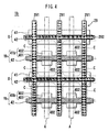
- Fig. 4 is a plan view showing a first variation of the display electrode shape.
- a PDP 1b in Fig. 4 has a display electrode Yb that is used for a scanning electrode, which includes a transparent conductive film 41b of a tooth-like shape extending over the entire length of the row and a linear banding metal film 42.
- the transparent conductive film 41b includes a protruding portion 402 defining a discharge portion of each column and a base portion 401 connecting the protruding portions 402.
- This structure can equalize the effective electrode areas of the display electrode X and the display electrode Yb by setting the size of the protruding portion 402. If the electrode areas are equal, the display discharge with the display electrode X as an anode has the same discharge condition as the display discharge with the display electrode Yb as an anode, so that more stable display can be realized.
- the display electrode Yb for scanning can have a structure in which the transparent conductive film is made in the shape of plural straps separated in each column, and these strap conductive films are connected by the linear banding metal film 42.
- Fig. 5 is a plan view showing a second variation of the display electrode shape.
- the width of the display electrode Yc that is used as a scanning electrode i.e., the width of the transparent conductive film 41c
- the width Wx of the display electrode X at the portion of one row display are selected so that the effective electrode areas of the display electrodes X, Yc becomes equal.
- Fig. 6 is a plan view showing an electrode structure of a PDP according to a second embodiment of the present invention.
- the PDP 2 of Fig. 6 has address electrodes Ad, each of which is patterned in such a banding shape that a portion crossing the display electrode Yd is thicker than other portions so as to ensure a larger margin of the addressing voltage. Enlarging the opposing area between the display electrode Yd and the address electrode Ad can increase the probability of addressing discharge, so that the address discharge can be generated easily. In contrast, it is desirable that the opposing area between the display electrode X and the address electrode Ad is as small as possible for reducing a capacitance.
- the display electrode Yd includes a transparent conductive film 41d of a tooth-like shape extending over the entire length of the row and a linear banding metal film 42.
- the transparent conductive film 41d includes a linear banding base portion 401 and a protruding portion 403 that defines a discharge portion of each column. Each protruding portion 403 is patterned to extend from the base portion 401 in T-shape.
- the illustrated shape of the transparent conductive film 41d is effective for reducing a discharge current and for suppressing a cross talk.
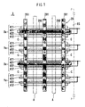
- Fig. 7 is a plan view showing an electrode structure of a PDP according to a third embodiment of the present invention.
- the PDP 3 has display electrodes Xe, Ye made of a pair of conductors separated in the column direction.
- One of the conductors includes a transparent conductive film 411 and a metal film 421.
- the other conductor includes a transparent conductive film 412 and a metal film 422.
- the metal film 421 and the metal film 422 are connected to each other in the outside of the screen ES and can be regarded as a unit of conductor.
- the display electrode Ye is divided in the column direction so that the two cells C that are surrounded by the partition 29 generate hardly any cross talk.
- the display electrode Xe is divided in the column direction so that the portion of the partition 29 that is surrounded by the horizontal portion 292 and does not contribute the discharge does not have the display electrode Xe.
- the opposing area between the display electrode Xe and the address electrode A is decreased by the gap so that the capacitance can decrease.
- the portion that does not contribute to the discharge is sandwiched by a pair of conductors that constitute the display electrode Xe and is a part of the area in which the display electrode Xe is positioned.
- the area in which the display electrode is positioned means an area from one end to the other end of the display electrode in the column direction.
- Fig. 8 is a plan view showing an electrode structure of a PDP according to a fourth embodiment of the present invention.
- the display electrode Xe of the display electrodes Xe, Yc is divided into two in the column direction, and the size of the display electrode Yc is the same as the example shown in Fig. 5.
- the discharge gas space is divided with the partition 29c explained with reference to Fig. 3B.
- a slit 33 that enhances air permeability in the column direction also makes a cross talk liable to occur over the display electrode Xe.
- the display electrode Xe is divided, and an electrode gap is provided between rows, so that the cross talk can be localized in the area of two cells and the air permeability can be enhanced.
- Fig. 9 is a plan view showing a variation of the electrode structure of the PDP in the fourth embodiment.
- the display electrode Xf includes a pair of transparent conductive films 411, 412 that are separated in the column direction and a ladder-like metal film 423.
- the metal film 423 includes a portion 423A corresponding to a pair of metal films 421, 422 shown in Fig. 8 and a portion 423B that connects the portion 423A at the position overlapping the partition 29c.
- the portion 423B decreases the probability of destroying the function of the metal film 423 due to a break at the portion 423A. The discharge cannot spread along the portion 423B that is overlapped by the partition 29c.
- the address electrode Af is patterned in such a banding shape that a portion crossing the display electrode Y that includes the metal film 42 and the transparent conductive film 41 is thick.
- the opposing area between the display electrode Y and the address electrode Af is larger than the opposing area between the display electrode Xf and the address electrode Af.
- Fig. 10 is a plan view showing an electrode structure of a PDP according to a fifth embodiment of the present invention.
- the display electrode Yg includes a transparent conductive film 41g having a tooth-like pattern extending over the entire length of the row and a linear banding metal film 42.
- the transparent conductive film 41g includes a linear banding base portion 401 and protruding portions 405, 406, 407 defining the discharge portion in each column.
- Each of the protruding portions 405, 406, 407 is patterned to extend from the base portion 401 in T-shape.
- the areas of protruding portions 405, 406, 407 are optimized in accordance with the light emission color of the corresponding column, so that the white balance of the color display can be optimized.
- the width Wr of the protruding portion 405 in the column whose light emission color is red, the width Wg of the protruding portion 406 in the column whose light emission color is green, and the width Wb of the protruding portion 407 in the column whose light emission color is blue have the relationship of Wr ⁇ Wg ⁇ Wb.
- the present invention can be embodied by combining the examples concerning the partition pattern, the display electrode shape and the address electrode shape without being limited to the above-mentioned examples.
- the display electrode can be a metal electrode having a mesh shape instead of using the transparent conductive film.
- the reliability of addressing can be ensured and the flicker can be reduced.
- the area where cross talk can spread in the column direction can be decreased so that a fluctuation of the display can be reduced.
- the margin of the addressing voltage can be enlarged.
Landscapes
- Engineering & Computer Science (AREA)
- Physics & Mathematics (AREA)
- Plasma & Fusion (AREA)
- Chemical & Material Sciences (AREA)
- Materials Engineering (AREA)
- Gas-Filled Discharge Tubes (AREA)
Abstract
Description
- The present invention relates to a surface discharge type plasma display panel (PDP).
- An AC surface discharge type PDP is commercialized as a display device of a television set having a large screen. The surface discharge type has first and second display electrodes that are anodes and cathodes in display discharge for ensuring a luminance and are arranged in parallel on a front or a back substrate.
- A "three-electrode structure" that has address electrodes arranged so as to cross display electrode pairs is well known as an electrode matrix structure of the surface discharge type PDP. One electrode of the display electrode pair (a second display electrode) is used as a scanning electrode for row selection, and the address discharge is generated between the scanning electrode and the address electrode so as to control wall charge for addressing in accordance with contents of display. After the addressing, by applying a sustaining voltage having alternating polarity to the display electrode pair, a surface discharge occurs along a surface of a substrate only at cells having a predetermined quantity of the wall charge.
- Conventionally, a surface discharge type PDP is used in which N plus one display electrodes are arranged at a constant pitch in an interlaced display, where N is the number of rows of a screen.
- Fig. 11 is a plan view showing a cell structure of a conventional PDP.
- The display electrode Xz is a laminate of a banding transparent
conductive film 41z extending linearly in the row direction and ametal film 42z having a small width for augmenting the conductivity. Themetal film 42z is arranged at the middle of the transparentconductive film 41z in the column direction. In the same way, the display electrode Yz includes a transparentconductive film 41z and ametal film 42z. A total of N+1 display electrodes Xz and Yz are arranged alternately, and the neighboring display electrodes Xz and Yz make an electrode pair for generating surface discharge, so as to form a row of screen. Each of the display electrodes Xz, Yz except both ends of the arrangement relates to display of two rows (an odd row and an even row), while the display electrodes Xz, Yz at the both ends relate to display of one row. - A discharge space is divided in each column by
partitions 29z, and one column space that is a discharge space of one column is continuous over all rows. A structure of an area defined by neighboringpartitions 29z and neighboringmetal films 42z is a discharge cell (a display element) Cz. The address electrode Az is arranged at the middle of the column space. - An example of a driving method is as follows. In both address periods of an odd field and an even field, a scan pulse is applied to each display electrode Yz sequentially. Then, a potential of the odd display electrode Xz and a potential of the even display electrode Xz are switched complementarily at each application of the scan pulse, so that an address discharge is generated between the display electrodes at the row for display (e.g., at an odd row in an odd field). In the display period following the address period, a sustaining pulse is applied alternately to the display electrodes Xz and Yz of the row that are used for the display, and a sustaining pulse is applied to the display electrode Xz of the row that is not used for the display (e.g., an even row in an odd field) in the same timing as the display electrode Yz. Namely, potential changes in the pair of display electrodes in the row that are not used for the display are in phase. Thus, discharge interference between an odd row and an even row can be reduced.
- There is a problem of the conventional PDP in that since the column space is continuous over the entire length of the screen in the column direction, a cross talk of discharge can be generated in wide area over a few rows or a few tens of rows. In the structure having display electrodes arranged at a constant pitch, a displaying row and a non-displaying row are determined only by controlling their electrode potential. Therefore, the cross talk can occur easily compared with the structure in which a pair of display electrodes is arranged for each row so that an electrode gap between rows can be sufficiently wide. In order to eliminate the cross talk, a mesh pattern or a waffle pattern of partition can be provided for separating the cells, but this reduces the electrode area contributing to the discharge, resulting in reduction of display luminance. Since a main portion of the scanning electrode (Yz) is covered with the partition, an addressing potential may rise and a delay of discharge may occur. In addition, since an interlaced display uses odd rows and even rows in time sharing for light emission, the separation of the cell will cause non-overlap of light emission areas of the odd row and the even row, resulting in a conspicuous flicker due to the time sharing light emission.
- Accordingly, it is desirable to ensure a reliability of addressing, to reduce flicker and to decrease the area of cross talk in the column direction so that a display fluctuation can be reduced.
- According to the present invention, the discharge gas space is divided in units of two cells aligned in the column direction. A scanning electrode that is one electrode of the display electrode pair is not used, but the other display electrode is used for dividing in the column direction. Since the dividing unit has an area of two cells, the light emission area of the odd row can overlap the light emission area of the even row in the column direction, so that the flicker is less conspicuous. Even if a cross talk of the discharge occurs, the fluctuation of the display is little since the cross talk is limited to the area of two cells or the multiples of the area. Since the discharge between the scanning electrode and the address electrode is not disturbed by the partition, a stable addressing can b e performed.
- According to the present invention, a plasma display panel (PDP) comprises plural sets of first and second display electrodes making an electrode pair for surface discharge of each row, being arranged so that one electrode is shared by two neighboring rows for display, plural address electrodes crossing the electrode pair in each column, the second display electrode being a scanning electrode for row selection, and one or more partitions for dividing a discharge gas space in the column direction and only in a position within the area where the first display electrode is arranged.
- Preferably, the address electrode has a first area opposite the first display electrode and a second area opposite the second display electrode, and the second area is larger than the first area.
- Preferably also, each of the first and the second display electrodes includes a transparent conductive film for ensuring an electrode area and a metal film for reducing a resistance, and the address electrode has a first area opposite the metal film of the first display electrode and a second area opposite the metal film of the second display electrode, the second area being larger than the first area.
- In an embodiment of the present invention, the portion of the partition that divides the discharge gas space in the column direction is arranged at the middle of the first display electrode in the column direction.
- In another embodiment of the present invention, the shape of the first display electrode is different from the shape of the second display electrode so that discharge characteristics of cells are made uniform.
- It is possible to make an effective area of the first display electrode different from an effective area of the second display electrode so that discharge characteristics of cells are made uniform.
- In a further embodiment, the portion of the partition that divides the discharge gas space in the column direction is formed so as to have a gap that makes the discharge gas space continuous in the column direction.
- In another preferred arrangement, the first display electrode includes plural conductors separated from each other in the column direction within a screen area.
- In a further embodiment of the invention, each of the first and the second display electrode includes a transparent conductive film for ensuring an electrode area and a metal film for reducing a resistance, and the portion of the partition that divides the discharge gas space in the column direction is formed so as to overlap the metal film of the first display electrode.
- Moreover, it is preferred that the PDP has three kinds of cells corresponding to three kinds of light emission colors, and an effective area of at least one of the first and the second display electrodes is adjusted for each light emission color, so that relative luminance of the each color can be adjusted.
- Reference will now be made, by way of example only, to the accompanying drawings in which:-
- Fig. 1 shows a cell structure of a PDP according to a first embodiment of the present invention. .
- Fig. 2 is a plan view showing a partition pattern of the PDP according to the first embodiment.
- Figs. 3A and 3B are perspective views showing a variation of the three-dimensional structure of the partition.
- Fig. 4 is a plan view showing a first variation of the display electrode shape.
- Fig. 5 is a plan view showing a second variation of the display electrode shape.
- Fig. 6 is a plan view showing an electrode structure of a PDP according to the a embodiment of the present invention.
- Fig. 7 is a plan view showing an electrode structure of a PDP according to a third embodiment of the present invention.
- Fig. 8 is a plan view showing an electrode structure of a PDP according to a fourth embodiment of the present invention.
- Fig. 9 is a plan view showing a variation of the electrode structure of the PDP in the fourth embodiment.
- Fig. 10 is a plan view showing an electrode structure of a PDP according to a fifth embodiment of the present invention.
- Fig. 11 is a plan view showing a cell structure of a conventional PDP.
-
- Hereinafter, the present invention will be explained in detail with reference to embodiments thereof.
- Fig. 1 shows a cell structure of a plasma display panel (PDP) according to a first embodiment of the present invention. Fig. 2 is a plan view showing a partition pattern of the PDP according to the first embodiment.
- The illustrated
PDP 1 has a pair of substrate structures (including cell constructing elements on a substrate) 10, 20, and has a three-electrode surface discharge structure. In each cell of a screen (a display surface) ES, a pair of display electrodes X, Y and an address electrode A cross each other. The display electrodes X, Y are arranged on the inner surface of aglass substrate 11 of afront substrate structure 10. Each of the display electrodes X, Y has a transparentconductive film 41 that forms a surface discharge gap for each cell and a metal film (a bus conductor) 42 that is overlaid on the middle of theconductive film 41 in the column direction. Themetal film 42 is drawn out of the screen ES, so as to connect with a drive circuit. The display electrodes X, Y are covered with adielectric layer 17 having a thickness of approximately 30-50 µm, and thedielectric layer 17 is coated with magnesia (MgO) as aprotection film 18. - The address electrodes A are arranged on the inner surface of a
glass substrate 21 of aback substrate structure 20, and are covered with adielectric layer 24. On thedielectric layer 24,partitions 29 having a height of approximately 150 µm for defining adischarge gas space 31 of two cells are provided in the present invention. Thepartition 29 includes a portion for dividing the discharge gas space into columns (hereinafter, referred to as a vertical portion) 291 and a portion for dividing the discharge gas space at an appropriate position in the column direction (hereinafter, referred to as a horizontal portion) 292. Three colors offluorescent layers partition 29. The fluorescent layers 28R, 28G and 28B are excited locally by ultraviolet rays emitted by a discharge gas and emit light. Italic characters (R, G and B) in Fig. 1 indicate light emission colors of the fluorescent materials. - As shown in Fig. 2, a
horizontal portion 292 of thepartition 29 is formed only at the position of the display electrode X of the display electrodes X, Y that are arranged alternately so as to ensure the reliability of addressing. The display electrode X is an electrode that is not used for row selection. The division of the discharge gas space is not performed at the position of the display electrode Y that is used as a scanning electrode. - A
vertical portion 291 of thepartition 29 is arranged as a boundary wall between columns, and the partition pattern is a mesh pattern surrounding two cells C of rows in each column. Even if the discharge overspreads in a cell C excessively, the cross talk is localized in thedischarge gas space 31 of two cells. In addition, discharge areas (light emission areas having a predetermined intensity) Eul, Eu2 of two cells C sharingdischarge gas space 31 overlap each other. Thus, when two cells C are lighted alternately every field in an interlace display of two to one, the quality of display becomes close to that when one cell C is lighted continuously over plural fields. Namely, a flicker is not conspicuous. If the division by the unit of two cells is difficult in a practical micro machining technology (e.g. in a high-definition panel with micro cells), the discharge gas space can be divided by a unit of 2m cells such as four cells or six cells. - Figs. 3A and 3B are perspective views showing a variation of the three-dimensional structure of the partition. In Figs. 3A and 3B, each element corresponding to that of the above-mentioned example is denoted by the same reference numerals as in Figs. 1 and 2. The same applies to the subsequent figures.
- The
partition 29b shown in Fig. 3A has a height h2 of thehorizontal portion 293 parallel to the row direction lower than the height h1 of thevertical portion 291 parallel to the column direction. This height difference makes the discharge gas space communicate from one end to the other end in each column, so that the time necessary for exhausting air and injecting a gas can be shortened in the assembling step of thePDP 1. An appropriate height h2 enables thehorizontal portion 293 to suppress the cross talk sufficiently. - In the example of Fig. 3B, the discharge gas space is divided by
plural partitions 29c that are arranged in the row direction with aslit 33. Eachpartition 29c includes the above-mentionedvertical portion 291 and ahorizontal portion 294 extending from thevertical portion 291 in the row direction. The set ofpartitions 29c corresponds to the structure in which theportion 292 is cut off out of thepartition 29 at the middle of the column as shown in Fig. 2. Theslit 33 makes the discharge gas space communicate in each column. - Fig. 4 is a plan view showing a first variation of the display electrode shape.
- A
PDP 1b in Fig. 4 has a display electrode Yb that is used for a scanning electrode, which includes a transparentconductive film 41b of a tooth-like shape extending over the entire length of the row and a linearbanding metal film 42. The transparentconductive film 41b includes a protrudingportion 402 defining a discharge portion of each column and abase portion 401 connecting the protrudingportions 402. This structure can equalize the effective electrode areas of the display electrode X and the display electrode Yb by setting the size of the protrudingportion 402. If the electrode areas are equal, the display discharge with the display electrode X as an anode has the same discharge condition as the display discharge with the display electrode Yb as an anode, so that more stable display can be realized. In addition, since the banding display electrode Yb is thick at the middle of each column and is thin at both ends, an average distance between the display electrode X and the display electrode Yb becomes larger than the case of a constant width of the banding shape, so that a capacitance between the electrodes is reduced. The display electrode Yb for scanning can have a structure in which the transparent conductive film is made in the shape of plural straps separated in each column, and these strap conductive films are connected by the linearbanding metal film 42. - Fig. 5 is a plan view showing a second variation of the display electrode shape.
- In a
PDP 1c of Fig. 5, the width of the display electrode Yc that is used as a scanning electrode (i.e., the width of the transparentconductive film 41c) Wy and the width Wx of the display electrode X at the portion of one row display are selected so that the effective electrode areas of the display electrodes X, Yc becomes equal. - Fig. 6 is a plan view showing an electrode structure of a PDP according to a second embodiment of the present invention.
- The
PDP 2 of Fig. 6 has address electrodes Ad, each of which is patterned in such a banding shape that a portion crossing the display electrode Yd is thicker than other portions so as to ensure a larger margin of the addressing voltage. Enlarging the opposing area between the display electrode Yd and the address electrode Ad can increase the probability of addressing discharge, so that the address discharge can be generated easily. In contrast, it is desirable that the opposing area between the display electrode X and the address electrode Ad is as small as possible for reducing a capacitance. - The display electrode Yd includes a transparent
conductive film 41d of a tooth-like shape extending over the entire length of the row and a linearbanding metal film 42. The transparentconductive film 41d includes a linearbanding base portion 401 and a protrudingportion 403 that defines a discharge portion of each column. Each protrudingportion 403 is patterned to extend from thebase portion 401 in T-shape. The illustrated shape of the transparentconductive film 41d is effective for reducing a discharge current and for suppressing a cross talk. - Fig. 7 is a plan view showing an electrode structure of a PDP according to a third embodiment of the present invention.
- The
PDP 3 has display electrodes Xe, Ye made of a pair of conductors separated in the column direction. One of the conductors includes a transparentconductive film 411 and ametal film 421. The other conductor includes a transparentconductive film 412 and ametal film 422. In each of the display electrodes Xe, Ye, themetal film 421 and themetal film 422 are connected to each other in the outside of the screen ES and can be regarded as a unit of conductor. - The display electrode Ye is divided in the column direction so that the two cells C that are surrounded by the
partition 29 generate hardly any cross talk. In addition, the display electrode Xe is divided in the column direction so that the portion of thepartition 29 that is surrounded by thehorizontal portion 292 and does not contribute the discharge does not have the display electrode Xe. The opposing area between the display electrode Xe and the address electrode A is decreased by the gap so that the capacitance can decrease. However, the portion that does not contribute to the discharge is sandwiched by a pair of conductors that constitute the display electrode Xe and is a part of the area in which the display electrode Xe is positioned. Namely, the area in which the display electrode is positioned means an area from one end to the other end of the display electrode in the column direction. - Fig. 8 is a plan view showing an electrode structure of a PDP according to a fourth embodiment of the present invention.
- In the PDP 4, the display electrode Xe of the display electrodes Xe, Yc is divided into two in the column direction, and the size of the display electrode Yc is the same as the example shown in Fig. 5. The discharge gas space is divided with the
partition 29c explained with reference to Fig. 3B. A slit 33 that enhances air permeability in the column direction also makes a cross talk liable to occur over the display electrode Xe. In PDP 4, the display electrode Xe is divided, and an electrode gap is provided between rows, so that the cross talk can be localized in the area of two cells and the air permeability can be enhanced. - Fig. 9 is a plan view showing a variation of the electrode structure of the PDP in the fourth embodiment.
- In the
PDP 4b, the display electrode Xf includes a pair of transparentconductive films like metal film 423. Themetal film 423 includes aportion 423A corresponding to a pair ofmetal films portion 423B that connects theportion 423A at the position overlapping thepartition 29c. Theportion 423B decreases the probability of destroying the function of themetal film 423 due to a break at theportion 423A. The discharge cannot spread along theportion 423B that is overlapped by thepartition 29c. - In the
PDP 4b, the address electrode Af is patterned in such a banding shape that a portion crossing the display electrode Y that includes themetal film 42 and the transparentconductive film 41 is thick. The opposing area between the display electrode Y and the address electrode Af is larger than the opposing area between the display electrode Xf and the address electrode Af. - Fig. 10 is a plan view showing an electrode structure of a PDP according to a fifth embodiment of the present invention.
- In the
PDP 5 of Fig. 10, the display electrode Yg includes a transparentconductive film 41g having a tooth-like pattern extending over the entire length of the row and a linearbanding metal film 42. The transparentconductive film 41g includes a linearbanding base portion 401 and protrudingportions portions base portion 401 in T-shape. However, differently from the example of Fig. 6, the areas of protrudingportions portion 405 in the column whose light emission color is red, the width Wg of the protrudingportion 406 in the column whose light emission color is green, and the width Wb of the protrudingportion 407 in the column whose light emission color is blue have the relationship of Wr < Wg < Wb. - The present invention can be embodied by combining the examples concerning the partition pattern, the display electrode shape and the address electrode shape without being limited to the above-mentioned examples. In addition, the display electrode can be a metal electrode having a mesh shape instead of using the transparent conductive film.
- According to the present invention, the reliability of addressing can be ensured and the flicker can be reduced. In addition, the area where cross talk can spread in the column direction can be decreased so that a fluctuation of the display can be reduced.
- According to another feature of the present invention, the margin of the addressing voltage can be enlarged.
- While the presently preferred embodiments of the present invention have been shown and described, it will be understood that the present invention is not limited thereto, and that various changes and modifications may be made by those skilled in the art without departing from the scope of the invention as set forth in the appended claims.
Claims (10)
- A plasma display panel comprising:plural sets of first and second display electrodes making an electrode pair for surface discharge of each row, being arranged so that one electrode is shared by two neighboring rows for display;plural address electrodes crossing the electrode pair in each column;the second display electrode being a scanning electrode for row selection; andone or more partitions for dividing a discharge gas space in the column direction and only in a position within the area where the first display electrode is arranged.
- The plasma display panel according to claim 1, wherein the address electrode has a first area opposite the first display electrode and a second area opposite the second display electrode, and the second area is larger than the first area.
- The plasma display panel according to claim 1, wherein each of the first and the second display electrodes includes a transparent conductive film for ensuring an electrode area and a metal film for reducing a resistance, and the address electrode has a first area opposite the metal film of the first display electrode and a second area opposite the metal film of the second display electrode, the second area being larger than the first area.
- The plasma display panel according to claim 1, 2, or 3, wherein the portion of the partition that divides the discharge gas space in the column direction is arranged at the middle of the first display electrode in the column direction.
- The plasma display panel according to claim 1, 2, 3, or 4, wherein the shape of the first display electrode is different from the shape of the second display electrode so that discharge characteristics of cells are made uniform.
- The plasma display panel according to any preceding claim, wherein an effective area of the first display electrode is different from an effective area of the second display electrode so that discharge characteristics of cells are made uniform.
- The plasma display panel according to any preceding claim, wherein the portion of the partition that divides the discharge gas space in the column direction is formed so as to have a gap that makes the discharge gas space continuous in the column direction.
- The plasma display panel according to any preceding claim, wherein the first display electrode includes plural conductors separated from each other in the column direction within a screen area.
- The plasma display panel according to claim 1 or 2, wherein each of the first and the second display electrodes includes a transparent conductive film for ensuring an electrode area and a metal film for reducing a resistance, and the portion of the partition that divides the discharge gas space in the column direction is formed so as to overlap the metal film of the first display electrode.
- The plasma display panel according to any preceding claim, having three kinds of cells corresponding to three kinds of light emission colors, wherein an effective area of at least one of the first and the second display electrodes is adjusted for each light emission color, so that reflective luminance of the each color can be adjusted.
Applications Claiming Priority (2)
| Application Number | Priority Date | Filing Date | Title |
|---|---|---|---|
| JP2000079428A JP2001266750A (en) | 2000-03-22 | 2000-03-22 | Plasma display panel |
| JP2000079428 | 2000-03-22 |
Publications (3)
| Publication Number | Publication Date |
|---|---|
| EP1146538A2 true EP1146538A2 (en) | 2001-10-17 |
| EP1146538A3 EP1146538A3 (en) | 2004-03-31 |
| EP1146538B1 EP1146538B1 (en) | 2008-07-23 |
Family
ID=18596678
Family Applications (1)
| Application Number | Title | Priority Date | Filing Date |
|---|---|---|---|
| EP00309828A Expired - Lifetime EP1146538B1 (en) | 2000-03-22 | 2000-11-06 | Plasma display panel |
Country Status (6)
| Country | Link |
|---|---|
| US (1) | US6489722B1 (en) |
| EP (1) | EP1146538B1 (en) |
| JP (1) | JP2001266750A (en) |
| KR (1) | KR100730325B1 (en) |
| DE (1) | DE60039581D1 (en) |
| TW (1) | TW498381B (en) |
Cited By (4)
| Publication number | Priority date | Publication date | Assignee | Title |
|---|---|---|---|---|
| EP1271599A2 (en) | 2001-06-29 | 2003-01-02 | Pioneer Corporation | Plasma display panel |
| EP1646065A2 (en) * | 2004-10-11 | 2006-04-12 | LG Electronics Inc. | Plasma display panel and plasma display apparatus comprising electrodes |
| EP1870920A3 (en) * | 2006-06-20 | 2008-12-31 | LG Electronics Inc. | Plasma display apparatus |
| EP1868222A3 (en) * | 2006-06-13 | 2009-02-25 | LG Electronics Inc. | Plasma display apparatus |
Families Citing this family (19)
| Publication number | Priority date | Publication date | Assignee | Title |
|---|---|---|---|---|
| US7216304B1 (en) * | 2000-01-05 | 2007-05-08 | Apple Inc. | Graphical user interface for computers having variable size icons |
| KR100502330B1 (en) * | 2000-04-29 | 2005-07-20 | 삼성에스디아이 주식회사 | Base panel having a partition and plasma display palel utilizing the same |
| TW466537B (en) * | 2000-07-14 | 2001-12-01 | Acer Display Tech Inc | Plasma display panel and the manufacturing method thereof |
| JP3485874B2 (en) * | 2000-10-04 | 2004-01-13 | 富士通日立プラズマディスプレイ株式会社 | PDP driving method and display device |
| KR100392841B1 (en) * | 2001-01-18 | 2003-07-28 | 엘지전자 주식회사 | The Plasma display panel |
| JP3688206B2 (en) * | 2001-02-07 | 2005-08-24 | 富士通日立プラズマディスプレイ株式会社 | Plasma display panel driving method and display device |
| KR20020090054A (en) * | 2001-05-26 | 2002-11-30 | 삼성에스디아이 주식회사 | Plasma display panel |
| JP2003007216A (en) * | 2001-06-25 | 2003-01-10 | Nec Corp | Plasma display panel and manufacturing method therefor |
| JP2003114640A (en) * | 2001-10-04 | 2003-04-18 | Nec Corp | Plasma display panel and its driving method |
| KR100842550B1 (en) * | 2002-04-09 | 2008-07-01 | 오리온피디피주식회사 | AC Type Plasma Display Panel And Method For Driving The Same |
| JPWO2004049377A1 (en) * | 2002-11-28 | 2006-03-30 | 松下電器産業株式会社 | Plasma display panel and plasma display device |
| JP2005026011A (en) * | 2003-06-30 | 2005-01-27 | Fujitsu Hitachi Plasma Display Ltd | Plasma display device |
| KR100515362B1 (en) * | 2003-09-04 | 2005-09-15 | 삼성에스디아이 주식회사 | Plasma display panel |
| KR100599689B1 (en) * | 2004-06-30 | 2006-07-13 | 삼성에스디아이 주식회사 | Plasma display panel |
| KR100599630B1 (en) * | 2005-01-20 | 2006-07-12 | 삼성에스디아이 주식회사 | Plasma display panel |
| KR100692095B1 (en) * | 2005-02-04 | 2007-03-12 | 엘지전자 주식회사 | Rib of Plasma Display Panel, Plasma Display Panel and Manufacturing Method Thereof |
| JP2006222035A (en) | 2005-02-14 | 2006-08-24 | Fujitsu Hitachi Plasma Display Ltd | Plasma display panel |
| US20090160739A1 (en) * | 2005-08-26 | 2009-06-25 | Takayuki Kobayashi | Plasma Display panel and plasma display |
| JPWO2007141856A1 (en) * | 2006-06-07 | 2009-10-15 | 日立プラズマディスプレイ株式会社 | Plasma display panel |
Citations (4)
| Publication number | Priority date | Publication date | Assignee | Title |
|---|---|---|---|---|
| JPH10149771A (en) * | 1996-11-18 | 1998-06-02 | Hitachi Ltd | Plasma display panel and manufacture thereof |
| JPH10308176A (en) * | 1997-05-09 | 1998-11-17 | Hitachi Ltd | Discharge tube for display |
| WO1998054743A1 (en) * | 1997-05-28 | 1998-12-03 | Hitachi, Ltd. | Gas discharge type display panel and display device prepared from the same |
| WO2000005740A1 (en) * | 1998-07-21 | 2000-02-03 | Hitachi, Ltd. | Discharge tube for display and method for driving the same |
Family Cites Families (4)
| Publication number | Priority date | Publication date | Assignee | Title |
|---|---|---|---|---|
| JPH10144225A (en) * | 1996-11-07 | 1998-05-29 | Noritake Co Ltd | Ac plasma display panel and display device |
| KR100516122B1 (en) * | 1998-01-26 | 2005-12-29 | 엘지전자 주식회사 | Sustain electrode structure of plasma display device |
| JP4063959B2 (en) * | 1998-06-19 | 2008-03-19 | パイオニア株式会社 | Plasma display panel and driving method thereof |
| KR100294501B1 (en) * | 1999-04-16 | 2001-07-12 | 김순택 | Plasma display device |
-
2000
- 2000-03-22 JP JP2000079428A patent/JP2001266750A/en not_active Withdrawn
- 2000-10-04 KR KR1020000058172A patent/KR100730325B1/en not_active IP Right Cessation
- 2000-10-19 TW TW089121924A patent/TW498381B/en not_active IP Right Cessation
- 2000-11-03 US US09/704,537 patent/US6489722B1/en not_active Expired - Fee Related
- 2000-11-06 EP EP00309828A patent/EP1146538B1/en not_active Expired - Lifetime
- 2000-11-06 DE DE60039581T patent/DE60039581D1/en not_active Expired - Fee Related
Patent Citations (4)
| Publication number | Priority date | Publication date | Assignee | Title |
|---|---|---|---|---|
| JPH10149771A (en) * | 1996-11-18 | 1998-06-02 | Hitachi Ltd | Plasma display panel and manufacture thereof |
| JPH10308176A (en) * | 1997-05-09 | 1998-11-17 | Hitachi Ltd | Discharge tube for display |
| WO1998054743A1 (en) * | 1997-05-28 | 1998-12-03 | Hitachi, Ltd. | Gas discharge type display panel and display device prepared from the same |
| WO2000005740A1 (en) * | 1998-07-21 | 2000-02-03 | Hitachi, Ltd. | Discharge tube for display and method for driving the same |
Non-Patent Citations (2)
| Title |
|---|
| PATENT ABSTRACTS OF JAPAN vol. 1998, no. 11, 30 September 1998 (1998-09-30) -& JP 10 149771 A (HITACHI LTD), 2 June 1998 (1998-06-02) * |
| PATENT ABSTRACTS OF JAPAN vol. 1999, no. 02, 26 February 1999 (1999-02-26) -& JP 10 308176 A (HITACHI LTD;HITACHI DEVICE ENG CO LTD), 17 November 1998 (1998-11-17) * |
Cited By (8)
| Publication number | Priority date | Publication date | Assignee | Title |
|---|---|---|---|---|
| EP1271599A2 (en) | 2001-06-29 | 2003-01-02 | Pioneer Corporation | Plasma display panel |
| EP1271599A3 (en) * | 2001-06-29 | 2005-11-02 | Pioneer Corporation | Plasma display panel |
| EP1646065A2 (en) * | 2004-10-11 | 2006-04-12 | LG Electronics Inc. | Plasma display panel and plasma display apparatus comprising electrodes |
| EP1646065A3 (en) * | 2004-10-11 | 2009-05-06 | LG Electronics Inc. | Plasma display panel and plasma display apparatus comprising electrodes |
| EP1868222A3 (en) * | 2006-06-13 | 2009-02-25 | LG Electronics Inc. | Plasma display apparatus |
| EP1870920A3 (en) * | 2006-06-20 | 2008-12-31 | LG Electronics Inc. | Plasma display apparatus |
| US7679287B2 (en) | 2006-06-20 | 2010-03-16 | Lg Electronics Inc. | Plasma display apparatus with electrode structure |
| CN101093767B (en) * | 2006-06-20 | 2010-09-29 | Lg电子株式会社 | Plasma display apparatus |
Also Published As
| Publication number | Publication date |
|---|---|
| JP2001266750A (en) | 2001-09-28 |
| KR20010092644A (en) | 2001-10-26 |
| US6489722B1 (en) | 2002-12-03 |
| EP1146538B1 (en) | 2008-07-23 |
| KR100730325B1 (en) | 2007-06-19 |
| TW498381B (en) | 2002-08-11 |
| EP1146538A3 (en) | 2004-03-31 |
| DE60039581D1 (en) | 2008-09-04 |
Similar Documents
| Publication | Publication Date | Title |
|---|---|---|
| US6489722B1 (en) | Plasma display panel | |
| US6495957B2 (en) | Plasma display panel with various electrode projection configurations | |
| KR100472997B1 (en) | Ac plasma display panel | |
| US7282860B2 (en) | Plasma display panel with a dielectric layer having depressions between projections and forming ventilation paths | |
| US6714175B1 (en) | Plasma display panel and method for driving the panel | |
| EP1271599B1 (en) | Plasma display panel | |
| JPH11238463A (en) | Display panel and its driving method | |
| US6703782B2 (en) | Plasma display panel | |
| JP2001210241A (en) | Plasma display panel | |
| KR100557907B1 (en) | Plasma display | |
| JP2000223034A (en) | Plasma display panel | |
| US20040222742A1 (en) | Plasma display panel | |
| JP2000357463A (en) | Ac type plasma display panel, plasma display device, and method for driving ac type plasma display panel | |
| EP1619712A2 (en) | Plasma display panel | |
| JP2000223033A (en) | Plasma display panel | |
| JPH11238462A (en) | Plasma display panel | |
| EP1494201A2 (en) | Plasma display devices | |
| JPH11329252A (en) | Plasma display device and drive method for plasma display panel | |
| JPH0458437A (en) | Plasma display panel | |
| US20050073254A1 (en) | Plasma display panel | |
| JP3625620B2 (en) | Plasma display panel | |
| JP2001006564A (en) | Plasma display panel | |
| WO2001045131A1 (en) | Plasma display panel | |
| KR20000066410A (en) | Plasma display panel | |
| JP2001135247A (en) | Ac-type plasma display panel and plasma display apparatus |
Legal Events
| Date | Code | Title | Description |
|---|---|---|---|
| PUAI | Public reference made under article 153(3) epc to a published international application that has entered the european phase |
Free format text: ORIGINAL CODE: 0009012 |
|
| AK | Designated contracting states |
Kind code of ref document: A2 Designated state(s): AT BE CH CY DE DK ES FI FR GB GR IE IT LI LU MC NL PT SE TR |
|
| AX | Request for extension of the european patent |
Free format text: AL;LT;LV;MK;RO;SI |
|
| PUAL | Search report despatched |
Free format text: ORIGINAL CODE: 0009013 |
|
| AK | Designated contracting states |
Kind code of ref document: A3 Designated state(s): AT BE CH CY DE DK ES FI FR GB GR IE IT LI LU MC NL PT SE TR |
|
| AX | Request for extension of the european patent |
Extension state: AL LT LV MK RO SI |
|
| RIC1 | Information provided on ipc code assigned before grant |
Ipc: 7H 01J 17/16 B Ipc: 7H 01J 17/49 A |
|
| 17P | Request for examination filed |
Effective date: 20040922 |
|
| AKX | Designation fees paid |
Designated state(s): DE FR GB |
|
| 17Q | First examination report despatched |
Effective date: 20050210 |
|
| GRAP | Despatch of communication of intention to grant a patent |
Free format text: ORIGINAL CODE: EPIDOSNIGR1 |
|
| GRAS | Grant fee paid |
Free format text: ORIGINAL CODE: EPIDOSNIGR3 |
|
| GRAA | (expected) grant |
Free format text: ORIGINAL CODE: 0009210 |
|
| AK | Designated contracting states |
Kind code of ref document: B1 Designated state(s): DE FR GB |
|
| REG | Reference to a national code |
Ref country code: GB Ref legal event code: FG4D |
|
| REF | Corresponds to: |
Ref document number: 60039581 Country of ref document: DE Date of ref document: 20080904 Kind code of ref document: P |
|
| REG | Reference to a national code |
Ref country code: FR Ref legal event code: CD Ref country code: FR Ref legal event code: CA |
|
| PGFP | Annual fee paid to national office [announced via postgrant information from national office to epo] |
Ref country code: FR Payment date: 20081128 Year of fee payment: 9 |
|
| PGFP | Annual fee paid to national office [announced via postgrant information from national office to epo] |
Ref country code: DE Payment date: 20090123 Year of fee payment: 9 |
|
| PLBE | No opposition filed within time limit |
Free format text: ORIGINAL CODE: 0009261 |
|
| STAA | Information on the status of an ep patent application or granted ep patent |
Free format text: STATUS: NO OPPOSITION FILED WITHIN TIME LIMIT |
|
| PGFP | Annual fee paid to national office [announced via postgrant information from national office to epo] |
Ref country code: GB Payment date: 20081127 Year of fee payment: 9 |
|
| 26N | No opposition filed |
Effective date: 20090424 |
|
| GBPC | Gb: european patent ceased through non-payment of renewal fee |
Effective date: 20091106 |
|
| REG | Reference to a national code |
Ref country code: FR Ref legal event code: ST Effective date: 20100730 |
|
| PG25 | Lapsed in a contracting state [announced via postgrant information from national office to epo] |
Ref country code: FR Free format text: LAPSE BECAUSE OF NON-PAYMENT OF DUE FEES Effective date: 20091130 |
|
| PG25 | Lapsed in a contracting state [announced via postgrant information from national office to epo] |
Ref country code: DE Free format text: LAPSE BECAUSE OF NON-PAYMENT OF DUE FEES Effective date: 20100601 |
|
| PG25 | Lapsed in a contracting state [announced via postgrant information from national office to epo] |
Ref country code: GB Free format text: LAPSE BECAUSE OF NON-PAYMENT OF DUE FEES Effective date: 20091106 |