EP1146421A2 - Control method and electronic device to enhance the functionality of a main processor - Google Patents
Control method and electronic device to enhance the functionality of a main processor Download PDFInfo
- Publication number
- EP1146421A2 EP1146421A2 EP01303378A EP01303378A EP1146421A2 EP 1146421 A2 EP1146421 A2 EP 1146421A2 EP 01303378 A EP01303378 A EP 01303378A EP 01303378 A EP01303378 A EP 01303378A EP 1146421 A2 EP1146421 A2 EP 1146421A2
- Authority
- EP
- European Patent Office
- Prior art keywords
- function
- electronic device
- main unit
- register
- code
- Prior art date
- Legal status (The legal status is an assumption and is not a legal conclusion. Google has not performed a legal analysis and makes no representation as to the accuracy of the status listed.)
- Granted
Links
Images


Classifications
-
- G—PHYSICS
- G06—COMPUTING OR CALCULATING; COUNTING
- G06F—ELECTRIC DIGITAL DATA PROCESSING
- G06F9/00—Arrangements for program control, e.g. control units
- G06F9/06—Arrangements for program control, e.g. control units using stored programs, i.e. using an internal store of processing equipment to receive or retain programs
- G06F9/30—Arrangements for executing machine instructions, e.g. instruction decode
- G06F9/38—Concurrent instruction execution, e.g. pipeline or look ahead
- G06F9/3877—Concurrent instruction execution, e.g. pipeline or look ahead using a secondary processor, e.g. coprocessor
- G06F9/3879—Concurrent instruction execution, e.g. pipeline or look ahead using a secondary processor, e.g. coprocessor for non-native instruction execution, e.g. executing a command; for Java instruction set
Definitions
- This invention relates to control methods and electronic devices.
- an electronic device which has an equivalent shape to a memory card which is removably provided with respect to a main unit or to a similar semiconductor memory, is provided.
- the electronic device is connected to a memory connecting section of the main unit in order to perform arbitrary functions.
- such an electronic device adds on a connecting function for a computer network or a communication function. In this way, the electronic device easily enhances the operation and application of the main unit.
- the main unit does not recognize a function to be performed by the electronic device, inappropriate data may be transmitted and hence erroneous processing may be performed. At the main unit side, a malfunction may result.
- the main unit requests a function not installed in the electronic device, that function cannot be executed, and hence the main unit may go down. Also, it may require a complicated procedure and time to restore the main unit to it's original state.
- the problems with the conventional electronic device include erroneous processing and main unit malfunctions caused by the main unit's incapability of recognizing a function to be executed by the electronic device.
- the main unit may go down, and it may require a complicated procedure and time to restore the main unit to it's original state.
- Embodiments of the present invention relate to control methods and electronic devices suitable for being used as, for example, devices which are removably provided with respect to a main unit in order to perform arbitrary functions. More particularly, embodiments of the present invention relate to a control method and an electronic device which has an equivalent shape to a memory card or a similar semiconductor memory and which is connected to a memory connecting section of a main unit in order to perform arbitrary functions.
- embodiments of the present invention can provide, in a predetermined section of a register for performing setting, a write area in which the code of a function requested by a main unit is written, and a read area in which the code of a function selected in an electronic device and the code associated therewith are read. Accordingly, it is possible to enable a main unit to recognize a function executed by the electronic device by using a simple method, and hence a desired function can be reliably executed. Thus, the main unit can reliably enable a desired function.
- a control method including a providing step of providing a register which has a predetermined write area and a read area and which performs setting when a function is executed.
- a writing step the code of a function requested by a main unit is written in the write area of the register.
- a reading step the code of a function to be executed and the code associated therewith are read in the read area of the register.
- an electronic device which is removably provided with respect to a main unit, for exchanging arbitrary data with the main unit and for executing a plurality of functions.
- the electronic device includes a register for performing setting when functions are executed. In a predetermined section of the register, a write area, in which the code of a function requested by the main unit is written, and a read area, in which the code of a function selected in the electronic device and the code associated therewith are read, are provided.
- the present invention it is possible to enable a main unit to recognize a function to be executed by an electronic device, and hence a desired function is reliably executed by using a simple method.
- the main unit can reliably enable a desired function.
- the main unit can easily recognize a function installed in the electronic device. It is possible to prevent unnecessary operations and malfunctions such as activation of an inexecutable function. Even when a list of functions is not provided, it is still possible to prevent unnecessary operations and malfunctions such as activation of an inexecutable function.
- the present invention can solve problems encountered with a conventional electronic device.
- the problems include erroneous processing and main unit malfunctions due to the main unit's incapability of recognizing a function to be executed by the electronic device, which results in requiring a complicated procedure and time to restore the main unit to it's original state.
- Fig. 1 is a block diagram of an electronic device and a main unit according to an embodiment of the present invention.
- a main unit 100 is illustrated at the left of the block diagram.
- a data file stored in a memory device (not shown) or the like provided in the main unit 100 is exchanged with a memory interface (I/F) 11 through a file manager 10.
- An add-on driver 12 is provided for performing an arbitrary extended function. Data in the add-on driver 12 is exchanged with an add-on interface 13. Data in the memory interface 11 and the add-on interface 13 is exchanged with a first serial interface 14.
- an electronic device 200 is shown.
- the electronic device 200 has an equivalent shape to a so-called memory card or a semiconductor memory similar to the memory card.
- the electronic device 200 is removably provided with respect to the main unit 100.
- the electronic device 200 is electrically connected to the main unit 100 through a contact group 201 provided at the end of the electronic device 200. Thus, data can be exchanged between the main unit 100 and the electronic device 200.
- data is exchanged between a second serial interface 20 provided in the electronic device 200 and the first serial interface 14 provided in the main unit 100.
- the second serial interface 20 exchanges data with a memory register 21 and a first data buffer 22.
- data in the first data buffer 22 is exchanged with a memory 24 through a memory controller 23.
- the second serial interface 20 exchanges data with an add-on register 25 and a second data buffer 26.
- data in the second data buffer 26 is exchanged with an add-on unit 28 through an add-on controller 27.
- the add-on unit 28 is connected to an external local area network (LAN) 30 or the like in accordance with an arbitrary connection procedure (protocol).
- LAN local area network
- part of setting data written in the memory register 21 and the add-on register 25 is determined by a system control circuit 29.
- a function to be executed by the electronic device 200 is changed.
- the system control circuit 29 supplies a control signal for driving the memory controller 23 or the add-on controller 27.
- the function being executed using the memory register 21 or the add-on register 25 is reported.
- Fig. 3 shows an example of the structure of the memory register 21.
- the memory register 21 includes addresses "00" to "IF" (where "--" represents a hexadecimal value).
- Each address includes a 2-byte read register and a 2-byte write register.
- Information in the electronic device 200 is read into the read register, whereas information from the main unit 100 is written in the write register.
- the address "00" in the memory register 21 is unused.
- the read register at the address “01” is an interrupt register.
- the read registers at the addresses “02" and “03” are status 0 and 1 registers, respectively.
- the write registers at the addresses “01” to “03” are unused.
- the read register and the write register at the address “04” are type registers.
- the address "05" is unused.
- the read register and the write register at the address "06" are category number registers.
- the read register at the address “07” is a class number register.
- the write register at the address "07” is unused.
- the address "08” is unused.
- the read registers and the write registers at the addresses "09" to “0E” are undefined.
- the read register at the address "0F” is undefined, and the write register at the address "0F” is unused.
- the write register at the address "10” is a system parameter register.
- the write registers at the addresses “11” to “13” are registers for block addresses 2 to 0, respectively.
- the write register at the address “14” is a command parameter register.
- the read registers at the addresses “10” to “14” are unused.
- the read register and the write register at the address "15" are page address registers.
- the read register and the write register at the address "16" are registers for block flag data.
- the read register and the write register at the address "17” are block information registers.
- the read registers and the write registers at the addresses "18" and “19” are registers for logical addresses 1 and 0, respectively.
- Each of the addresses from “1A” to “1E” is for formulating a format.
- the address "1F” is unused.
- the code (category number) of a desired function is written in the write register at the address "06".
- the system control circuit 29 reads the code (category number) of the function, which is written in the write register at the address "06", and hence the function requested by the main unit 100 is detected by the electronic device 200.
- the system control circuit 29 In order that the electronic device 200 can perform the detected function, for example, the system control circuit 29 generates a control signal for driving the memory controller 23 or the add-on controller 27.
- the control signal generated by the system control circuit 29 is supplied to the memory controller 23 or the add-on controller 27, and hence the function requested by the main unit 100 is executed by the electronic device 200.
- the code (category number) of the function to be executed by the electronic device 200 is read in the read register at the address "06".
- a class number for indicating a version which is associated with the function executed by the electronic device 200, is read in the read register at the address "07".
- the main unit 100 determines the category number and the class number, and hence the main unit 100 recognizes the function to be executed by the electronic device 200.
- the add-on driver 12 which corresponds to the recognized function is activated.
- the code (category number) of the desired function is written by the main unit 100 in the write register at the address "06", and hence the function to be executed by the electronic device 200 is changed.
- the code (category number) of the function to be executed by the electronic device 200 is read in the read register at the address "06", and hence the function to be executed by the electronic device 200 is recognized by the main unit 100.
- the changing of the function is smoothly performed.
- the main unit 100 recognizes that the desired function is not installed in the electronic device 200. Accordingly, the main unit 100 can smoothly perform processing such as cancellation of the execution of the function.
- common addresses are set in the memory register 21 and the add-on register 25.
- registers in accordance with the respective functions are enabled by bank switching or the like. In this case, the contents of the registers are changed in accordance with each function.
- the type register at the address "04", the category number register at the address "06", and the class number in the read register at the address "07" are common to all functions.
- the addresses "00" to "FF" can be provided for these registers as a whole.
- the memory register 21 is provided at the addresses “00" to “1F”
- the add-on register 25 is provided at the addresses “20" to “3F”.
- a write area in which the code of a function requested by a main unit is written
- a read area in which the code of a function selected in an electronic device and a code associated therewith are read.
- Fig. 4 shows an example of a manner in which the code (category number) of a function used at the address "06" and the class number used at the address "07” are defined in this embodiment.
- the category number "00" represents a function of a memory.
- the class number only has the value "00". Since the addresses "06" and “07” in a conventional memory are unused, the value "00" is assigned to each of these addresses.
- a new category number "01" represents a function of an information device.
- a category number "02” represents a function of a LAN (Ethernet) connecting device or the like.
- a category number "03” represents a function of a communication device.
- a category number "04” represents a function of a communication device (Bluetooth) which is defined by manufactures in Japan, the United States, and Europe as a common standard. To each of these functions, a class number from the value "01" onward is assigned.
- the electronic device 200 may include other functions such as a camera function, a display function, a global positioning system (GPS) function, and a serial communication function.
- a camera function a display function
- GPS global positioning system
- serial communication function a serial communication function
- functions installed in the electronic device 200 can be listed in the numerical order of their category numbers and class numbers, and the list can be provided in the electronic device 200. It is therefore possible to enable the main unit 100 to recognize in advance a function to be executed by the electronic device 200 and to prevent unnecessary operations and malfunctions of the main unit 100. To this end, when the electronic device 200 has a memory function, the above list of functions installed in the electronic device 200 can be provided in the memory function.
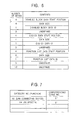
- a boot block format of the memory is shown in Fig. 5.
- page 0 consists of a 388-byte header, a 48-byte system entry, and a 98-byte boot & attribute information.
- Page 1 includes disabled block data.
- Page 2 includes a 256-byte card information structure (CIS) and a 256-byte identity drive information (IDI).
- Page 3 includes a function list information entry in which a list of installed functions is recorded.
- the header on page 0 includes information such as the block ID, a format version, and the number of entries.
- the system entry includes information concerning data from page 1 onward. Specifically, a start position for the disabled block data is provided in the first 4 bytes of the system entry. In the next 4 bytes, the data size of the disabled block data is provided. In the next 1 byte, the ID of the disabled block data is provided. The next 3 bytes are undefined.
- Definitions of the CIS/IDI data are provided in the next 12 bytes of the system entry, as in the information concerning the disabled block data. Specifically, a start position for the CIS/IDI data is provided in the first 4 bytes of the 12 bytes. In the next 4 bytes, the data size of the CIS/IDI data is provided. In the next 1 byte, the ID of the CIS/IDI data is provided. The next 3 bytes are undefined.
- a start position for the function list data is provided in first 4 bytes of the 12 bytes.
- the data size of the function list data is provided in the next 4 bytes.
- the ID of the function list data is provided in the next 1 byte.
- the next 3 bytes are undefined.
- the next 12 bytes are undefined. In this manner, definitions of the function list data are provided in the system entry area.
- function list data shown in Fig. 7 is provided. Specifically, in the function list data, a category number indicating an installed function and a class number corresponding to the category number are provided.
- Fig. 7 shows a case in which the function of the LAN (Ethernet) connecting device and the function of the communication device (Bluetooth) are provided.
- the main unit 100 In order that the main unit 100 obtains the function list data in the electronic device 200, the main unit 100 assumes that the electronic device 200 has a memory function and reads the system entry area. If the reading is performed, it is possible to determine that the electronic device 200 at least has a memory function. In accordance with the definitions provided in the system entry area, the function list data is read. As a result, the function list data in the electronic device 200 can be obtained.
- the main unit 100 writes the category numbers one by one in the write register at the address "06". When the same category number is returned to the read register at the address "06", it is possible to determine that the function is installed in the electronic device 200.
- the main unit 100 can recognize in advance functions installed in the electronic device 200. It is thus possible to prevent unnecessary operations and malfunctions of the main unit 100.
- the main unit 100 checks a recognized function installed in the electronic device 200 with a function thereof and determines that only a matching function is executable. Hence, it is possible to prevent unnecessary operations and malfunctions such as activation of an inexecutable function.
- Recognition of a function installed in the electronic device 200 can be performed by writing, by the main unit 100, the category numbers included in the main unit 100 one by one in the write register at the address "06". Determination is performed whether the same category number is returned to the read register at the address "06". If the determination is affirmative, it is determined that the function is installed in the electronic device 200. Alternatively, before performing necessary functions, recognition of the functions can be respectively performed in a similar manner.
- an electronic device is removably provided with respect to a main unit.
- the electronic device exchanges arbitrary data with the main unit and performs a plurality of functions.
- the electronic device has a register for performing setting when a function is executed. In a predetermined section of the register, a write area, in which the code of a function requested by the main unit is written, and a read area, in which the code of a function selected in the electronic device and the code associated therewith are read, are provided.
Landscapes
- Engineering & Computer Science (AREA)
- Software Systems (AREA)
- Theoretical Computer Science (AREA)
- Physics & Mathematics (AREA)
- General Engineering & Computer Science (AREA)
- General Physics & Mathematics (AREA)
- Storage Device Security (AREA)
- Techniques For Improving Reliability Of Storages (AREA)
- Information Transfer Systems (AREA)
- Facsimiles In General (AREA)
Abstract
Description
Claims (10)
- A control method comprising:a providing step of providing a register which has a predetermined write area and a read area, the register performing setting when a function is executed;a writing step of writing a code of a function requested by a main unit in the write area of the register; anda reading step of reading a code of a function to be executed and a code associated therewith in the read area of the register.
- A control method according to Claim 1, wherein, when the function includes a memory function, a list of the code of the function to be executed and a code associated therewith is provided at a predetermined address in the memory function.
- A control method according to Claim 2, wherein, by gaining access to the predetermined address, the main unit is notified of the function to be executed.
- A control method according to Claim 1, wherein, by writing, by the main unit, a code of an arbitrary function in the write area, and by reading a code of a function selected in the electronic device and a code associated therewith, the main unit is notified of the function to be executed.
- A control method according to Claim 4, wherein the main unit enables the function based on the notification.
- An electronic device, which is removably provided with respect to a main unit, for exchanging data with the main unit and for executing a plurality of functions, comprising:a register for performing setting when the functions are executed,wherein, in a predetermined section of the register, a write area, in which a code of a function requested by the main unit is written, and a read area, in which a code selected in the electronic device and a code associated therewith are read, are provided.
- An electronic device according to Claim 6, wherein, when the functions include a memory function, a list of codes of the functions to be executed and codes associated therewith is provided at a predetermined address in the memory function.
- An electronic device according to Claim 7, wherein, by gaining access to the predetermined address, the main unit is notified of the function to be executed.
- An electronic device according to Claim 6, wherein, by writing, by the main unit, a code of an arbitrary function in the write area, and by reading a code of a function selected in the electronic device and a code associated therewith in the read area, the main unit is notified of the function to be executed.
- An electronic device according to Claim 9, wherein the main unit enables the function based on the notification.
Applications Claiming Priority (4)
| Application Number | Priority Date | Filing Date | Title |
|---|---|---|---|
| JP2000111030 | 2000-04-12 | ||
| JP2000111030 | 2000-04-12 | ||
| JP2001058598A JP5090591B2 (en) | 2000-04-12 | 2001-03-02 | Electronic device control method, electronic device, and function recognition method of electronic device |
| JP2001058598 | 2001-03-02 |
Publications (3)
| Publication Number | Publication Date |
|---|---|
| EP1146421A2 true EP1146421A2 (en) | 2001-10-17 |
| EP1146421A3 EP1146421A3 (en) | 2001-10-24 |
| EP1146421B1 EP1146421B1 (en) | 2007-01-10 |
Family
ID=26589971
Family Applications (1)
| Application Number | Title | Priority Date | Filing Date |
|---|---|---|---|
| EP01303378A Expired - Lifetime EP1146421B1 (en) | 2000-04-12 | 2001-04-11 | Removable electronic device to enhance the functionality of a main processor and control method therefor |
Country Status (9)
| Country | Link |
|---|---|
| US (1) | US7287098B2 (en) |
| EP (1) | EP1146421B1 (en) |
| JP (1) | JP5090591B2 (en) |
| KR (1) | KR100815004B1 (en) |
| CN (1) | CN1178130C (en) |
| DE (1) | DE60125854T2 (en) |
| ES (1) | ES2275627T3 (en) |
| MY (1) | MY126148A (en) |
| TW (1) | TWI224913B (en) |
Families Citing this family (9)
| Publication number | Priority date | Publication date | Assignee | Title |
|---|---|---|---|---|
| JP5244037B2 (en) * | 2008-07-15 | 2013-07-24 | パナソニック株式会社 | Memory device, memory device controller |
| JP5728292B2 (en) * | 2011-02-04 | 2015-06-03 | 株式会社東芝 | Memory device and host system |
| JP5395824B2 (en) | 2011-02-16 | 2014-01-22 | 株式会社東芝 | Memory system |
| JP5832963B2 (en) * | 2012-06-29 | 2015-12-16 | 株式会社東芝 | Memory system |
| JP5779148B2 (en) * | 2012-07-06 | 2015-09-16 | 株式会社東芝 | Memory system |
| JP5814871B2 (en) * | 2012-07-06 | 2015-11-17 | 株式会社東芝 | Memory system |
| JP5779147B2 (en) * | 2012-07-06 | 2015-09-16 | 株式会社東芝 | Memory system |
| JP6017379B2 (en) * | 2013-07-12 | 2016-11-02 | 株式会社東芝 | Memory system and host device |
| CN107247599B (en) * | 2017-06-26 | 2020-08-11 | 北京华睿集成科技有限公司 | Instrument driving module and instrument driving method |
Family Cites Families (20)
| Publication number | Priority date | Publication date | Assignee | Title |
|---|---|---|---|---|
| JP3672576B2 (en) * | 1992-07-01 | 2005-07-20 | 株式会社東芝 | Nonvolatile semiconductor memory device |
| JP3256812B2 (en) * | 1992-08-03 | 2002-02-18 | 株式会社日立製作所 | Communication control device and processor device |
| US5790885A (en) * | 1993-09-10 | 1998-08-04 | Oki Electric Industry Co., Ltd. | Method for controlling IC card reader/writer to transmit same character frame upon receiving echo back character indicating an error exists in received character frame |
| US6698654B1 (en) * | 1995-05-09 | 2004-03-02 | Smartmove (Nz) Ltd. | Method of interfacing with data storage card |
| US6111659A (en) * | 1995-09-26 | 2000-08-29 | Matsushita Electric Industrial Co., Ltd. | Digital copier with image scanner apparatus and offline image data and control data interface |
| DE19536169A1 (en) * | 1995-09-29 | 1997-04-03 | Ibm | Multifunctional chip card |
| JPH09114743A (en) * | 1995-10-16 | 1997-05-02 | Nec Corp | Single chip microcomputer |
| US6901299B1 (en) * | 1996-04-03 | 2005-05-31 | Don Whitehead | Man machine interface for power management control systems |
| US5923884A (en) * | 1996-08-30 | 1999-07-13 | Gemplus S.C.A. | System and method for loading applications onto a smart card |
| JP3164001B2 (en) * | 1996-12-04 | 2001-05-08 | 株式会社村田製作所 | PC card device |
| US5901303A (en) * | 1996-12-27 | 1999-05-04 | Gemplus Card International | Smart cards, systems using smart cards and methods of operating said cards in systems |
| US6164549A (en) * | 1997-05-15 | 2000-12-26 | Mondex International Limited | IC card with shell feature |
| JPH10340575A (en) * | 1997-06-04 | 1998-12-22 | Sony Corp | External storage device and its control device, data transmission / reception device |
| JP3356671B2 (en) * | 1997-12-26 | 2002-12-16 | 日本電気テレコムシステム株式会社 | Function expansion device and method in PC card system |
| JP3829504B2 (en) * | 1998-02-16 | 2006-10-04 | 株式会社デンソー | Information processing device |
| JPH11306129A (en) * | 1998-04-22 | 1999-11-05 | Matsushita Electric Ind Co Ltd | PC card |
| JP2000004389A (en) * | 1998-06-15 | 2000-01-07 | Canon Inc | Imaging device and control method thereof, imaging system, information processing device, adapter |
| GB2343269A (en) * | 1998-10-30 | 2000-05-03 | Ericsson Telefon Ab L M | Processing arrangements |
| JP3621315B2 (en) * | 1999-11-22 | 2005-02-16 | Necエレクトロニクス株式会社 | Microprocessor system |
| US6574677B1 (en) * | 2000-02-23 | 2003-06-03 | Inventec Corporation | Method for using smart card on HPC |
-
2001
- 2001-03-02 JP JP2001058598A patent/JP5090591B2/en not_active Expired - Fee Related
- 2001-04-10 TW TW090108570A patent/TWI224913B/en not_active IP Right Cessation
- 2001-04-10 MY MYPI20011720A patent/MY126148A/en unknown
- 2001-04-11 ES ES01303378T patent/ES2275627T3/en not_active Expired - Lifetime
- 2001-04-11 EP EP01303378A patent/EP1146421B1/en not_active Expired - Lifetime
- 2001-04-11 DE DE60125854T patent/DE60125854T2/en not_active Expired - Lifetime
- 2001-04-11 KR KR1020010019227A patent/KR100815004B1/en not_active Expired - Fee Related
- 2001-04-12 US US09/834,025 patent/US7287098B2/en not_active Expired - Fee Related
- 2001-04-12 CN CNB011166312A patent/CN1178130C/en not_active Expired - Fee Related
Also Published As
| Publication number | Publication date |
|---|---|
| EP1146421B1 (en) | 2007-01-10 |
| DE60125854D1 (en) | 2007-02-22 |
| JP2001356885A (en) | 2001-12-26 |
| CN1317767A (en) | 2001-10-17 |
| US7287098B2 (en) | 2007-10-23 |
| DE60125854T2 (en) | 2007-09-06 |
| EP1146421A3 (en) | 2001-10-24 |
| KR100815004B1 (en) | 2008-03-18 |
| MY126148A (en) | 2006-09-29 |
| JP5090591B2 (en) | 2012-12-05 |
| US20020004864A1 (en) | 2002-01-10 |
| ES2275627T3 (en) | 2007-06-16 |
| TWI224913B (en) | 2004-12-01 |
| KR20010098508A (en) | 2001-11-08 |
| CN1178130C (en) | 2004-12-01 |
Similar Documents
| Publication | Publication Date | Title |
|---|---|---|
| US5687346A (en) | PC card and PC card system with dual port ram and switchable rewritable ROM | |
| US6237091B1 (en) | Method of updating firmware without affecting initialization information | |
| EP0628908A1 (en) | PCMCIA interface using shared memory | |
| JPH06276249A (en) | Transmission control system | |
| EP1146421A2 (en) | Control method and electronic device to enhance the functionality of a main processor | |
| KR20020036717A (en) | Microcomputer and method for controlling the same | |
| KR100538193B1 (en) | Integrated circuit for protocol control | |
| JPH0567028A (en) | Information processing equipment | |
| JPH10198463A (en) | Automatic operating condition setting circuit | |
| JP2002215375A (en) | Image forming apparatus, control method of image forming apparatus, and program for causing computer to execute the method | |
| US5987534A (en) | Radio selective paging receiver provided with an I/O memory card which can be easily upgraded to include new attributes | |
| JPH1145206A (en) | Electronic device, memory activation method, and recording medium recording memory activation program | |
| JP2930259B2 (en) | Portable electronic devices | |
| CN117708004A (en) | Method for reading information of adapter cards with different specifications and substrate management control module | |
| JP4784006B2 (en) | Electronics | |
| EP1158390A1 (en) | Electronic expansion device, unit using the same, and system | |
| JP5030339B2 (en) | Electronics | |
| JP7424536B1 (en) | Electronic information storage medium, IC chip, IC card, communication parameter transmission method, and program | |
| JP4001652B2 (en) | IC card | |
| JPH04205291A (en) | Ic card and information transmitting system | |
| JPH0887896A (en) | Card-shaped circuit block and writing method thereof | |
| JPH0822512A (en) | IC card usage method and IC card | |
| JPH0365368A (en) | Thermal printer | |
| JPS63261599A (en) | Copying system for set value to nonvolatile memory | |
| JPS63196931A (en) | Self-diagnosing system for printer device |
Legal Events
| Date | Code | Title | Description |
|---|---|---|---|
| PUAI | Public reference made under article 153(3) epc to a published international application that has entered the european phase |
Free format text: ORIGINAL CODE: 0009012 |
|
| PUAL | Search report despatched |
Free format text: ORIGINAL CODE: 0009013 |
|
| AK | Designated contracting states |
Kind code of ref document: A2 Designated state(s): DE ES FR GB Kind code of ref document: A2 Designated state(s): AT BE CH CY DE DK ES FI FR GB GR IE IT LI LU MC NL PT SE TR |
|
| AX | Request for extension of the european patent |
Free format text: AL;LT;LV;MK;RO;SI |
|
| AK | Designated contracting states |
Kind code of ref document: A3 Designated state(s): AT BE CH CY DE DK ES FI FR GB GR IE IT LI LU MC NL PT SE TR |
|
| AX | Request for extension of the european patent |
Free format text: AL;LT;LV;MK;RO;SI |
|
| 17P | Request for examination filed |
Effective date: 20020328 |
|
| AKX | Designation fees paid |
Free format text: DE ES FR GB |
|
| GRAP | Despatch of communication of intention to grant a patent |
Free format text: ORIGINAL CODE: EPIDOSNIGR1 |
|
| RTI1 | Title (correction) |
Free format text: REMOVABLE ELECTRONIC DEVICE TO ENHANCE THE FUNCTIONALITY OF A MAIN PROCESSOR AND CONTROL METHOD THEREFOR |
|
| GRAS | Grant fee paid |
Free format text: ORIGINAL CODE: EPIDOSNIGR3 |
|
| GRAA | (expected) grant |
Free format text: ORIGINAL CODE: 0009210 |
|
| AK | Designated contracting states |
Kind code of ref document: B1 Designated state(s): DE ES FR GB |
|
| REG | Reference to a national code |
Ref country code: GB Ref legal event code: FG4D |
|
| REF | Corresponds to: |
Ref document number: 60125854 Country of ref document: DE Date of ref document: 20070222 Kind code of ref document: P |
|
| REG | Reference to a national code |
Ref country code: ES Ref legal event code: FG2A Ref document number: 2275627 Country of ref document: ES Kind code of ref document: T3 |
|
| ET | Fr: translation filed | ||
| PLBE | No opposition filed within time limit |
Free format text: ORIGINAL CODE: 0009261 |
|
| STAA | Information on the status of an ep patent application or granted ep patent |
Free format text: STATUS: NO OPPOSITION FILED WITHIN TIME LIMIT |
|
| 26N | No opposition filed |
Effective date: 20071011 |
|
| REG | Reference to a national code |
Ref country code: GB Ref legal event code: 746 Effective date: 20091130 |
|
| PGFP | Annual fee paid to national office [announced via postgrant information from national office to epo] |
Ref country code: DE Payment date: 20120420 Year of fee payment: 12 |
|
| PGFP | Annual fee paid to national office [announced via postgrant information from national office to epo] |
Ref country code: FR Payment date: 20120507 Year of fee payment: 12 Ref country code: GB Payment date: 20120419 Year of fee payment: 12 |
|
| PGFP | Annual fee paid to national office [announced via postgrant information from national office to epo] |
Ref country code: ES Payment date: 20120424 Year of fee payment: 12 |
|
| GBPC | Gb: european patent ceased through non-payment of renewal fee |
Effective date: 20130411 |
|
| PG25 | Lapsed in a contracting state [announced via postgrant information from national office to epo] |
Ref country code: DE Free format text: LAPSE BECAUSE OF NON-PAYMENT OF DUE FEES Effective date: 20131101 Ref country code: GB Free format text: LAPSE BECAUSE OF NON-PAYMENT OF DUE FEES Effective date: 20130411 |
|
| REG | Reference to a national code |
Ref country code: FR Ref legal event code: ST Effective date: 20131231 |
|
| REG | Reference to a national code |
Ref country code: DE Ref legal event code: R119 Ref document number: 60125854 Country of ref document: DE Effective date: 20131101 |
|
| PG25 | Lapsed in a contracting state [announced via postgrant information from national office to epo] |
Ref country code: FR Free format text: LAPSE BECAUSE OF NON-PAYMENT OF DUE FEES Effective date: 20130430 |
|
| REG | Reference to a national code |
Ref country code: ES Ref legal event code: FD2A Effective date: 20140716 |
|
| PG25 | Lapsed in a contracting state [announced via postgrant information from national office to epo] |
Ref country code: ES Free format text: LAPSE BECAUSE OF NON-PAYMENT OF DUE FEES Effective date: 20130412 |