Technical Field
The present invention relates to a light-emitting device used as a flat
light source and a flat display.
Background Art
Electric field light-emitting devices, which have self-luminous property
and thus high visibility and excellent display capability and enable high
speed response and low-profile, are now attracting the attention as displays
for flat displays and the like.
Among others, an organic EL device, using organic compound as
phosphor, has characteristic features, as compared with inorganic EL device,
that it can be driven at a low voltage, that it can easily produce an enlarged
area, and that it can easily produce a desired luminous color by an
appropriate choice of coloring matter and, accordingly, the organic EL device
is now vigorously developing as a next-generation display.
The EL device using the organic phosphor generates blue luminescence
for example, through the application of a voltage of 30 volts to an
anthracene evaporated film having thickness of 1 m or less (Thin Solid
Films, 94(1982) 171). However, this device fails to produce sufficient
luminance even when a high voltage is applied thereto, so that it is required
to be further improved to have higher luminous efficiency.
In regard to this, Tang et al. teaches that transparent electrodes
(anode), a hole transport layer, an emission region having electron transport
capabilities, cathode using metal of low work function are laminated for
reduction in voltage and improvement in luminous efficiency, to thereby
produce luminance of 1,000 cd/m2 through the application of a voltage of
10V or less (Appl. Phys. Lett. 51 (1987) 913). Used as the phosphor is tris
(8-quinolinolato) aluminum complex (hereinafter it is referred to as "Alq").
The Alq is an excellent luminophor having both high luminous efficiency
and high electron transport capability.
Further, a device having a three-ply structure wherein an emission
region is sandwiched between a hole transport layer and an electron
transport layer and a device that obtains luminescence from coloring matter
(coumarin derivative or fluorescent dye, such as DCM1, used to the Alq)
doped in the emission region is reported (Jpn. J. Appl. Phys., 27 (1988) L269
and J. Appl. Phys., 65(1989) 3610). The report says that it is discovered
that an adequate choice of the coloring matter can allow luminous color to
change and can produce improved luminous efficiency, as compared with the
non-doped one.
In the devices constructed above, all layers are formed by dry process
such as a vacuum evaporation method. On the other hand, the method has
been proposed of producing the device in the so-called wet deposition process
such as a spin coat method and a cast method (Japanese Laid-open
(unexamined) Patent Publications No. Hei 3-790 and No. Hei 3-171590).
In this method, at least one material for forming the hole transport
layer, the electron transport layer and the emission region is dissolved in
appropriate solvent, together with polymer binder. Then, that solution is
applied onto the electrode to form the emission region and, thereafter, a
further electrode is formed on the emission region in the evaporation
method or a like method. Hereinafter, the organic light-emitting device
thus produced is called "polymer dispersed light-emitting device", in
contrast to the conventional laminated light-emitting device.
When comparing with the organic light-emitting device produced by
the dry process, the polymer dispersed light-emitting device has the
following advantages.
The conventional polymer dispersed light-emitting devices comprise
the emission region in which perinone derivative or tris (8-quinolinolato)
aluminum used as the luminous molecules is dispersed in polyvinyl carbazol
or the emission region in which tris (8-quinolinolato) aluminum and
tetraphenyl benzidine used as the luminous molecules are dispersed in
polycarbonate (Japanese Laid-open (unexamined) Patent Publications No.
Hei 3-790, No. Hei 3-171590).
(First problem)
The polymer dispersed light-emitting device has the advantages
mentioned above, while on the other hand, it has the disadvantage that it is
low in luminous efficiency, as compared with the conventional laminated
light-emitting device.
Specifically, in the laminated light-emitting device, holes are injected
from the anode to the hole transport layer, and electrons are injected from
the cathode to the emission region of the electron transport capability or the
electron transport layer. When these holes and electrons are recombined in
the emission region, excitons are formed, and when the excitons are caused
to transition to the ground state, the emission takes place. It is to be noted
that the electron transport and the hole transport are functionally separated
from each other, so that the recombination of the electron and hole takes
place only in the vicinity of an interface between the adjoining layers. This
can produce the efficient production of the excitons and thus improved
luminous efficiency.
Further, through an appropriate choice of the material of the layers
adjoining the respective electrodes to minimize injection barriers between
the anode and the cathode, the injection of the hole and the electron can be
facilitated, and as such can allow the drive at a low voltage.
In contrast to this, the polymer dispersed light-emitting device mainly
comprises a monolayer, so that the recombination of the hole and electron
and the production of the excitons do not take place locally, differently from
the laminated light-emitting device mentioned above. In addition, the
barriers for the hole and the electron to be injected from the electrodes are
high. These facts make it difficult to improve luminous efficiency.
Thus, the emission site is dispersed over the whole emission region, so
that it is hard to balance the injection of the hole and electron and the
transport of the same. As a result of this, the probability of the
recombination reduces, such that sufficient luminous efficiency is not
produced. This indicates that collection of the recombination region of the
hole and electron into a specific region leads up to improvement in luminous
efficiency.
Though the method of laminating the functionally separated layers is
of effective, as mentioned above, in a polymeric system formed by coating,
solvent contained in polymer solution of a second layer to be laminated over
a first deposited layer must be chosen to prevent the first deposited layer
from being dissolved in that solvent.
In addition, as the laminated layers increase in number, the need to
choose the solvent and the need to choose the material soluble in that
selected solvent arise increasingly. This arises the problem that the range
of choice for the material is further narrowed, thus hindering the effectively
improved efficiency.
(Second problem)
Further, the polymer dispersed light-emitting device involves the
problem that when a color panel is produced, it is difficult to do the
patterning (distribution of application of color). When the color panel is
produced in the dry process such as the vacuum evaporation method,
elements of color can be formed in desired positions by an evaporation mask
being set on a substrate. In contrast to this, in the wet deposition such as
the spin coat method or the cast method, since the emission region is formed
over the whole area of the substrate, the above-mentioned patterning cannot
be performed.
In regard to this, the patterning using an ink-jet method has been
proposed (e.g. Japanese Laid-open (unexamined) Patent Publication No. Hei
10-12377). This proposes that material of the emission region including
polymer or the precursor of polymer is discharged from nozzles by the
ink-jet method to form a desired pattern.
However, the patterning using the conventional ink-jet method
involves the problem that polymer solution or equivalent to be coated is high
in viscosity, so that the nozzles of the ink head are easily plugged up and,
accordingly, it is difficult to form a micropattern.
To solve the problems mentioned above, the present invention has been
made. The present invention provides an organic light-emitting device
capable of producing highly improved luminous efficiency and at the same
time facilitating the patterning even in the polymer dispersed organic
light-emitting device and the producing method thereof.
Disclosure of the Invention
In the light of the current situation, a group of inventions have been
made. The object of the invention is to provide a light-emitting device
having high luminous efficiency.
Although the group of inventions is based on the same or similar
conception, since they are realized by way of different embodiments, the
inventive groups are divided into the first inventive group and the second
inventive group on the basis of their respective relevance in the specification.
In the following, the contents will be explained in order for each division
(each inventive group).
(First inventive group)
After having devoted themselves to the studies in order to attain the
object, the inventors of this application have found that in producing a
polymer dispersed light-emitting device, a polymer layer is first formed and
then luminous molecules, or luminous molecules and charge transport are
penetrated in the polymer layer thus formed, thereby producing a highly
improved luminous efficiency and at the same time facilitating the
patterning.
Specifically, a first aspect of the invention is directed to a
light-emitting device having an emission region between an anode and a
cathode, wherein the emission region comprises material contributable to
emission and a medium for containing the material, and wherein the
material contributable to the emission has a substantially successive
distribution of concentration from the anode side of the emission region
toward the cathode side thereof.
A second aspect of the invention is directed to the light-emitting device
as set forth in the first aspect of the invention, wherein the material
contributable to the emission exhibits the distribution of concentration
according to which any one of the anode side of the emission region and the
cathode side thereof is higher in concentration than the other, and the
concentration reduces from the one side toward the other side successively.
With this constitution, in a region where the material contributable to
the emission in the emission region is high in concentration, the hole
injected from the anode into the emission region and the electron injected
from the cathode into the emission region are recombined. Thus, the
recombination region of the hole and the electron is collected, so that the
recombination efficiency of the electron and the hole is increased and thus
the luminous efficiency is improved.
The terminology "material contributable to emission" is intended to
include, for example, material that form organic binder, charge transport
material and dimmer, excimer, or exciplex to obtain emission therefrom, in
addition to the luminous molecules that emit light by the injection of electric
charge as shown in Embodiments as will be mentioned later. It is noted
here that the terminology of the dimmer means material combined with the
organic binder or the charge transport material in the ground state and the
terminology of the excimer and the exciplex means material caused to react
with the organic binder or the charge transport material in the excitation
state caused by the injection of the charge.
A third aspect of the invention is directed to the light emitting device
as set forth in the first aspect of the invention, wherein the emission region
further comprises charge transport material.
The charge transport capabilities in the emission region are further
improved and thus the recombination efficiency of the electron and the hole
is improved.
A fourth aspect of the invention is directed to the light-emitting device
as set forth in the third aspect of the invention, wherein the charge
transport material has a substantially successive distribution of
concentration from the anode side of the emission region toward the cathode
side thereof.
With this constitution, a region large in hole transport capability and a
region large in electron transport capability are formed in the emission
region, as viewed in a direction extending from the anode side to the cathode
side (layer thickness direction), so that the recombination efficiency of the
electron and the hole is improved.
A fifth aspect of the invention is directed to a light-emitting device
having a charge transport region between an anode and a cathode, wherein
the charge transport region comprises charge transport material and a
medium for containing the charge transport material, and wherein the
charge transport material has a substantially successive distribution of
concentration from the cathode side of the charge transport region toward
the anode side thereof.
With this constitution, a region large in hole transport capability and a
region large in electron transport capability are formed in the emission
region, so that the recombination efficiency of the electron and the hole is
improved. In the constitution above, the charge transport region has
luminescent properties and thus doubles as the emission region.
A sixth aspect of the invention is directed to the light-emitting device
as set forth in the first aspect of the invention, wherein the emission region
includes a region where the material contributable to the emission is not
present.
With this constitution, a region different in carrier transport capability
is formed in the emission region, so that the recombination efficiency of the
electron and the hole is further improved and thus the luminance efficiency
is improved.
A seventh aspect of the invention is directed to the light-emitting
device as set forth in the first aspect of the invention, wherein a part of the
emission region that exhibits the maximum concentration of the material
contributable to the emission is away from the anode and the cathode.
The reason that the part of the emission region that exhibits the
maximum concentration of the material contributable to the emission is
away from the both electrodes is that when the material contributable to the
emission is close to the anode or the cathode, there is the possibility that the
material contributable to the emission may be extinguished without
emitting. The part of the emission region that exhibits the maximum
concentration of the material contributable to the emission is preferable at a
substantially immediate position between the anode and the cathode.
An eighth aspect of the invention is directed to the light-emitting
device as set forth in the fifth aspect of the invention, wherein the charge
transport region includes a region where the charge transport material is
not present.
With this constitution, in the boundary between the region where the
charge transport material is present and the region where the charge
transport material is not present a region, the recombination efficiency of
the electron injected from the cathode and the hole injected from the anode
is further improved and thus the luminance efficiency is improved.
A ninth aspect of the invention is directed to the light-emitting device
as set forth in the fifth aspect of the invention, wherein a part of the charge
transport region that exhibits the maximum concentration of the charge
transport material is away from the anode and the cathode.
A tenth aspect of the invention is directed to the lighting device using
the light-emitting device as set forth in the first aspect of the invention.
With this constitution, the lighting device having improved luminance
efficiency can be provided.
An 11th aspect of the invention is directed to a light-emitting device
having an emission region between an anode and a cathode, wherein the
emission region comprises material contributable to emission and a medium
for containing the material, and wherein the material contributable to the
emission has a distribution of concentration that reduces substantially
successively in a direction parallel to a surface of the cathode and a surface
of the anode from a substantially center of the emission region toward a
periphery thereof.
A 12th aspect of the invention is directed to the light-emitting device
as set forth in the 11th aspect of the invention, wherein there are provided a
number of materials contributable to the emissions and are adjacently
arranged in a direction parallel to a surface of the cathode and a surface of
the anode, and wherein the materials contributable to the emissions are
different from each other in luminous color.
With this constitution, since the concentration is low in regions in the
vicinity of the boundaries between the materials contributable to the
emission, the materials contributable to the emission are prevented from
being mixed with each other. Thus, the light-emitting device that provides
excellent full color display capability with little color mixture is produced.
A 13th aspect of the invention is directed to the light-emitting device
as set forth in the 11th aspect of the invention, wherein the emission region
further comprises charge transport material.
A 14th aspect of the invention is directed to the light-emitting device
as set forth in the 13th aspect of the invention, wherein the charge
transport material has a distribution of concentration that reduces in the
direction parallel to the surface of the cathode and the surface of the anode
from the substantially center of the emission region toward the periphery
thereof.
A 15th aspect of the invention is directed to the light-emitting device
as set forth in the 11th aspect of the invention, wherein the material
contributable to the emission has a substantially successive distribution of
concentration from the cathode side of the emission region toward the anode
side thereof.
With this constitution, since the material contributable to the emission
is made to have the distribution of concentration so that the recombination
region of the hole and the electron is collected, the recombination efficiency
of the electron and the hole is improved and thus the luminance efficiency is
improved.
A 16th aspect of the invention is directed to the light-emitting device
as set forth in the 14th aspect of the invention, wherein the charge
transport material has a substantially successive distribution of
concentration from the cathode side of the emission region toward the anode
side thereof.
With this constitution, the recombination efficiency of the electron and
the hole is further improved and thus the luminance efficiency is improved.
A 17th aspect of the invention is directed to the light-emitting device
as set forth in the 11th aspect of the invention, wherein the emission region
includes a region where the material contributable to the emission is not
present.
An 18th aspect of the invention is directed to the light-emitting device
as set forth in the 11th aspect of the invention, wherein the medium for
containing the material contributable to the emission has charge transport
capability.
A 19th aspect of the invention is directed to the light-emitting device
as set forth in the 11th aspect of the invention, wherein the medium for
containing the material contributable to the emission comprises organic
material.
A 20th aspect of the invention is directed to the light-emitting device
as set forth in the 11th aspect of the invention, wherein the medium
comprises polymer.
With this constitution in which the emission region comprises organic
material, or to be more specific, polymer, the organic light-emitting device
having an improved efficiency is produced.
A 21st aspect of the invention is directed to a display using the
light-emitting device as set forth in the 11th aspect of the invention.
With this constitution, the display having an improved luminous
efficiency is provided.
A 22nd aspect of the invention is directed to a producing method of a
light-emitting device having an emission region between an anode and a
cathode, the producing method comprising: a disposing step of disposing a
medium on the anode or the cathode; and a containing step of allowing
material contributable to emission to be contained in the medium to form
the emission region.
Since this method comprises the step of disposing the medium on the
anode or the cathode and the step of allowing material contributable to
emission to be contained in the medium, it can provide an effective method
when it is difficult to dispose the medium previously containing the material
contributable to the emission on the anode or the cathode.
A 23rd aspect of the invention is directed to a producing method of a
light-emitting device having an emission region between an anode and a
cathode, the producing method comprising a disposing step of disposing a
medium containing charge transport material on the anode or the cathode;
and a containing step of allowing material contributable to emission to be
contained in the medium to form the emission region.
This method enables the charge transport material to be contained in
the medium, and as such can produce the light-emitting device that can
inject and transport the charge with efficiency.
A 24th aspect of the invention is directed to a producing method of a
light-emitting device having an emission region between an anode and a
cathode, the producing method comprising a disposing step of disposing a
medium on the anode or the cathode; and a containing step of allowing
material contributable to emission and charge transport material to be
contained in the medium.
A 25th aspect of the invention is directed to a producing method of a
light-emitting device having an emission region between an anode and a
cathode, the producing method comprising a disposing step of disposing a
medium containing charge transport material on the anode or the cathode;
and a containing step of allowing material contributable to emission and
charge transport material to be contained in the medium.
The charge of the charge transport material contained in the medium
in the disposing step and the charge of the charge transport material in the
containing step may be different from or identical to each other.
A 26th aspect of the invention is directed to a producing method of a
light-emitting device having a charge transport region between an anode
and a cathode, the producing method comprising a disposing step of
disposing a medium on the anode or the cathode; and a containing step of
allowing charge transport material to be contained in the medium.
A 27th aspect of the invention is directed to the producing method of a
light-emitting device as set forth in the 23rd aspect of the invention,
wherein in the containing step, the material contributable to the emission is
penetrated into the medium, whereby it is contained in the medium.
A 28th aspect of the invention is directed to the producing method of a
light-emitting device as set forth in the 24th aspect of the invention,
wherein in the containing step, the material contributable to the emission
and the charge transport material are penetrated into the medium, whereby
they are contained in the medium.
This method provides the light-emitting device that enables the
material contributable to the emission, or the material contributable to the
emission and the charge transport material to have a substantially
successive distribution of concentration from the anode side of the charge
transport region toward the cathode side thereof and vice versa.
A 29th aspect of the invention is directed to the producing method of a
light-emitting device as set forth in the 23rd aspect of the invention,
wherein in the containing step, solution obtained by the material
contributable to the emission being dissolved in solvent is brought into
contact with the medium, whereby the material is penetrated into the
medium.
A 30th aspect of the invention is directed to the producing method of a
light-emitting device as set forth in the 24th aspect of the invention,
wherein in the containing step, solution obtained by the material
contributable to the emission and the charge transport material being
dissolved in solvent is brought into contact with the medium, whereby the
materials are penetrated into the medium.
This method also provides the light-emitting device that enables the
material contributable to the emission, or the material contributable to the
emission and the charge transport material to have a substantially
successive distribution of concentration from the anode side of the charge
transport region toward the cathode side thereof and vice versa.
A 31st aspect of the invention is directed to the producing method of a
light-emitting device as set forth in the 27th aspect of the invention,
wherein in the containing step, the material contributable to the emission is
penetrated into the medium in an ink jet method.
The method above allows the material contributable to he emission to
penetrate into the medium in the ink-jet method, so that when polymer high
in viscosity is used as the precursor of the medium, the need of the
application of the polymer solution and the material contributable to the
emission in the ink-jet method can be eliminated. Therefore, the nozzles of
the ink jet are prevented from being plugged and also fine patterns can be
formed with ease.
(Second inventive group)
On the basis of the concept that collection of the luminous molecules,
which were dispersed over the whole organic layer, to a specific region and
enlargement of the surface area of the organic layer lead to improvement in
efficiency of the polymer-based organic light emitting device, the inventors
of this application disperse the luminous molecules on a front surface of the
organic layer or in a region in the vicinity of the front surface of the same
and thereby solve the problems mentioned above.
Specifically, a 32nd aspect of the invention is directed to a
light-emitting device having an emission region between an anode and a
cathode, wherein the emission region comprises material contributable to
emission, and wherein a collecting means for collecting the material
contributable to the emission to a specific region is provided between the
anode and the cathode.
To be more specific, a 33rd aspect of the invention is directed to a
light-emitting device having an emission region between an anode and a
cathode, wherein at least one of an anode side of the emission region and a
cathode side thereof is made porous, and wherein material contributable to
emission is included in a surface of the emission region which is made
porous.
A 34th aspect of the invention is directed to a light-emitting device
having an emission region between an anode and a cathode, wherein at
least one of an anode side of the emission region and a cathode side thereof
is made porous, and wherein material contributable to emission is included
in a region in the vicinity of a surface of the emission region which is made
porous.
With the constitutions above, the material contributable to emission is
collected to a specific region, or specifically, to a surface of the emission
region which is made porous or to a region in the vicinity of the surface
thereof and also the recombination region of the hole and the electron in
which the material contributable to emission is present is enlarged. Thus,
the emission with improved luminance can be produced.
A 35th aspect of the invention is directed to the light-emitting device
as set forth in the 33rd aspect of the invention, wherein charge transport
material is included in a surface of the emission region which is made
porous.
A 36th aspect of the invention is directed to the light-emitting device
as set forth in the 33rd aspect of the invention, wherein a leveled layer
comprising charge transport material is provided on a surface of the
emission region which is made porous.
With this constitution, leakage of current is prevented and also the
injection and transport of the hole or the electron can be performed with
improved efficiency. Further, the leveled layer can permit the joint surface
of the adjacent anode and cathode to be kept smooth
A 37th aspect of the invention is directed to a light-emitting device
having a charge transport region between an anode and a cathode, wherein
at least one of an anode side of the charge transport region and a cathode
side thereof is made porous.
With this constitution, the charge can be injected from the electrodes
(anode and cathode) into the charge transport region with improved
efficiency. In this constitution, the charge transport region is a region
having the luminescent property and thus doubles as the property of the
emission region.
A 38th aspect of the invention is directed to the light-emitting device
as set forth in the 37th aspect of the invention, wherein the charge
transport region is a hole transport region.
A 39th aspect of the invention is directed to the light-emitting device
as set forth in the 37th aspect of the invention, wherein the charge
transport region is an electron transport region.
A 40th aspect of the invention is directed to the light-emitting device
as set forth in the 33rd aspect of the invention, wherein the emission region
comprises an organic matter.
A 41st aspect of the invention is directed to the light-emitting device as
set forth in the 33rd aspect of the invention, wherein the emission region
comprises polymer.
A 42nd aspect of the invention is directed to a light-emitting device
having an emission region between an anode and a cathode, wherein at
least one of an anode side of the emission region and a cathode side thereof
is roughened, and wherein material contributable to emission is included in
a surface of the roughened emission region.
A 43rd aspect of the invention is directed to a light-emitting device
having an emission region between an anode and a cathode, wherein at
least one of an anode side of the emission region and a cathode side thereof
is roughened, and wherein material contributable to emission is included in
a region in the vicinity of a roughened surface of the emission region.
With these constitutions, the surface area of the recombination region
of the hole and the electron where the material contributable to emission is
present is enlarged, thus producing the emission with improved luminance.
A 44th aspect of the invention is directed to the light-emitting device
as set forth in the 42nd aspect of the invention, wherein a leveled layer
comprising charge transport material is provided on a roughened surface of
the emission region.
A 45th aspect of the invention is directed to a light-emitting device
having a charge transport region between an anode and a cathode, wherein
at least one of an anode side of the charge transport region and a cathode
side thereof is roughened.
With this constitution, the charge can be injected from the electrodes
(anode and cathode) into the charge transport region with improved
efficiency. When he emission region is located over the roughened charge
transport region, the contact area of the emission region and the charge
transport region is enhanced, so that the hole can be injected from the anode
into the emission region with improved efficiency.
A 46th aspect of the invention is directed to the light-emitting device
as set forth in the 45th aspect of the invention, wherein the charge
transport region is a hole transport region.
A 47th aspect of the invention is directed to the light-emitting device
as set forth in the 45th aspect of the invention, wherein the charge
transport region is an electron transport region.
A 48th aspect of the invention is directed to the light-emitting device
as set forth in the 42nd aspect of the invention, wherein the emission region
comprises an organic matter.
A 49th aspect of the invention is directed to the light-emitting device
as set forth in the 42nd aspect of the invention, wherein the emission region
comprises polymer.
A 50th aspect of the invention is directed to a display using the
light-emitting device as set forth in the 33rd aspect of the invention.
A 51st aspect of the invention is directed to a lighting device using the
light-emitting device as set forth in the 33rd aspect of the invention.
With the constitutions above, the display and the lighting device
having improved luminous efficiency can be provided.
A 52nd aspect of the invention is directed to a producing method of a
light-emitting device having an emission region between an anode and a
cathode, the producing method comprising a medium disposing step of
disposing a medium on the anode or the cathode; and a porosity producing
step of making at least a part of the medium porous.
A 53rd aspect of the invention is directed to a producing method of a
light-emitting device having an emission region between an anode and a
cathode, the producing method comprising a medium disposing step of
disposing a medium on the anode or the cathode; a porosity producing step
of making at least one of an anode side of the medium and a cathode side
thereof porous; and a disposing step of disposing material contributable to
emission on a porous surface of the medium, so that the emission region is
formed by the medium and the material contributable to the emission.
A 54th aspect of the invention is directed to a producing method of a
light-emitting device having an emission region between an anode and a
cathode, the producing method comprising a medium disposing step of
disposing a medium on the anode or the cathode; a porosity producing step
of making at least one of an anode side of the medium and a cathode side
thereof porous; a containing step of allowing material contributable to
emission to be contained in a region in the vicinity of a porous surface of the
medium, so that the emission region is formed by the medium and the
material contributable to the emission; and a disposing step of disposing
charge transport material on a porous surface of the medium.
With this constitution, the material contributable to the emission is
collected to the porous surface of the emission region or the region in the
vicinity of the porous surface of the same and also the surface area of he
recombination region of the hole and the electron is enlarged, thus providing
the light-emitting device with improved luminance.
A 55th aspect of the invention is directed to the producing method of a
light-emitting device as set forth in the 53rd aspect of the invention, which
comprises a disposing step of disposing charge transport material on a
porous surface of the emission region.
A 56th aspect of the invention is directed to the producing method of a
light-emitting device as set forth in the 53rd aspect of the invention, which
comprises a leveled layer forming step of forming a leveled layer comprising
charge transport material on the emission region.
With the constitutions above in which the leveled layer is formed over
the emission region, the light-emitting device is provided having the
capabilities that leakage of current is prevented and also the injection and
transport of the hole or the electron can be performed with improved
efficiency and further, the leveled layer can permit the joint surface of the
adjacent anode and cathode to be kept smooth.
A 57th aspect of the invention is directed to the producing method of a
light-emitting device as set forth in the 53rd aspect of the invention,
wherein the disposing step is a step of disposing a medium containing
material soluble in a specified solvent, and the porosity producing step is a
step of eluting the material from the solvent to thereby make the medium
porous.
A 58th aspect of the invention is directed to a producing method of a
light-emitting device having an emission region between an anode and a
cathode, the producing method comprising a medium disposing step of
disposing a medium on the anode or the cathode; and a roughening step of
roughening a part of the medium.
A 59th aspect of the invention is directed to a producing method of a
light-emitting device having an emission region between an anode and a
cathode, the producing method comprising a medium disposing step of
disposing a medium on the anode or the cathode; a roughening step of
roughening at least one of an anode side of the medium and a cathode side
thereof; and a disposing step of disposing material contributable to emission
on a roughened surface of the medium, so that the emission region is formed
by the medium and the material contributable to the emission.
A 60th aspect of the invention is directed to a producing method of a
light-emitting device having an emission region between an anode and a
cathode, the producing method comprising a medium disposing step of
disposing a medium on the anode or the cathode; a roughening step of
roughening at least one of an anode side of the medium and a cathode side
thereof; and a containing step of allowing material contributable to emission
to be contained in a region in the vicinity of a roughened surface of the
medium, so that the emission region is formed by the medium and the
material contributable to the emission.
With the constitutions above, the material contributable to the
emission is collected to the roughened surface of the emission region or the
region in the vicinity of the roughened surface of the same and also the
surface area of the recombination region of the hole and the electron where
the material contributable to the emission is present is enlarged, thus
providing the light-emitting device having the capability of producing
improved luminance.
A 61st aspect of the invention is directed to the producing method of a
light-emitting device as set forth in the 59th aspect of the invention, which
comprises a leveled layer forming step of forming a leveled layer comprising
charge transport material on the emission region.
With this constitution, the light-emitting device is provided having the
capabilities that leakage of current is prevented and also the injection and
transport of the hole or the electron can be performed with improved
efficiency and further, the joint surface of the adjacent anode and cathode
can be kept smooth.
A 62nd aspect of the invention is directed to the producing method of a
light-emitting device as set forth in the 59th aspect of the invention,
wherein the roughening step is a step of roughening the emission region by
dry etching.
The dry etching enables the emission region to be roughened with
ease.
Brief Description of the Drawings
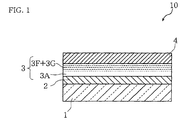
FIG. 1 is a schematic sectional view of an organic light-emitting device
according to an embodiment 1-1 of the present invention;
FIG. 2 shows schematic diagrams illustrating construction of an
organic light-emitting device according to an embodiment 1-2 of the present
invention, FIG. 2(a) is a schematic conceptual diagram of the organic
light-emitting device and FIG. 2(b) is a sectional view taken along the
arrowed line A-A of FIG. 2(a);
FIG. 3 shows schematic sectional views illustrating the producing
method of the organic light-emitting device according to the embodiment 1-2
of the present invention;
FIG. 4 shows schematic sectional views illustrating another example of
the producing method of the organic light-emitting device according to the
embodiment 1-2 of the present invention;
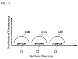
FIG. 5 is a schematic diagram illustrating a distribution of
concentration of an emission region of the organic light-emitting device
according to the embodiment 1-2 of the present invention;
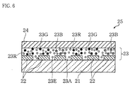
FIG. 6 is a schematic sectional view of an organic light-emitting device
according to an embodiment 1-3 of the present invention;
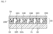
FIG. 7 is a schematic sectional view of an organic light-emitting device
according to an embodiment 1-4 of the present invention;
FIG. 8 is a schematic sectional view of an organic light-emitting device
according to an embodiment 1-5 of the present invention;
FIG. 9 is a schematic sectional view of another example of the organic
light-emitting device according to the embodiment 1-5 of the present
invention;
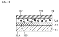
FIG. 10 is a schematic sectional view of yet another example of the
organic light-emitting device according to the embodiment 1-5 of the present
invention;
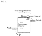
FIG. 11 is an energy level diagram of the organic light-emitting device
according to the embodiment 1-5 of the present invention;
FIG. 12 is an energy level diagram of the organic light-emitting device
according to the embodiment 1-5 of the present invention;
FIG. 13 is an energy level diagram of the organic light-emitting device
according to the embodiment 1-5 of the present invention;
FIG. 14 is an energy level diagram of the organic light-emitting device
according to the embodiment 1-5 of the present invention;
FIG. 15 is a schematic sectional view of an organic light-emitting
device according to an embodiment 2-1 of the present invention;
FIG. 16 shows schematic sectional views illustrating the producing
method of the organic light-emitting device according to the embodiment 2-1
of the present invention;
FIG. 17 is a schematic sectional view showing a variant of the organic
light-emitting device according to the embodiment 2-1 of the present
invention;
FIG. 18 is a schematic sectional view of an organic light-emitting
device according to the embodiment 2-2 of the present invention;
FIG. 19 shows schematic sectional views illustrating the producing
method of the organic light-emitting device according to the embodiment 2-2
of the present invention; and
FIG. 20 is a schematic sectional view showing an organic
light-emitting device according to an embodiment 2-3 of the present
invention.
Best Mode for Carrying out the Invention
(Embodiments of First Inventive Group)
In the following, the first inventive group of the present invention will
be described with reference to the accompanying drawings.
While in the embodiments illustrated below (the same applies to the
second inventive group), description is given on an organic light-emitting
device, the concept of the present invention above is applicable not only to
the organic light-emitting device but also to an inorganic light-emitting
device wherein an emission region is formed, for example, by inorganic
phosphor being dispersed in an organic binder.
[Embodiment 1-1]
FIG. 1 is a schematic sectional view of an organic light-emitting device
according to an embodiment 1-1 of the present invention.
As shown in FIG. 1, an organic light-emitting device 10 comprises an
anode 2 formed on a substrate 1, a cathode 4 arranged in opposition to the
anode 2, and an emission region 3 interposed between the anode 2 and the
cathode 4.
The emission region 3 comprises polymer 3A, luminous molecules 3G
of material contributable to the emission, and charge transport materials 3F.
In FIG. 1, only one kind of luminous molecules is shown.
The luminous molecules 3G and the charge transport materials 3F are
distributed in concentration in a layer thickness direction of the emission
region 3 (from the anode 1 to the cathode 4). Specifically, the concentration
of the luminous molecules 3G and the charge transport materials 3F are
large at a side of the emission region 3 close to the cathode 4 (the upper side
as viewed in the diagram) and are small at a side thereof close to the anode
2 (the lower side as viewed in the diagram). Preferably, the emission
region 3 has a region in the layer thickness direction thereof where neither
the luminous molecules 3G nor the charge transport materials 3F are
provided. In other words, it is preferable that the emission region 3 has, at
the side thereof close to the anode 2, a region where neither the luminous
molecules nor the charge transport material exists but only the polymer 3A
exists.
While it is described that the luminous molecules 3G and the charge
transport materials 3F are distributed in concentration in the layer
thickness direction of the emission region, modification may be made such
that only the luminous molecules 3G are distributed in concentration in the
layer thickness direction of the emission region 3 and the charge transport
materials 3F are uniformly distributed in the layer thickness direction
thereof.
Another modification may also be made of the organic light-emitting
device, such that the emission region 3 comprises only the polymer 3A and
the luminous molecules 3G (not include the charge transport materials 3F)
and the luminous molecules 3G are distributed in concentration in the layer
thickness direction.
An emission mechanism of the organic light-emitting device of the
present invention is as follows. In the organic light-emitting device 10
shown in FIG. 1, when a positive voltage is applied to the anode 2 and a
negative voltage is applied to the cathode 4, the hole is injected into the
emission region 3 from the anode 2 and the electron is injected into the
emission region 3 from the cathode 4. Then, the injected hole flows to the
cathode 4 and the injected electron flows to the anode 2. The hole and the
electron are recombined in the emission region 3, in response to which
fluorescence or phosphorescence is emitted from the luminous molecules 3G
in the emission region 3.
The following points can be cited as major factors for determining
current efficiency of the emission (emission efficiency for the injected
current) include:
Of the factors above, (2) and (3) are practically determined by the
luminous molecules' properties themselves.
On the other hand, the efficiency of recombination of the hole and
electron of (1) is most influenced by the balance between the hole and the
electron. If the hole and the electron are badly balanced, even if they are
injected from the electrode, excess carriers reach the opposite electrode
without being recombined in the emission region, resulting in wasteful
currents that do not contribute to the emission.
If the mobility of the carriers in the emission region is enhanced, then
the hole and the electron flow in a balanced manner and the luminous
efficiency is improved. Specifically, it is preferable that the mobility of the
hole is 1 × 10⁻⁷cm2/V · s or more and the mobility of the electron is 5 ×
10-8cm2/V · s or more.
When viewing from the emission mechanism mentioned above, in the
case where the emission region includes a region of high hole
transportability and a region of high electron transportability with respect
to the layer thickness direction, or specifically, in the case where the hole
transportability is high on the anode side of the emission region and the
electron transportability is high on the cathode side of the same, the hole
and the electron injected from the anode and the cathode respectively are
locally recombined in the vicinity of the interface of the both regions.
Thus, when the luminous molecules 3G and the charge transport
materials 3F are distributed in concentration in the layer thickness
direction, as shown in FIG. 1, or preferably, when the emission region 3
includes a region in which neither the luminous molecules 3G nor the
charge transport materials 3F exists, a region different in carrier
transportability is formed in the emission region 3, so that the
recombination efficiency of the above-noted (1) is further improved and the
emission efficiency is also improved.
[Embodiment 1-2]
FIG. 2 shows schematic diagrams illustrating construction of an
organic light-emitting device according to an embodiment 1-2 of the present
invention. FIG. 2(a) is a schematic conceptual diagram of the organic
light-emitting device and FIG. 2(b) is a sectional view taken along the
arrowed line A-A of FIG. 2(a).
As shown in FIG. 2, an organic light-emitting device 20 is a simple
matrix type one comprising anodes 22 formed on a substrate 21 in a striped
form, an emission region 23 formed on the anodes 22, and cathodes 24
formed on the emission region 23 in a striped form to extend orthogonal to
the anodes 22.
The substrate 21 may be made of any material capable of supporting
the organic light-emitting device 20 of the present invention. A
transparent substrate made of glass or resin film such as polycarbonate,
polymethyl methacrylate, and polyethylene terephthalate, or an opaque
substrate made of silicon can be used as the substrate.
At least either of the anodes 22 and the cathodes 24 must be
transparent or translucent to take out the light generated from the emission
region 23 through the either or both of the electrodes.
While the transparent electrodes made of for example indium tin oxide
(ITO) or tin oxide are often used as the anodes 22 in general, metallic
electrodes made of, for example, Ni, Au, Pt, Pd, may be used. As for the
ITO film, the deposition processes, such as a sputtering, an electron beam
evaporation, an ion plating, is adopted, for the sake of improving the
transparency or reducing the resistivity. The layer thickness is determined
from a required sheet resistance and a required visible light transmittance,
but since the organic light-emitting device is relatively large in drive
current density, the film is often used with the thickness of 1,000 or more,
in order to reduce the sheet resistance.
Laminated electrodes of metal, such as Al, Ag and Au, alloy composed
of metal of low in work function and metal of relatively large in work
function and stable, such as MgAg alloy and AlLi alloy, and alloy composed
of metal of low in work function and metal of high in work function, such as
Li/Al and LiF/Al, can be used as the cathodes 24. These cathodes are
preferably formed in the evaporation or the sputtering.
The anodes 22 and the cathodes 24 are the electrodes extending
orthogonal to each other in the striped form. When a forward voltage is
applied to selected anodes and cathodes, the emission region emits light
with luminance corresponding to the applied voltage at the intersection
points of the both of the electrodes.
While in this embodiment, the substrate 21, the anodes 22, the
emission region 23 and the cathodes 24 are laminated in order from the
bottom, they are not necessarily required to be laminated in this order.
The order of lamination of these, from bottom to top, may be the substrate
21, the cathodes 24, the emission region 23 and the anodes 22.
If only the electrodes on the substrate 21 side or the anodes 22 are
transparent and the cathodes 24 are opaque, then the substrate 21 is
required to be transparent in order to take out the light generated.
Next, description on the emission region 23 will be given. The
emission region 23 comprises polymer 23A, luminous molecules (Red) 23R,
luminous molecules (Green) 23G and luminous molecules (Blue) 23B. The
polymer 23A is seriated in an in-plane direction of the emission region 23,
and a number of luminophors 23R, 23G, 23B are adjacently arranged in the
direction parallel to the cathodes 24 and the anodes 22. The luminophors
23R, 23G, 23B are so distributed in density as to substantially continuously
reduce from around the center of the emission region to the periphery in the
direction parallel to the cathodes 24 and the anodes 22.
Now, description on the producing method of the organic light-emitting
device according to the embodiment 1-2 of the present invention will be
given. FIG. 3 shows schematic sectional views illustrating the producing
method of the organic light-emitting device according to the embodiment 1-2
of the present invention.
While in the embodiment 1-2, the luminous molecules are penetrated
into the polymer, the charge transport material as well as the luminous
molecules may be penetrated into the polymer. Alternatively, the luminous
molecules may be penetrated into the polymer in which the charge transport
material is dispersed.
The method above allows the luminous molecules 23R, 23G and 23B to
penetrate into the polymer in the ink-jet method, so that the need of the
application of the polymer solution of high viscosity in the ink-jet method
can be eliminated. Therefore, the luminous molecules can be applied
without the nozzles of the ink jet being plugged, thus enabling the molecules
to be formed into fine patterns.
Referring now to FIG. 5, description will be given on the configuration
of the emission region of the organic light-emitting device produced in the
producing method mentioned above. FIG. 5 is a schematic diagram
illustrating a distribution of concentration of an emission region of the
organic light-emitting device according to the embodiment 1-2 of the present
invention.
The luminous molecules (Red) 23R, the luminous molecules (Green)
23G and the luminous molecules (Blue) 23B are dispersed over the striped
anodes 22 in the in-plane direction of the emission region 23 (in the
direction parallel to the electrodes), and the distribution of concentration of
each luminous molecule 23R, 23G and 23B becomes the maximum at a
substantially center point over the respective anode 22 and gradually
reduces toward the both ends of the each anode 22, as shown in FIG. 5.
This constitution enables the luminous molecules 23R, 23G, 23B in the
vicinity of their boundaries to be small in concentration. Therefore, the
luminous molecules 23R, 23G, 23B are prevented from being mixed in, thus
providing little color mixture and thus producing an excellent full color
display performance.
Further, the luminous molecules 23R, 23G, 23B are penetrated into
the polymer 23A in the ink-jet method using the ink-jets 27, so that the
concentration of the luminance molecules 23R, 23G, 23B in the emission
region 23 becomes larger on the cathode 24 side than on the anode 22 side.
Consequently, the organic light-emitting device of the embodiment 1-2
can provide increased recombination efficiency of the electron and the hole,
to produce improved luminous efficiency, as is the case with the embodiment
1-1 above.
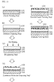
FIG. 4 shows schematic sectional views illustrating another example of
the producing method of the organic light-emitting device according to the
embodiment 1-2 of the present invention.
The procedures shown up to FIG. 4(c) are the same as those of FIG. 3
that the polymer 3A is formed over the substrate 1 on which the anode 2 is
formed.
Then, the luminous molecules 3R, 3G, 3B are penetrated in the
polymer 3A in the following manner.
First, after a mask 8 having opening formed only on the red-color
electrode of the striped anodes 2 of ITO is set on the substrate 1, steaming is
performed by use of solution of red luminous molecules dissolved in the
solvent, as shown in FIG. 4(d), so that the red luminous molecules 3R are
penetrated into the polymer at the desired locations.
Sequentially, the green luminous molecules 3G and the blue luminous
molecules 3B are penetrated in the same manner, as shown in FIG. 4(e),(f).
It is to be noted that any particular limitation is not imposed on the
steaming order of the red, green and blue luminous molecules, and the
luminous molecules may be steamed in any selected order. Preferably, the
luminous molecules are heat-treated after steamed. The heat-treatment
can accelerate the penetration of the luminous molecules 3B-3D into the
polymer 3A. For further acceleration of the penetration of the luminous
molecules into the polymer 3A, it is preferable that the polymer-3A-soluble
liquid is used as the solvent to dissolve the luminous molecules.
Finally, the striped cathodes 4 are formed to extend orthogonal to the
striped anodes 2 in the same manner as in FIG. 3.
While in the embodiment above, the luminous molecules are
penetrated into the polymer, the charge transport material as well as the
luminous molecules may be penetrated into the polymer. Alternatively, the
luminous molecules may be penetrated into the polymer in which the charge
transport material is dispersed.
Also, the method of penetrating the luminous molecules into the
polymer in the printing method can be cited as another example of the
producing method of the organic light-emitting device according to the
present invention.
Specifically, in place of the luminous molecules 3R, 3G, 3B being
penetrated into the polymer 3A in the steaming in FIG. 4(d)-(f), solution of
the luminous molecules is applied to and penetrated into the polymer 3A by
use of an offset printing method or a screen printing method.
In this variant as well, the luminous molecules are preferably
heat-treated after printed, as is the case with the example noted above.
Further, the polymer-3A-soluble liquid is used as the solvent to dissolve the
luminous molecules. Instead of the luminous molecules being penetrated
into the polymer, the charge transport material as well as the luminous
molecules may be penetrated into the polymer. Alternatively, the luminous
molecules may be penetrated into the polymer in which the charge transport
material is dispersed.
[Embodiment 1-3]
FIG. 6 is a schematic sectional view of an organic light-emitting device
according to an embodiment 1-3 of the present invention.
The embodiment 1-3 differs from the embodiment 1-2 in that in
addition to the luminous molecules 23R, 23G, 23B, the charge transport
material 23E are presented in the emission region 23. Here, the polymer
23A and the charge transport material 23E are seriated in the in-plane
direction of the emission region 23. In other words, the charge transport
material 23E is uniformly dispersed in the polymer 23A. The luminous
molecules 23R, 23G, 23B are dispersed over the striped anodes 22,
respectively, as is the case with the embodiment 1-2.
[Embodiment 1-4]
FIG. 7 is a schematic sectional view of an organic light-emitting device
according to an embodiment 1-4 of the present invention.
FIG. 7 differs from FIG. 6 in that the charge transport material 23E
are not seriated in the in-plane direction of the emission region 23, but are
distributed in concentration in the in-plane direction, as is the case with the
luminous molecules 23R, 23G and 23B. Specifically, the charge transport
material 23E are present in large concentration in a region where the
luminous molecules 23R, 23G, 23B are large in concentration.
[Commonalities among Embodiments 1-2 to 1-4]
Polymer having charge transport capabilities (charge transport
polymer) is preferably used as the polymeric material. Among others,
polymer having hole transport capabilities (hole transport polymer) is
preferable. Preferably, the hole transport polymer has the mobility of
carrier of 1 × 10⁻⁷cm2/V • s or more. Particularly preferable is
poly-N-vinylcarbazol.
When the hole transport polymer is used, the electron transport
material is preferably used as the charge transport material. Further, it is
preferable that the electron transport material has the mobility of the
carrier of 5 × 10⁻⁸cm2/V • s or more. Particularly preferable are oxazole
derivative, oxadiazole derivative, triazole derivative, pyrazine derivative,
aldazine derivative, quinolinol complex and derivative thereof. A content of
the electron transport material to the polymer is preferably 30-120 weight%.
With the electron transport material content of less than 30 weight%, the
electron transportability is not sufficient, while on the other hand, with the
electron transport material content of more than 120 weight%, the
dispersibility into the polymer deteriorates.
Fluophor or phosphor that exhibits luminescence in response to the
recombination of the hole and electron may be used as the luminous
molecules. The materials that emit particularly strong fluonescence or
phosphonescence, which may be used, include coloring matters or laser dyes,
such as cyanine dye, merocyanine dye, styrylic dye, anthracene derivative,
porphyrin derivative, phthalocyanine derivative, coumarin, DCM and Nile
red. Preferably used as the luminous molecule is the material having
ionization potential of the luminous molecule smaller than ionization
potential of the hole transport polymer and also electron affinity of the
luminous molecule larger than electron affinity of the electron transport
material.
[Embodiment 1-5]
FIGS. 8-10 are schematic sectional views of the organic light-emitting
device according to an embodiment 1-5 of the present invention. In FIGS.
8-10, 25 designates a hole injection layer, 26 designates an electron injection
layer, 23G designates the luminous molecules, 23H designates hole
transport material, and 23I designates electron transport material.
The hole injection layer 25 is inserted for the purpose of subserving the
injection of the hole from the anode 22 into the emission region 23.
Preferably, the material used for the hole injection layer 25 has the relation
among the ionization potential of the hole injection layer (Ip(h)), the
ionization potential of the polymer (Ip(p)) and the ionization potential of the
anode or the work function (Ip(a)) of the anode being Ip(a)<Ip(h)<Ip(p). It is
particularly preferable that the hole injection layer comprises at least one
material of polyaniline derivative, polythiophene derivative and amorphous
carbon.
The electron injection layer 26 is inserted for the purpose of subserving
the injection of the electron from the cathode 24 into the emission region 23.
Desirably, the material used for the electron injection layer 26 has the
electron affinity or work function smaller than the work function of the
cathode. It is particularly preferable that the electron injection layer
comprises at least one material of dilithium phthalocyanine, disodium
phthalocyanine and organic boron complex compound.
The hole transport material 23H is introduced for the purpose of
subserving the injection of the hole from the anode 22 into the emission
region 23, as is the case with the hole injection layer. However, differently
from the hole injection layer 25, the hole transport material is not inserted
in between the anode 22 and the emission region 23 in the form of a layer,
but is directly dispersed in the emission region.
Preferably; the material used for the hole transport material 23H has
the ionization potential smaller than the ionization potential of the polymer.
A content of the hole transport material to the polymer is preferably 10-120
weight%. With the hole transport material content of less than 10 weight%,
the hole cannot be injected fully, while on the other hand, with the hole
transport material content of more than 120 weight%, the dispersibility into
the polymer deteriorates.
The effects produced by the introduction of the hole injection layer 25,
the electron injection layer 26 and the hole transport material 23H will be
described with reference to the related diagrams. FIGS. 11-14 are energy
level diagrams of the organic light-emitting device according to the present
invention.
FIG. 11 shows an energy level diagram and an operation mechanism of
an organic light-emitting device having the structure of anode/emission
region (hole transport polymer + electron transport material + luminous
molecules (luminescent material))/cathode. FIG. 12 shows an energy level
diagram and an operation mechanism of an organic light-emitting device
having the structure of anode/hole injection layerlemission region (hole
transport polymer + electron transport material + luminous
molecule/cathode. As already noted, when a voltage is applied to the
organic light-emitting device, the hole is injected from the anode into the
emission region and the electron is injected from the cathode into the
emission region. In more detail, as shown in FIG. 11, the both carriers are
injected into the material of smaller injection barrier. In other words, the
hole is injected into the hole transport polymer in the emission region, and
the electron is injected into the electron transport material in the emission
region. It should be noted that the smaller the injection barrier for the
both carriers (hole and electron) become, the more the injection of the
carriers facilitates and the more the driving voltage reduces. This
reduction of the driving voltage can provide improved power efficiency for
emission (emitting efficiency for input power) even when the current
efficiency is identical. For example, when the hole injection layer having
the ionization potential between the anode and the hole transport polymer
is inserted, the hole injection barrier is relaxed, as shown in FIG. 12, and
the driving voltage can also be lowered. Further, when the hole injection
barrier is greater than the electron injection barrier, as shown in FIG. 11,
the hole injection barrier is lowered so that an improved balance between
the injection rate of the hole and the injection rate of the electron is
produced, and as such can allow the current efficiency to be expectably
improved by the aforesaid effects. FIG. 13 shows an energy level diagram
of an organic light-emitting device having the structure of anode/emission
region (hole transport polymer + electron transport material + luminous
molecules)/electron injection layer/cathode. As is the case with the hole
injection barrier, the electron injection barrier can also be lowered by
inserting the electron injection layer smaller in electron affinity than the
cathode, as shown in FIG. 13, thus producing reduction in driving voltage
and improvement in luminous efficiency. FIG. 14 shows an energy level
diagram of an organic light-emitting device having the structure of
anode/emission region (hole transport polymer + hole transport material +
electron transport material + luminous molecules)/cathode. In this case,
since the ionization potential of the hole transport material is smaller than
that of the hole transport polymer, the hole is directly injected into the hole
transport material in the emission region from the anode, as shown in the
diagram, so that the injection barrier is lowered, as compared with the case
of the hole being injected into the hole transport polymer. Hence, as is the
case with the structure of the hole injection layer being inserted, the driving
voltage can be reduced and at the same time the current efficiency can be
expectedly improved.
Of course, the above-noted structures may be combined to provide the
structure wherein both of the hole injection layer and the electron injection
layer are inserted; the structure wherein the emission region comprises the
hole transport polymer + hole transport material + electron transport
material + luminous molecules and further the electron injection layer is
inserted; or the structure wherein the luminous molecules and the charge
transport material are distributed in concentration in the layer thickness
direction of the emission region.
While in the above-mentioned embodiments 1-1 to 1-5, examples of the
simple matrix organic light-emitting device are shown, modification may be
made, such as, for example, forming the light emitting device structured as
mentioned above on the thin film transistor to produce an active matrix
display panel.
Now, experimental examples based on the embodiments mentioned
above will be described in further detail.
(Experimental Example 1)
The organic light-emitting device was produced as mentioned below, in
accordance with the procedures of FIG. 3 illustrated in the aforesaid
Embodiment 1-1.
A glass substrate having thickness of 0.7mm was used as the substrate
1 and ITO was deposited thereon in the form of the anode 2 by the
sputtering method. The ITO was deposited to have thickness of about
1,000 and the sheet resistance was set at about 150Ω/□ . The ITO was
patterned in the striped form having width of 300 µ m by use of photo
lithography.
Then, after the substrate was washed and subjected to oxygen plasma
treatment, poly-N-vinylcarbazol (PVK)(molecular weight of about 28,000)
was deposited thereon as the polymer 3A. The PVK is the hole transport
polymer and the mobility of the carriers is about 2 × 10⁻⁶cm2/V • s. The
deposition was performed in the spin coat method, using the solution in
which 300mg of PVK was dissolved in 30ml of toluene. The spin coat was
performed with spin in a closed state in the conditions of 500rpm/10sec. and
of 1,000rpm/30sec..
Then, the PVK was heat-treated at 110°C for 1 minute by use of a hot
plate. It was about 1,000 in layer thickness.
Then, the luminous molecules were dropped on the ITO electrodes at
desired locations by use of a commercially available ink-jet printer, to form
the emission region. Nile red was used as red luminous molecules (3R),
coumarin 6 was used as green luminous molecules (3G), and coumarin 47
was used as blue luminous molecules (3B). The respective luminous
molecules were discharged from the ink head 7 in the form of solution in
which 1mg of luminous molecules were dissolved 10ml of chloroform.
Every time the luminous molecules were dropped, they were heat-treated at
110°C for 1 minute by use of the hot plate.
Finally, Li/Al laminated electrodes were deposited as the cathodes 4 by
the vacuum evaporation method. The deposition was performed under the
degree of vacuum of about 5×10⁻⁶ Torr. First, Li was allowed to evaporate
by 10 at a rate of about 0.5 /sec. and then Al was allowed to evaporate by
1,500 at a rate of about 30 /sec.. The cathodes was formed into the
striped form orthogonal to the anodes 2 by use of the evaporation mask and
having the width of 300 µ m.
The energy levels of the respective materials are as follows. The
ionization potential of the ITO is 4.9eV, the ionization potential of the PVK
is 5.6eV, the electron affinity is 2.0eV, the ionization potential of Nile red is
5.3eV, the electron affinity is 3.5eV, the ionization potential of coumarin 6 is
5.4eV, the electron affinity is 2.9eV, the ionization potential of coumarin 47
is 5.4eV, and the electron affinity is 2.5eV. The work function of Li is 2.9eV
and the work function of Al is 4.3eV.
When an elemental analysis of the region where the coumarin 6 was
dropped was made with respect to the layer thickness direction, in order to
examine the distribution of concentration of the luminous molecules in the
emission region 3, it was found that the quantity of sulfur contained only in
the coumarin 6 gradually decreased from the cathode side toward the anode
side and there were no coumarin 6 left in the vicinity of the anode.
In the organic light-emitting device thus produced, when a forward
voltage of the order of 10V was applied across the selected striped anode and
cathode, the part (critical area) sandwiched between the both electrodes
emitted light brightly in the respective colors corresponding to the luminous
molecules (Nile red: red, coumarin 6: green, and coumarin 47: blue). Thus,
the simple matrix display capable of emitting light in the desired colors at
desired locations (critical areas) was produced.
The current efficiency of each luminescent color (cd/A), the driving
voltage at a luminance of 100cd/m
2 and the power efficiency (lm/W) at a
luminance of 100cd/m
2 are shown in TABLE 1.
| | Current efficiency (cd/A) | Driving voltage (at 100cd/m2)(V) | Power efficiency (at100cd/m2)(lm/W) |
| | Red | Green | Blue | Red | Green | Blue | Red | Green | Blue |
| Experimental Example 1 | 1.5 | 3.0 | 1.7 | 12.0 | 11.0 | 12.0 | 0.4 | 0.9 | 0.4 |
| Experimental Example 2 | 3.0 | 6.0 | 3.4 | 10.4 | 9.0 | 10.0 | 0.9 | 2.1 | 1.1 |
| Experimental Example 3 | 3.3 | 7.2 | 4.0 | 9.2 | 8.0 | 9.0 | 1.1 | 2.8 | 1.4 |
| Experimental Example 4 | 1.8 | 4.1 | 2.0 | 10.5 | 9.2 | 10.3 | 0.5 | 1.4 | 0.6 |
| Experimental Example 5 | 1.9 | 4.2 | 2.0 | 10.5 | 9.0 | 10.0 | 0.6 | 1.5 | 0.6 |
| Experimental Example 6 | 1.9 | 4.2 | 2.1 | 10.4 | 9.0 | 10.1 | 0.6 | 1.5 | 0.7 |
| Experimental Example 7 | 1.8 | 4.1 | 2.0 | 10.5 | 9.0 | 10.0 | 0.5 | 1.4 | 0.6 |
| Experimental Example 8 | 1.7 | 4.0 | 2.1 | 10.2 | 8.8 | 9.9 | 0.5 | 1.4 | 0.7 |
| Experimental Example 9 | 1.8 | 4.5 | 2.2 | 10.3 | 8.9 | 9.9 | 0.5 | 1.6 | 0.7 |
| Experimental Example 10 | 3.5 | 7.1 | 3.8 | 9.0 | 7.6 | 8.7 | 1.2 | 2.9 | 1.4 |
| Experimental Example 11 | 1.6 | 3.2 | 1.5 | 12.0 | 11.0 | 12.1 | 0.4 | 0.9 | 0.4 |
| Experimental Example 12 | 3.0 | 6.1 | 3.2 | 10.4 | 9.0 | 10.1 | 0.9 | 2.1 | 1.0 |
| Experimental Example 13 | 3.4 | 7.0 | 4.0 | 9.2 | 8.0 | 9.1 | 1.2 | 2.7 | 1.4 |
| Experimental Example 14 | 1.5 | 3.1 | 1.6 | 10.5 | 9.2 | 10.2 | 0.4 | 1.1 | 0.5 |
| Experimental Example 15 | 3.0 | 6.1 | 3.0 | 10.5 | 9.0 | 10.0 | 0.9 | 2.1 | 0.9 |
| Experimental Example 16 | 3.5 | 7.2 | 3.9 | 10.4 | 9.0 | 10.1 | 1.1 | 2.5 | 1.2 |
In Experimental example 1, in place of the PVK being deposited as the
polymer 3A. the PVK in which 2-(4-biphenyl)-5-(4-tert
buthylphenyl)-1,3,4-oxadiazole (PBD) was dispersed. The PBD is the
electron transport material and the mobility of the carriers is about 2×
10-6cm2/V • s. The ionization potential is 6.1eV and the electron affinity is
2.4eV. The deposition was performed in the same conditions as those of the
experimental example 1 by the spin coat method, using the solution in
which 300mg of PVK and 180mg of PBD are dissolved in 30ml of solvent in
which toluene and chloroform were mixed in the proportion 1:1.
The properties of this device are shown in TABLE 1.
(Experimental Example 3)
In Experimental example 1, in place of the luminous molecules being
dropped, the mixed solution of the luminous molecules and the PBD
(electron transport material) was dropped.
Specifically, the solution in which 1mg of Nile red + 100mg of PBD,
1mg of coumarin 6 + 100mg of PBD, and 1mg of coumarin 47 + 100mg of
PBD were respectively dissolved in 30ml of solvent in which toluene and
chloroform were mixed in the proportion 1:1 was dropped on the PVK by the
ink jet method.
The properties of this device are shown in TABLE 1.
(Experimental Example 4)
In Experimental example 1, the hole injection layer was inserted in
between the anode and the emission region.
In short, the device was structured, as shown in FIG. 8. The hole
injection layer was formed by the spin coat method using a commercially
available polythiophene derivative, to have layer thickness of 150 , before
the deposition of the PVK. The ionization potential of the polythiophene
derivative used here is 5.3eV.
The properties of this device are shown in TABLE 1.
(Experimental Example 5)
As a substitution for the polythiophene derivative as the hole injection
layer of the experimental example 4, a commercially available polyaniline
derivative that exhibits equivalent ionization potential to the above-noted
polythiophene derivative was used. The deposition of the polyaniline
derivative was performed in the same manner as in the experimental
example 2, to have layer thickness of 150 .
The properties of this device are shown in TABLE 1.
(Experimental Example 6)
As a substitution for the polythiophene derivative as the hole injection
layer of the experimental example 4, amorphous carbon was used. The
amorphous carbon was formed to have layer thickness of 100 by the
sputtering method. The ionization potential of the amorphous carbon is
5.2eV.
The properties of this device are shown in TABLE 1.
(Experimental Example 7)
In Experimental example 1, the electron injection layer was inserted in
between the emission region and the cathode.
In short, the device was structured, as shown in FIG. 9. Dilithium
phthalocyanine was used and deposited as the electron injection layer by the
vacuum evaporation method after the luminous molecules were dropped
over the PVK. Sequentially, Al was deposited as the cathode. The
electron injection layer and the cathode were formed in the manner that
after dilithium phthalocyanine was deposited 10 at a rate of about 0.3
/sec., Al was deposited 1,500 at a rate of about 30 /sec.. The electron
affinity of dilithium phthalocyanine is 3.0e V.
The properties of this device are shown in TABLE 1.
(Experimental Example 8)
As a substitution for the dilithium phthalocyanine as the electron
injection layer of the experimental example 7, disodium phthalocyanine that
exhibits equivalent electron affinity thereto was used. The deposition of
the disodium phthalocyanine was performed in the same manner as in the
experimental example 7, to have layer thickness of 10 .
The properties of this device are shown in TABLE 1.
(Experimental Example 9)
As a substitution for the dilithium phthalocyanine as the electron
injection layer of the experimental example 7, 4,4,8,8-tetrakis
(1H-pyrazole-1-yl) pyrazabole was used. The deposition of the
4,4,8,8-tetrakis (1H-pyrazole-1-yl) pyrazabole was performed in the same
manner as in the experimental example 7, to have layer thickness of 10 .
The electron affinity of the 4,4,8,8-tetrakis (1H-pyrazole-1-yl) pyrazabole is
2.3eV
The properties of this device are shown in TABLE 1.
(Experimental Example 10)
In the experimental example 3, in place of PVK being deposited as the
polymer 3A, the PVK in which N,N'-diphenyl-N,N'-bis
(3-methylphenyl)-1,1'-biphenyl-4,4'-diamine (TPD) is dispersed as the hole
transport material. In short, the device shown in FIG. 10 was produced.
The ionization potential of TPD is 5.4eV. The deposition was performed in
the same conditions as those of the experimental example 1 by the spin coat
method, using the solution in which 300mg of PVK and 180mg of PBD were
dissolved in 30ml of mixed solvent in which toluene and chloroform were
mixed in the proportion 1:1.
The properties of this device are shown in TABLE 1.
(Experimental Example 11)
In accordance with the procedure of FIG. 4, the organic light-emitting
device was produced. After the procedures until FIG. 4(c) were performed
in the same manner as in the experimental example 1, the luminous
molecules are penetrated into the polymer 3A by steaming, to form the
emission region. The luminous molecules used Nile red, coumarin 6 and
coumarin 47, as is the case with the experimental example 1. The
steaming was performed in the following manner. First, after the mask
having the openings at portions corresponding to the red-color electrodes of
the striped anodes 2 formed of ITO was set on the substrate, the polymer
was subjected to the steam generated by heating the solution in which10mg
of Nile red was dissolved in 10ml of toluene. Further, it was heat-treated
at 110°C for 1 minute by use of a hot plate. Thus, the Nile red was
penetrated into the substrate at the desired positions thereof. Sequentially,
after the mask was shifted in position so that the openings were over the
green-color electrodes, the polymer was subjected to the steam generated by
heating the solution in which 10mg of coumarin 6 was dissolved in 10ml of
toluene and further was heat-treated at 110°C for 1 minute. Sequentially,
after the mask was shifted in position in the same manner, the polymer was
treated by the steaming using the solution in which 10mg of coumarin 47
was dissolved in 10ml of toluene and further was heat-treated at 110°C for 1
minute. Finally, the Li/Al laminated electrodes were deposited as the
cathodes 24 in the vacuum evaporation method in the same manner as in
the experimental example 1.
The properties of this device are shown in TABLE 1.
(Experimental Example 12)
In the experimental example 11, in place of PVK being deposited as the
polymer 3A, the PVK in which 2-(4-biphenyl)-5-(4-tert
buthylphenyl)-1,3,4-oxadiazole (PBD) was dispersed was deposited. The
deposition was performed in the same conditions as those of the
experimental example 1 by the spin coat method, using the solution in
which 300mg of PVK and 180mg of PBD were dissolved in 30ml of mixed
solvent in which toluene and chloroform were mixed in the proportion 1:1.
The properties of this device are shown in TABLE 1.
(Experimental Example 13)
In the experimental example 11, in place of the luminous molecules
being steamed, the mixed solution of the luminous molecules and the PBD
was steamed.
Specifically, the solution in which 1mg of Nile red + 100mg of PBD,
1mg of coumarin 6 + 100mg of PBD, and 1mg of coumarin 47 + 100mg of
PBD were respectively dissolved in 30ml of mixed solvent in which toluene
and chloroform were mixed in the proportion 1:1 was used and steamed on
the PVK.
The properties of this device are shown in TABLE 1.
(Experimental Example 14)
In the experimental example 1, in place of the luminous molecules
being dropped, the luminous molecules were penetrated in the printing
method. After the PVK was deposited on the substrate in the same
procedure as in the experimental example 1, the solution in which 1mg of
Nile red was dissolved in 10mg of toluene was applied to the desired ITO
electrodes in the screen printing method and then was heat-treated at 10°C
for 1 minute by use of the hot plate. Likewise, the solution in which 1mg of
coumarin 6 and coumarin 47 were dissolved in 10ml of toluene was applied
to the desired ITO electrodes in the screen printing method and then was
heat-treated at 110°C for 1 minute by use of the hot plate. Finally, the
Li/Al laminated electrodes were deposited as the cathodes 24 in the vacuum
evaporation method in the same manner as in the experimental example 1.
The properties of this device are shown in TABLE 1.
(Experimental Example 15)
In the experimental example 14, in place of PVK being deposited as
the polymer 3A, the PVK in which 2-(4-biphenyl)-5-(4-tert
buthylphenyl)-1,3,4-oxadiazole (PBD) was dispersed was deposited. The
deposition was performed in the same conditions as those of the
experimental example 1 by the spin coat method, using the solution in
which 300mg of PVK and 180mg of PBD were dissolved in 30ml of mixed
solvent in which toluene and chloroform were mixed in the proportion 1:1.
The properties of this device are shown in TABLE 1.
(Experimental Example 16)
In the experimental example 14, in place of the luminous molecules
being applied in the screen printing method, the mixed solution of the
luminous molecules and the PBD was applied in the screen printing method.
Specifically, the solution in which 1mg of Nile red + 100mg of PBD, 1mg of
coumarin 6 + 100mg of PBD, and lmg of coumarin 47 + 100mg of PBD were
respectively dissolved in 30ml of mixed solvent in which toluene and
chloroform were mixed in the proportion 1:1 was applied onto the PVK in
the screen printing method.
The properties of this device are shown in TABLE 1.
(Embodiments of Second Inventive Group)
The light-emitting device of the second inventive group is
characterized in that it comprises the emission region provided between the
anode and the cathode and comprising material contributable to the
emission and also comprises a collecting means, provided between the anode
and the cathode, for collecting the material contributable to the emission
into a specific region. To be more concrete, the light-emitting device
comprises the emission region provided between the anode and the cathode
and comprising material contributable to the emission; a porous or
roughened region between the anode and the cathode; and material
contributable to the emission which is arranged on as well as in the vicinity
of a front surface of the porous or roughened region.
As mentioned above, the provision of the porous or roughened region
can allow the material contributable to the emission to be collected to a
specific region (on or in the vicinity of the front surface of the porous or
roughened region) and also can enlarge a surface area of the
hole-and-electron recombination region where the material contributable to
the emission is present. This can produce the emission with high
luminance.
The application of the light-emitting device thus constructed to a
display or a lighting device can produce the display or lighting device having
high luminance performance.
In the following, the embodiment 2-1 illustrates the light-emitting
device having the structure in which the emission region is made porous.
The embodiment 2-2 illustrates the structure in which the emission region
is roughened. Further, the embodiment 2-3 illustrates the structure in
which the charge transport region is made porous or is roughened.
[Embodiment 2-1]
FIG. 15 is a schematic sectional view of an organic light-emitting
device according to an embodiment 2-1 of the present invention.
As shown in FIG. 15, an organic light-emitting device 100 comprises
an anode 105 formed on a substrate (not shown), a cathode 101 arranged in
opposition to the anode 105, an emission region 109 arranged between the
anode 105 and the cathode 101, and a leveled layer 102 arranged between
the cathode 101 and the emission region 109.
The emission region 109 comprises an organic layer 104 which is made
porous on the cathode 101 side thereof, and luminance molecules 103
arranged on a front surface of the organic layer 104 thus made porous.
Further, a leveled layer 102 comprising charge transport material is
formed on the front surface of the organic layer 104 and the cathode 101 is
laminated on the leveled layer 102.
This constitution, in which the luminous molecules 103 are collected
on the front surface of the organic layer 104 as was made porous to enlarge
a surface area thereof and also the hole-and-electron recombination region
in which the luminous molecules 103 are present is made porous to enlarge
a surface area thereof, can produce the emission with increased luminance.
In addition, the leveled layer 102 comprising the charge transport material
is provided on the surface of the organic layer 104 as was made porous, thus
producing the results that joint surfaces of adjoining electrodes (cathodes
101) can be kept smooth; that leakage of current can be prevented; and that
the hole or the electron can be injected and transported with efficiency.
Also, the filling of the charge transport material into the porous
organic layer 104 enables the hole or the electron to be injected or
transported with efficiency.
The coloring matters whose quantum efficiency is nearly 1, including
laser dyes such as coumarin 6, DCM and phenoxazone 9, are preferably
used for the luminous molecules 103. In addition to this, fused rings, such
as naphthalene, anthracene, pyrene, and naphthacene, and derivatives
thereof are also preferable. For example, rubrene has quantum efficiency
of nearly 1 and is also an efficient luminous material. In addition, metal
complexes, such as Alq and derivative thereof and beryllium benzoquinoline,
are also preferable.
The charge transport material that is filled in the porous organic layer
104 or forms the leveled layer 102 must transport the charge reverse in
polarity to the charge transported by the porous organic layer 104.
When the porous organic layer 104 is formed as the hole transport
organic layer, the electron transport material is chosen as the charge
transport material. On the other hand, when it is formed as the electron
transport organic layer, the hole transport material is chosen as the charge
transport material.
The electron transport materials that may preferably be used include
low molecular weight material easy to enter the interior of the porous layer.
Metal complex, such as Alq and tris (4-methyl-8-quinolinolato) aluminum,
electron deficient compound, such as 4,4,8,8-tetrakis (1H-pyrazole-1-yl)
pyrazabole, and 3-(2'-benzothiazolyl)-7-diethylaminocoumarin can be cited
as the preferable material. Materials having the hole blocking function,
such as bathocuproine and triazole derivative, are also preferable.
The hole transport materials that may be preferably be used include
derivative having triphenylamine as fundamental skeleton. For example,
tetraphenylbenzidine compound, triphenylamine trimer and benzidine
dimer disclosed by Japanese Laid-open (unexamined) Patent Publication No.
Hei 7-126615, various triphenyldiamine derivatives disclosed by Japanese
Laid-open (unexamined) Patent Publication No. Hei 8-48656, and MTPD
(common name: TPD) disclosed by Japanese Laid-open (unexamined) Patent
Publication No. Hei 7-65958 are preferable.
The hole transport material, when filled in the porous layer, can be
replaced by the electron injection material.
The electron injection materials that may preferably be used include
dilithium phthalocyanine, disodium phthalocyanine, magnesium porphin,
4,4,8,8-tetrakis (1H-pyrazole-1-yl) pyrazabole disclosed by Japanese Patent
Application No. Hei 11-214712. The hole injection material that may
preferably used include copper phthalocyanine,
5,10,15,20-tetraphenyl -21H,23H- porphin copper (In Embodiment 2-2
mentioned later, even when the roughened surface is smoothened to the
order of 10nm, the electron injection material may be replaced by the charge
injection material).
In addition to the low molecular weight material, polymeric material
may be chosen as the material to be filled in the porous layer, but since
there is the possibility that the material could not be fully filled therein by
only the application, some measurement, such as heat-treatment at glass
transition point, should be taken to thoroughly penetrate the material into
the porous layer (In Embodiment 2-2 mentioned later, the polymeric
material may be chosen even for filling the roughened surface).
In consideration of making the organic layer porous, organic polymer is
preferable for the material to form the organic layer 104. Particularly,
when it is made to be porous, the polymer-based organic compound is chosen,
since it is subjected to the wet etching process (In Embodiment 2-2
mentioned later, the organic polymer is preferable even for filling the
roughened surface).
Material for general purpose applications, such as
poly-p-phenylenevinylene (PPV), polyvinyl carbazol (PVK),
polymethylmethacrylate (PMMA), polyfluorene and derivatives thereof can
be used as the organic polymers to form the organic layer. Further, for the
purpose of improving the charge transport capabilities, the electron
transport material and the hole transport material may be mixed. The
material for general purpose applications may be used.
Preferably, the organic layer is formed to have thickness of 10-1,000nm.
Preferably, the thickness of the region to be made porous of the organic layer
falls within about one-third of the whole thickness of the organic layer, or
particularly preferably in the range of 5-50nm. When the organic layer is
reduced in thickness to 10nm or less, short-circuit is caused when a voltage
is applied. On the other hand, when it is increased to 1,000nm or more, the
applied voltage is increased and the luminous efficiency is reduced. Also,
when the region to be made porous is more than one-third of the whole
organic layer or more than 50nm, the organic layer is reduced in density, so
that the charge transport performance is deteriorated and also stiffness and
adhesion of the layer to the substrate is weakened. On the other hand,
when the region to be made porous is less than 5nm, the above-mentioned
effects are not easily produced (In the embodiment 2-2 mentioned later, the
same applies to the region to be roughened). In the applied organic layer, it
is necessary that the uniform layer should be formed by deposition, first,
from the viewpoint of the injection and transport of charge. When viewed
microscopically, the organic polymer layer is rough, but the term of "uniform
layer" used herein means that the layer is uniform when viewed
macroscopically. It is necessary that the roughness of the surface of the
deposited layer should be set within 5nm at least. Making the organic
polymer layer porous and rough means that the roughness of the uniformly
deposited layer is further increased.
Referring now to FIG. 16, the producing method of the organic
light-emitting device will be described. FIG. 16 shows schematic sectional
views illustrating the producing method of the organic light-emitting device
according to the embodiment 2-1 of the present invention.
The proportion of the organic material to be mixed with the organic
polymer is preferable 10-50%. This is because when the proportion of the
organic material is less than 10%, the layer (organic layer) cannot fully be
made porous, while on the other hand, when the proportion of the organic
material is more than 50%, the concentration of the layer is lowered, so that
the charge transport capabilities of the entire layer is deteriorated and the
stiffness and adhesion of the layer to the substrate is weakened. The
proportion of the organic material is further preferably 20-30%.
The organic materials that may be chosen for use include oligomer
produced with low molecular weight for wide selection of the solvent, in
addition to the organic polymer.
The dispersion of the luminous molecules is preferably performed in
the evaporation method. The luminous molecules may be brought into
solution so that they can be steamed. In the method for penetrating the
luminous molecules into the porous organic layer, the luminous molecules
are preferably steamed after dispersed (In the embodiment 2-2 mentioned
later as well, the luminous molecules are preferably steamed after
dispersed).
The organic light-emitting device is enabled to take out the surface
emission by making at least one electrode transparent or translucent.
Usually, the ITO (indium tin oxide) film is often used for the anode serving
as the hole injection electrode. Tin oxide, Ni, Au, Pt and Pd can
additionally be cited as the material therefor. The ITO film is formed by
use of the deposition method, such as sputtering, electron beam evaporation
and ion plating, for the purpose of improving the transparency or reducing
the resistivity.
The film thickness is determined from the required sheet resistance
and visible light transmittance. The organic light-emitting device is
relatively high in driving current density, so that it is often used with
thickness of 100nm or more in order to reduce the sheet resistance.
An alloy comprising a metal of low work function and low electron
injection barrier, such as MgAg alloy or AlLi alloy proposed by Tang et al.,
and a metal of relatively large work function and stable is often used for the
cathode serving as the electron injection electrode. For the purpose of the
metal of low work function being deposited on the organic layer side to
protect the metal of low work function, the metal of large work function may
be laminated thickly. Alternatively, a laminated electrode, such as Li/Al
and LiF/Al, may be used therefor. These cathodes are preferably formed in
the evaporation method or the sputtering method. When the electron
injection material, such as dilithium phthalocyanine, disodium
phthalocyanine, magnesium porphin, 4,4,8,8-tetrakis (1H-pyrazole-1-yl)
pyrazabole, is used for the electrode, the electrode can be formed by only the
metal of large work function and stable. This makes it resistant to reaction
such as oxidizing and thus enables an enhanced life property.
The substrate may be formed of any material that can support the
organic light-emitting device laminating the thin film thereon and is
transparent or translucent to take out the emission generated in the organic
layer. Glass such as Corning 1737 or polyester or other resin film may be
used therefore.
FIG. 17 is a schematic sectional view showing a variant of the organic
light-emitting device according to the embodiment 2-1 of the present
invention.
As shown in FIG. 17, the organic light-emitting device 107 has the
constitution in which the luminous molecules 103 of the material
contributable to the emission are penetrated in the porous organic layer 104
in the vicinity of the front surface. The luminous molecules 103 can be
penetrated in the porous organic layer 104 in the vicinity of the front
surface by steaming.
This constitution enables the luminous molecules 103 to be collected in
the porous organic layer 104 in the vicinity of the front surface thereof and
also enables the surface area in the hole-and-electron recombination region
in which the material contributable to the emission to be enlarged, thus
enabling the emission with high luminance. The luminous molecules may
be disposed on and in the vicinity of the front surface of the organic layer
104.
(Experimental Example 2-1)
Experimental Example 2-1 illustrates an actual example of the organic
light-emitting device of the embodiment 2-1. In the following, the
description thereon will be given.
Polyvinyl carbazol and butyral resin of low degree of polymerization
(available from Sekisui Chemical Co., Ltd., S-LEC B, Part number BL-S)
were dissolved in toluene in the proportion 80:20 by weight, to produce the
solution.
Then, the solution thus produced was deposited on the ITO-deposited
glass substrate in the spin coat method to produce the organic layer having
thickness of 100nm.
The ITO substrate forming thereon the organic layer was dipped in
N,N-dimethylformamide, so that only the butyral resin (S-LEC B) was
dissolved and removed and, thereafter, it was dried at 200°C by heating, to
thereby produce the porous organic layer.
After the substrate was cooled down to room temperature in a vacuum
chamber, the coumarin 6 of laser dyes used as the luminous molecules were
dispersed on it at an evaporation rate of 0.01nm/s for 10 seconds by
resistance heating.
Sequentially, 4,4,8,8-tetrakis (1H-pyrazole-1-yl) pyrazabole used as the
electron injection material was evaporated at the evaporation rate of
0.01nm/s for 1 minute.
Finally, an Al electrode was formed at the evaporation rate of1nm/s to
have layer thickness of about 100nm and thereby the organic light-emitting
device.
When the section of the device was observed by SEM, it was found that
the porous layer having diameter of the order of 3-6nm was formed and the
porous region was filled with the electron injection material. When a direct
current voltage was applied to this device for evaluation purpose, it was
found that the green luminescence of coumarin 6 was obtained and glowed
on stably with current efficiency of 8.0cd/A.
| | Current efficiency (cd/A) |
| Experimental Example 2-1 | 8.0 |
| Experimental Example 2-2 | 8.2 |
| Experimental Example 2-3 | 7.5 |
| Experimental Example 2-4 | 3.2 |
In the organic light-emitting device of the experimental example 2-2,
4,4,8,8-tetrakis (1H-pyrazole-1-yl) pyrazabole was evaporated at the
evaporation rate of 0.1nm/s for 2 minutes to thereby produce a leveled layer,
for the purpose of providing the leveled layer, instead of filling the porous
layer with the electron injection material, in the evaporation of the electron
injection material of the experimental example 2-1.
When the section of the device was observed by SEM, it was found that
the leveled layer was formed on the porous layer having diameter of the
order of 3-6nm. When a direct current voltage was applied to this device
for evaluation purpose, it was found that the green luminescence of
coumarin 6 was obtained and glowed on stably with current efficiency of
8.2cd/A.
(Experimental Example 2-4)
The experimental example 2-4 is for comparison with the experimental
examples 2-1 and 2-2 (the organic layer is not made porous).
Polyvinyl carbazol, 2-(4-biphenyl)-5-(4-t buthylphenyl)-1,3,4
-oxadiazole used as the electron transport material, and coumarin 6 used as
the luminous molecule material were dissolved in a weight ratio of
100:40:0.2 in the mixed solvent with a ratio of toluene to THF of 1:1 to
produce the silution.
Thereafter, the solution was applied to the ITO deposited glass
substrate by use of the spinner, to form the organic layer having thickness of
100nm.
The cathode comprising Li and Al of 1nm used as the electron injection
electrode was formed on that organic layer, to thereby produce the organic
light-emitting device.
When a direct current voltage was applied to this device for evaluation
purpose, it was found that the green luminescence of coumarin 6 was
obtained and the current efficiency was 3.2cd/A, as shown in TABLE 2.
Thus, the organic light-emitting device having the organic layer as was
made porous was dramatically improved in current efficiency, as compared
with the one having the organic layer as was not made porous.
[Embodiment 2-2]
Embodiment 2-2 relates to the organic light-emitting device having the
structure in which the emission region is roughened. FIG. 18 is a
schematic sectional view of an organic light-emitting device according to the
embodiment 2-2 of the present invention
As shown in FIG. 18, an organic light-emitting device 110 comprises
the anode 105, the cathode 101 arranged in opposition to the anode 105, an
emission region 113 arranged between the anode 105 and the cathode 101,
and a leveled layer arranged between the cathode 101 and the emission
region 113.
The emission region 113 comprises an organic layer 120 which is made
porous on the cathode 101 side thereof, and the luminance molecules 103
arranged on the roughened front surface of the organic layer 120.
Further, the leveled layer 102 comprising charge transport material is
formed on the organic layer 120 and the cathode 101 is laminated on the
leveled layer 102.
This constitution, in which the luminous molecules 103 are collected
on the emission region 113 (on the front surface of the organic layer 120)
which is roughened to enlarge its surface area and also the
hole-and-electron recombination region in which the luminous molecules
103 are present is roughened to enlarge its surface area, can produce the
emission with increased luminance. It is to be noted that as is the case
with the embodiment 2-1, the luminous molecules may be penetrated in the
organic layer in the vicinity of the front surface thereof or may alternatively
be arranged on as well as in the vicinity of the front surface of the organic
layer.
Referring now to FIG. 19, the producing method of the organic
light-emitting device will be described. FIG. 19 shows schematic sectional
views illustrating the producing method of the organic light-emitting device
according to the embodiment 2-2 of the present invention.
(Experimental Example 2-3)
Experimental Example 2-3 shows an actual example of the organic
light-emitting device of Embodiment 2-2. Specifically, the solution in which
polyvinyl carbazol was dissolved in toluene was deposited on the
ITO-deposited glass substrate in the spin coat method to produce the
organic layer having thickness of 100nm.
Then, the ITO substrate forming thereon the organic layer was
roughened in the dry etching device of parallel flat-plate type in the
conditions of: an oxygen flow rate of 60sccm; pressure of 40mTorr; and
high-frequency output power of 100W for 1 minute and then was disposed in
the vacuum chamber.
Then, the coumarin 6 of laser dyes used as the luminous molecules
were dispersed on the substrate at an evaporation rate of 0.01nm/s for 10
seconds in the vacuum evaporation method using the resistance heating.
Sequentially, 4,4,8,8-tetrakis (1H-pyrazole-1-yl) pyrazabole used as the
electron injection material was evaporated at the evaporation rate of
0.1nm/s for 2 minutes.
Finally, the Al electrode was formed at the evaporation rate of 1nm/s to
have layer thickness of about 100nm and thereby the organic light-emitting
device.
When the section of the device was observed by SEM, it was found that
the roughened surface of the order of ± 3nm and the leveled layer formed by
the electron injection material were formed in the organic layer. When a
direct current voltage was applied to this device for evaluation purpose, it
was found that the green luminescence of coumarin 6 was obtained and
glowed on stably with current efficiency of 7.5cd/A, as shown in TABLE 2.
Thus, the organic light-emitting device shown in Experimental
example 2-3 was dramatically improved in current efficiency by roughening
the organic layer, as compared with the organic light-emitting device shown
in Experimental example 2-4.
[Embodiment 2-3]
While Embodiments 2-1 and 2-2 relate to the organic light-emitting
devices having the structure in which the emission region is made porous or
roughened to produce improved luminous efficiency, this embodiment 2-3
relates to the organic light-emitting device having the structure in which
the charge transport region is roughened. FIG. 20 is a schematic sectional
view showing an organic light-emitting device according to an embodiment
2-3 of the present invention.
As shown in FIG. 20, an organic light-emitting device 115 comprises
the anode 105, the cathode 101 arranged in opposition to the anode 105, an
emission region 117 arranged between the anode 105 and the cathode 101,
and a charge transport layer 116 arranged between the emission region 117
and the anode 105.
The charge transport layer 116 is roughened at the emission region
117 side by the dry etching. In the structure above, the charge transport
layer 116 is the hole transport layer.
This constitution can provide an enhanced contact area of the emission
region 117 and the charge transport region 116 and an improved injection
efficiency of the holes injected from the anode 105 to the emission region
117.
While in this embodiment, reference is given to the constitution of the
charge transport region being roughened, it is needless to say that the
charge transport region may be made porous to achieve the equivalent effect
to the effect produced by roughening the charge transport region. When
the charge transport layer 116 has luminescent properties, the emission
region 117 is not necessarily needed, but instead at least either of the anode
105 side and the cathode 101 side of the charge transport layer 116 may be
made porous or roughened to produce an improved injection efficiency of the
charge from the electrode, as is the case with the above.
Industrial Applicability
As mentioned above, the constitution of the present invention can
attain the objects of the present invention satisfactorily.
According to the invention of the first inventive group, the luminous
molecules, or the luminous molecules and the charge transport material are
penetrated in the polymer, or the polymer in which the charge transport
material is dispersed, to thereby provide the organic light-emitting device
capable of producing an improved luminous efficiency and at the same time
facilitating the patterning even in the polymer dispersed organic
light-emitting device.
According to the invention of the second inventive group, in the
polymer-based organic light-emitting device, the emission region, which was
commonly diffused over the whole organic layer, is collected to a specific
region and also the hole-and-electron recombination region where the
luminous molecules are present is made porous or roughened to enlarge the
surface area, to thereby produce an improved luminous efficiency.