EP1143772A1 - Large el panel and production method therefor - Google Patents
Large el panel and production method therefor Download PDFInfo
- Publication number
- EP1143772A1 EP1143772A1 EP00961233A EP00961233A EP1143772A1 EP 1143772 A1 EP1143772 A1 EP 1143772A1 EP 00961233 A EP00961233 A EP 00961233A EP 00961233 A EP00961233 A EP 00961233A EP 1143772 A1 EP1143772 A1 EP 1143772A1
- Authority
- EP
- European Patent Office
- Prior art keywords
- display devices
- adjacent
- layer
- circuit section
- display
- Prior art date
- Legal status (The legal status is an assumption and is not a legal conclusion. Google has not performed a legal analysis and makes no representation as to the accuracy of the status listed.)
- Withdrawn
Links
Images




Classifications
-
- H—ELECTRICITY
- H05—ELECTRIC TECHNIQUES NOT OTHERWISE PROVIDED FOR
- H05B—ELECTRIC HEATING; ELECTRIC LIGHT SOURCES NOT OTHERWISE PROVIDED FOR; CIRCUIT ARRANGEMENTS FOR ELECTRIC LIGHT SOURCES, IN GENERAL
- H05B33/00—Electroluminescent light sources
-
- G—PHYSICS
- G09—EDUCATION; CRYPTOGRAPHY; DISPLAY; ADVERTISING; SEALS
- G09F—DISPLAYING; ADVERTISING; SIGNS; LABELS OR NAME-PLATES; SEALS
- G09F9/00—Indicating arrangements for variable information in which the information is built-up on a support by selection or combination of individual elements
- G09F9/30—Indicating arrangements for variable information in which the information is built-up on a support by selection or combination of individual elements in which the desired character or characters are formed by combining individual elements
- G09F9/313—Indicating arrangements for variable information in which the information is built-up on a support by selection or combination of individual elements in which the desired character or characters are formed by combining individual elements being gas discharge devices
-
- H—ELECTRICITY
- H10—SEMICONDUCTOR DEVICES; ELECTRIC SOLID-STATE DEVICES NOT OTHERWISE PROVIDED FOR
- H10K—ORGANIC ELECTRIC SOLID-STATE DEVICES
- H10K59/00—Integrated devices, or assemblies of multiple devices, comprising at least one organic light-emitting element covered by group H10K50/00
- H10K59/10—OLED displays
- H10K59/18—Tiled displays
-
- H—ELECTRICITY
- H10—SEMICONDUCTOR DEVICES; ELECTRIC SOLID-STATE DEVICES NOT OTHERWISE PROVIDED FOR
- H10K—ORGANIC ELECTRIC SOLID-STATE DEVICES
- H10K59/00—Integrated devices, or assemblies of multiple devices, comprising at least one organic light-emitting element covered by group H10K50/00
- H10K59/10—OLED displays
- H10K59/12—Active-matrix OLED [AMOLED] displays
Definitions
- the present invention relates to a large EL panel formed by a plurality of EL display devices such as organic EL panels, which are arranged in a matrix pattern, and also relates to a manufacturing method for the large EL panel.
- Small EL flat panels (EL display devices) driven by polysilicon TFTs are usually laminated on a hard and transparent substrate by an adhesive, etc., in order to maintain the flatness thereof.
- the TFTs control the driving of pixels in the EL display devices individually, so that plane images are displayed.
- the EL display devices as described above are typically two to six inches in diagonal, and provide excellent functions as small image displays.
- a plurality of light sources such as the above-described EL display devices, light bulbs are arranged in a matrix pattern. Each of the light sources functions as a pixel for forming an image.
- the EL display devices having a diagonal size of, for example, several inches should not be a problem.
- liquid crystal display panels have been commonly used as displays for televisions and personal computers.
- a backlight In a liquid crystal display, an additional light source is required as a backlight. Thus, to increase the size of the liquid crystal display, the size of the backlight must also be increased. The present situation, however, is such that when a large (50 to 100 inches in diagonal) and thin display is required, an amount of heat, which increases along with the size of the backlight, will be too large. In addition, the thickness of the display cannot be made thin enough to satisfy the requirement.
- TFT-EL display devices the use of the EL display devices driven by TFTs, which will be referred to as TFT-EL display devices in the following, has been considered.
- the backlights are not required.
- the number of pixels may be increased, and response rate becomes higher, so that high-resolution images may be displayed.
- TFT-EL display devices have not been realized. Accordingly to form a large display panel which is 20 to 100 inches in diagonal, small TFT-EL display devices, which are several inches in diagonal, must be arranged in a matrix pattern.
- a TFT-EL display device is laminated on a flat-type transparent substrate. Accordingly, TFT-EL display devices cannot be arranged in proximity to each other beyond the peripheries of the transparent substrates.
- a TFT array includes not only a pixel section but also a circuit (driver) section for individually controlling the light emission at the pixels.
- the circuit section is disposed at a region outside an image forming area, and prevents the adjacent EL display devices from being arranged in close proximity to each other.
- an object of the present invention is to provide a large EL display panel and a manufacturing method therefor, in which a plurality of EL display devices are arranged in a matrix pattern, and in which a pitch between the pixels in the pixel section of the TFT array is maintained constant.
- the present invention provides a large EL panel comprising a plurality of EL display devices which are arranged in a matrix pattern on a main transparent substrate which is capable of supporting multiple EL display devices, each of the EL display devices including: a base layer over which a luminescent material is applied; an electrode layer which is laminated on one side of the base layer; and a TFT layer including a circuit section in which light emission of the luminescent material is controlled by applying a predetermined voltage between the electrode layer and the TFT layer and a pixel section which is superimposed over the other side of the base layer and which is provided with a plurality of pixels which divide the base layer into sections so that light emission of the luminescent material in each section is individually controlled by generating a potential difference between the electrode layer and the TFT layer at the corresponding section, wherein the circuit section of the TFT layer which is disposed at the region outside a light emitting area is disposed behind the adjacent EL display device so that light emitting areas of the adjacent EL display devices are arranged in proximity to each other
- the present invention also provides a manufacturing method for a large EL panel in which a plurality of EL display panels are used, each of the EL display panels being constructed of the above-described EL display device and a sub transparent substrate for supporting the EL display device, the manufacturing method for the large EL display panel comprising the steps of: removing the EL display devices from the sub transparent substrates; arranging the obtained EL display devices on a main transparent substrate, which is broader than the sub transparent substrate, in a matrix pattern and in a manner such that light emitting areas of the adjacent EL display devices are in proximity to each other; and disposing and fixing the circuit section of the TFT layer, which is disposed at the region outside the light emitting area, behind the adjacent EL display device.
- the EL display devices may be separated from the sub transparent substrates by applying a mechanical or chemical force to adhesive layers which are disposed therebetween, and may be transferred to another substrate.
- Each of the TFT layers has a pixel section and a circuit section.
- the pixel section is superimposed over the light emitting area, so that no problems occur.
- the circuit section is disposed at the periphery, usually at two sides, of the TFT layer, and at the region outside the light emitting area. Accordingly, the circuit section prevents the adjacent EL display devices from being arranged in proximity to each other, so that the ability of the TFTs to display high- resolution images cannot be sufficiently exploited.
- the circuit section is disposed behind the adjacent EL display device, so that a high resolution and large EL display panel may be constructed.
- the manufacturing process of the large EL display panel will be described below.
- the EL display devices are removed from the sub transparent substrates by using the above-described separation and transfer technique.
- the EL display devices are arranged on a main transparent substrate, which is broader than the sub transparent substrate, in a matrix pattern in a manner such that the light emitting areas of the adjacent EL display devices are in proximity to each other.
- the circuit section of the TFT layer which is disposed at the region outside the light emitting area, is disposed and fixed behind the adjacent EL display devices.
- the EL display devices are several inches in diagonal, and the main transparent substrate is 20 to 100 inches in diagonal.
- the predetermined amount of gap between the light emitting areas of the EL display devices is approximately the same as the pitch between pixels provided in the pixel section of the TFT layer.
- the TFT layer is bent at the boundary between the pixel section and the circuit section.
- a step portion for changing the positions of the adjacent EL display devices in the thickness direction may be provided so as to dispose the circuit section behind the adjacent EL display device.
- the adjacent EL display devices may be inverted so as to arrange the base layers of the adjacent EL display devices in the same plane.
- Fig. 1 shows a large EL display panel 10 according to the present embodiment.
- the EL display devices 14A, 14B, 14C, and 14D have the same construction, and are denoted as EL display devices 14 below when they are generically described.
- the EL display devices 14 which are driven by polysilicon TFTs, are divided into a plurality of pixels, and light emission (and gradation) at each pixel is controlled individually.
- the EL display devices 14 are limited in size: a single EL display device is several (2 to 6) inches in diagonal. Thus, to form a display, which is, for example, a dozen inches to a hundred inches in diagonal, a plurality of EL display devices 14 must be arranged in a matrix pattern.
- a display which is approximately 20 inches in diagonal is constructed by the four EL display devices 14. This size is approximately the same as the size 'A3' according to the Japanese Industrial Standard (JIS).
- JIS Japanese Industrial Standard
- Fig. 3 shows a sectional view of one of the EL display devices 14.
- the EL display device 14 incorporated in the present embodiment is prepared as a product, that is, an EL panel 16, in which the EL display device 14 is laminated on a sub transparent substrate 18 via an adhesive layer 20.
- the EL display device 14 is supported by the sub transparent substrate 18 in a manner such that the EL display device 14 is parallel to the sub transparent substrate 18.
- the EL display device 14 is separated from the sub transparent substrate 16 at the adhesive layer 20, as shown in Fig. 4. By using a separation and transfer technique, only the EL display device 14 is removed from the sub transparent substrate 18.
- the EL display device 14 is constructed of a laminate including a plurality of layers.
- the bottom layer of the EL display device 14 is a TFT layer 22 which includes a pixel section 22P and a circuit section 22C.
- the pixel section 22P is divided in a matrix pattern, and is provided with a plurality of pixels. Light emission of a fluorescent material, which will be described below, at each pixel is controlled individually.
- the circuit section 22C includes a driver for controlling the light emission at each pixel, and is disposed along two adjoining sides of the TFT layer 22.
- a base layer 24 on which the fluorescent material is applied is laminated over the pixel section 22P of the TFT layer 22.
- a transparent electrode layer 26 is laminated so as to cover both the base layer 24 and the circuit section 22C.
- the transparent electrode layer 26 also functions as a protection layer.
- the pixels are divided into groups of three, each group providing three colors, RGB, so that color images may be displayed.
- the circuit section 22C of the TFT layer 22 would cause a large gap between the pixels disposed at the peripheries of two adjacent EL display devices 14.
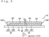
- the TFT layer 22 is bent at the boundary between the circuit section 22C and the pixel section 22P so as to dispose the circuit section 22C behind the adjacent EL display device 14, as shown in Figs. 5 to 7. Accordingly, the pixels at the peripheries of adjacent EL display devices 14 may be arranged in proximity to each other.
- the gap between the pixels at the peripheries of adjacent EL display devices 14 may be reduced to 10 ⁇ m.
- the pitch between the pixels is 50 ⁇ m
- the thickness of the TFT layers is 1 ⁇ m
- the thickness of the EL display devices 14 is 5 ⁇ m.
- a plurality of EL panels 16 is prepared so that a display having a desired diagonal length will be obtained.
- four EL panels 16 are prepared.
- the required EL display device 14 is laminated on the sub transparent substrate 18 by the adhesive layer 20.
- the EL display device 14 is removed from the sub transparent substrate 18 at the adhesive layer 20 by applying the above-described separation and transfer technique.
- the EL display devices 14 obtained from the EL panels 16 are arranged on the main transparent substrate 12 in a matrix pattern (2 x 2).
- the circuit section 22C of the TFT layer 22 would overlap on the adjacent EL display device 14.
- the TFT layer 22 is bent at the boundary between the circuit section 22C and the pixel section 22P so as to dispose the circuit section 22C behind the adjacent EL display device 14.
- the four EL display devices 14 are laminated on the main transparent substrate 12 by the adhesive layer 28 in a similar manner.
- the circuit sections 22C of the TFT layers 22 are disposed behind the adjacent EL display devices 14, so that the gap between the pixels at the peripheries of the adjacent EL display devices 14 may be 10 ⁇ m.
- the four EL display devices 14A, 14B, 14C, and 14D appear to be unified, forming the large EL display panel 10.
- the circuit section 22C of the TFT layer 22 is disposed in a manner such that the TFT layer 22 is not bent at the boundary between the circuit section 22C and the pixel section 22P.
- the main transparent substrate 12 is provided with a step portion 30 formed by the adhesive layer 28 which is used for laminating and fixing the EL display devices 14.
- the step portion 30 is provided so as to change the positions of adjacent EL display devices 14 in the thickness direction.
- the height of the step portion 30 corresponds to the total thickness of the TFT layer 22 and the base layer 24. Accordingly, the circuit section 22C may be disposed behind the adjacent EL display device 14 without bending the TFT layer 22.
- the circuit section 22C of the TFT layer 22 is also disposed in a manner such that the TFT layer 22 is not bent at the boundary between the circuit section 22C and the pixel section 22P.
- the transparent electrode layer (not shown) is laminated on the main transparent substrate 12 as a first layer.
- the base layer 24 is provided as a second layer
- the TFT layer 22 is provided as a third layer. Accordingly, the transparent electrode layer 26, the base layer 24, and the TFT layer 22 are laminated inversely compared to the manner in the first and the second embodiment.
- the thickness of the pixel section 22P of the TFT layer 22 is double compared to that in the adjacent EL display device 14, which is the standard thickness.
- the circuit section 22C is disposed behind the adjacent EL display device 14 without bending the TFT layer 22.
- the process of bending the TFT layer 22 at the boundary between the circuit section 22C and the pixel section 22P is not required.
- the modifications such as changing of the thickness of the layers are required, the TFT layer 22 does not receive any load, so that problems such as contact failures are avoided.
- Fig. 11 shows a first modification in which the four EL display devices 14 are arranged in proximity to each other.
- four similar EL display devices 14 are prepared, and the two EL display devices 14 disposed in the right side and the two EL display devices 14 disposed in left side are arranged inversely to each other. Accordingly, the circuit sections 22C of the TFT layers 22 are prevented from overlapping on the adjacent EL display devices 14.
- Fig. 12 shows a second modification in which the EL display devices 14 disposed at the right side and at the left side have different constructions. More specifically, the circuit sections 22C are disposed at symmetrical regions in the TFT layers 22. According to such a construction, the circuit sections 22C do not overlap on the adjacent EL display devices 14.
- the large EL display panel 10 is constructed of the four EL display devices 14A, 14B, 14C, and 14D in the present embodiment, it is also possible to construct a larger panel.
- Fig. 13 shows an actual manufacturing process of the EL panel 16 which is used for obtaining the large EL display panel 10.
- the EL display devices 14 are formed by the processes shown in Fig. 13, which are described in order from the top.
- the order of the processes is: forming TFTS ⁇ forming an insulating interlayer ⁇ forming contact holes ⁇ forming a transparent electrode layer ⁇ forming banks ⁇ forming a hole transfer layer ⁇ forming an EL layer ⁇ forming an electrode layer.
- the following effects are obtained by the large EL and the manufacturing method therefor according to the present invention. That is, in the case in which a plurality of EL display devices are arranged in a matrix pattern, the pitch between the pixels provided in the pixel section of the TFT array is maintained constant.
Landscapes
- Physics & Mathematics (AREA)
- General Physics & Mathematics (AREA)
- Engineering & Computer Science (AREA)
- Theoretical Computer Science (AREA)
- Electroluminescent Light Sources (AREA)
- Devices For Indicating Variable Information By Combining Individual Elements (AREA)
Abstract
Description
Claims (10)
- A large EL panel comprising a plurality of EL display devices which are arranged in a matrix pattern on a main transparent substrate which is capable of supporting multiple EL display devices, each of said plurality of EL display devices including: a base layer over which a luminescent material is applied; an electrode layer which is laminated on one side of said base layer; and a TFT layer including a circuit section in which light emission of the luminescent material is controlled by applying a predetermined voltage between said electrode layer and said TFT layer and a pixel section which is superimposed over the other side of said base layer and which is provided with a plurality of pixels which divide said base layer into sections so that light emission of the luminescent material in each section is individually controlled by generating a potential difference between said electrode layer and said TFT layer at the corresponding section,
wherein said circuit section of said TFT layer which is disposed at the region outside a light emitting area is disposed behind the adjacent EL display device so that light emitting areas of the adjacent EL display devices are arranged in proximity to each other with a predetermined amount of gap. - A large EL panel according to Claim 1, wherein said plurality of EL display devices are several inches in diagonal, and said main transparent substrate is 20 to 100 inches in diagonal.
- A large EL panel according to one of Claim 1 and Claim 2, wherein said predetermined amount of gap between the light emitting areas of the adjacent EL display devices is approximately the same as a pitch between pixels provided in said pixel section of said TFT layer.
- A large EL panel according to one of Claim 1 to Claim 3, wherein said TFT layer is bent at the boundary between said pixel section and said circuit section so as to dispose said circuit section of said TFT layer behind the adjacent EL display device.
- A large EL panel according to one of Claim 1 to Claim 3, wherein a step portion for changing the positions of the adjacent EL display devices in the thickness direction is provided so as to dispose said circuit section of said TFT layer behind the adjacent EL display device.
- A large EL panel according to Claim 5, wherein the adjacent EL display devices are inverted so as to arrange the base layers of the adjacent EL display devices in the same plane.
- A manufacturing method for a large EL panel in which a plurality of EL display panels are used, each of said plurality of EL display panels being constructed of an EL display device and a sub transparent substrate for supporting said EL display device in parallel, said EL display device including: a base layer over which a luminescent material is applied; an electrode layer which is laminated on one side of said base layer; and a TFT layer including a circuit section in which light emission of the luminescent material is controlled by applying a predetermined voltage between said electrode layer and said TFT layer and a pixel section which is superimposed over the other side of said base layer and which is provided with a plurality of pixels which divide said base layer into sections so that light emission of the luminescent material in each section is individually controlled by generating a potential difference between said electrode layer and said TFT layer at the corresponding section, said manufacturing method for the large EL display panel comprising the steps of: removing said EL display devices from said sub transparent substrates; arranging the obtained EL display devices on a main transparent substrate, which is broader than said sub transparent substrate, in a matrix pattern and in a manner such that light emitting areas of said adjacent EL display devices are in proximity to each other; and disposing and fixing said circuit section of said TFT layer, which is disposed at the region outside the light emitting area, behind the adjacent EL display device.
- A manufacturing method for a large EL panel according to Claim 7, wherein said circuit section of said TFT layer is fixed in a manner such that said TFT layer is bent at the boundary between said circuit section and said pixel section and said circuit section is disposed behind the adjacent EL display device.
- A manufacturing method for a large EL panel according to Claim 7, wherein the thickness of an adhesive layer used for laminating the EL display devices on said main transparent substrate is changed so as to form a step portion which changes the positions of the adjacent EL display devices in the thickness direction, so that said circuit section is disposed behind the adjacent EL display device.
- A manufacturing method for a large EL panel according to Claim 7, wherein said adjacent EL display devices are inverted, and the thickness of said pixel portion of said TFT layer is increased so as to compensate for the displacement between the base layers of the adjacent EL display devices, which is caused as a result of the inversion, so that said circuit section is disposed behind the adjacent EL display device.
Applications Claiming Priority (3)
| Application Number | Priority Date | Filing Date | Title |
|---|---|---|---|
| JP28084399A JP4009923B2 (en) | 1999-09-30 | 1999-09-30 | EL panel |
| JP28084399 | 1999-09-30 | ||
| PCT/JP2000/006622 WO2001024585A1 (en) | 1999-09-30 | 2000-09-26 | Large el panel and production method therefor |
Publications (2)
| Publication Number | Publication Date |
|---|---|
| EP1143772A1 true EP1143772A1 (en) | 2001-10-10 |
| EP1143772A4 EP1143772A4 (en) | 2006-03-29 |
Family
ID=17630766
Family Applications (1)
| Application Number | Title | Priority Date | Filing Date |
|---|---|---|---|
| EP00961233A Withdrawn EP1143772A4 (en) | 1999-09-30 | 2000-09-26 | LARGE EL PANELS AND THEIR PRODUCTION PROCESS |
Country Status (7)
| Country | Link |
|---|---|
| US (2) | US6642542B1 (en) |
| EP (1) | EP1143772A4 (en) |
| JP (1) | JP4009923B2 (en) |
| KR (1) | KR100398542B1 (en) |
| CN (1) | CN100340137C (en) |
| TW (1) | TW474118B (en) |
| WO (1) | WO2001024585A1 (en) |
Cited By (7)
| Publication number | Priority date | Publication date | Assignee | Title |
|---|---|---|---|---|
| WO2006057801A3 (en) * | 2004-11-23 | 2006-11-09 | Eastman Kodak Co | Tiled oled display |
| US7362046B2 (en) | 2001-11-10 | 2008-04-22 | Image Portal Limited | Partial overlapping display tiles of organic light emitting device |
| WO2011031605A1 (en) * | 2009-09-08 | 2011-03-17 | Global Oled Technology Llc | Tiled display with overlapping flexible substrates |
| US8367440B2 (en) | 2001-07-16 | 2013-02-05 | Semiconductor Energy Laboratory Co., Ltd. | Semiconductor device and peeling off method and method of manufacturing semiconductor device |
| US9854629B2 (en) | 2014-08-08 | 2017-12-26 | Semiconductor Energy Laboratory Co., Ltd. | Display device |
| US10776065B2 (en) | 2014-10-08 | 2020-09-15 | Semiconductor Energy Laboratory Co., Ltd. | Display device comprising two display panels |
| US12048230B2 (en) | 2014-02-11 | 2024-07-23 | Semiconductor Energy Laboratory Co., Ltd. | Display device having overlapping display panels |
Families Citing this family (35)
| Publication number | Priority date | Publication date | Assignee | Title |
|---|---|---|---|---|
| JP2002297066A (en) * | 2001-03-30 | 2002-10-09 | Sanyo Electric Co Ltd | Electroluminescence display device and manufacturing method therefor |
| JP4527068B2 (en) * | 2001-07-16 | 2010-08-18 | 株式会社半導体エネルギー研究所 | Peeling method, semiconductor device manufacturing method, and electronic book manufacturing method |
| JP4567282B2 (en) * | 2001-07-16 | 2010-10-20 | 株式会社半導体エネルギー研究所 | Method for manufacturing light emitting device |
| TW558743B (en) | 2001-08-22 | 2003-10-21 | Semiconductor Energy Lab | Peeling method and method of manufacturing semiconductor device |
| GB0127090D0 (en) * | 2001-11-10 | 2002-01-02 | Image Portal Ltd | Display |
| US6953735B2 (en) | 2001-12-28 | 2005-10-11 | Semiconductor Energy Laboratory Co., Ltd. | Method for fabricating a semiconductor device by transferring a layer to a support with curvature |
| JP4606767B2 (en) * | 2004-04-14 | 2011-01-05 | 共同印刷株式会社 | Method for manufacturing element substrate for display device |
| JP4282533B2 (en) * | 2004-04-19 | 2009-06-24 | 株式会社東芝 | Display device |
| US20060044215A1 (en) * | 2004-08-24 | 2006-03-02 | Brody Thomas P | Scalable tiled display assembly for forming a large-area flat-panel display by using modular display tiles |
| JP4496983B2 (en) * | 2005-02-15 | 2010-07-07 | セイコーエプソン株式会社 | Mobile display module |
| US20070001927A1 (en) * | 2005-07-01 | 2007-01-04 | Eastman Kodak Company | Tiled display for electronic signage |
| CN101523469B (en) | 2005-11-14 | 2012-05-30 | 伊里娜·基留谢夫 | Display module and method for manufacturing spliced display |
| US8223087B2 (en) * | 2006-09-25 | 2012-07-17 | Samsung Electronics Co., Ltd. | Multi-display apparatus and method of manufacturing the same |
| US8080926B2 (en) * | 2006-09-25 | 2011-12-20 | Samsung Electronics Co., Ltd. | Multi-display apparatus and method of manufacturing the same |
| KR20080030262A (en) * | 2006-09-29 | 2008-04-04 | 삼성전자주식회사 | Multi display device |
| KR100922069B1 (en) * | 2007-12-06 | 2009-10-16 | 삼성모바일디스플레이주식회사 | Multi vision display |
| JP4421670B2 (en) * | 2009-01-26 | 2010-02-24 | 株式会社東芝 | Display device |
| EP2487671A1 (en) * | 2009-10-08 | 2012-08-15 | Sharp Kabushiki Kaisha | Light emitting panel device wherein a plurality of panels respectively having light emitting sections are connected , and image display device and illuminating device provided with the light emitting panel device |
| JP5254469B2 (en) * | 2009-12-03 | 2013-08-07 | シャープ株式会社 | Image display device, panel and panel manufacturing method |
| KR101298285B1 (en) * | 2009-12-14 | 2013-08-20 | 엘지디스플레이 주식회사 | Outdoor large area display device and manufacturing the same |
| WO2014129519A1 (en) | 2013-02-20 | 2014-08-28 | Semiconductor Energy Laboratory Co., Ltd. | Peeling method, semiconductor device, and peeling apparatus |
| GB2511549B (en) * | 2013-03-07 | 2020-04-22 | Plastic Logic Ltd | Tiled Displays |
| JP2014182306A (en) * | 2013-03-19 | 2014-09-29 | Japan Display Inc | Display device, electronic equipment and method for manufacturing display device |
| WO2015087192A1 (en) | 2013-12-12 | 2015-06-18 | Semiconductor Energy Laboratory Co., Ltd. | Peeling method and peeling apparatus |
| JP2016009112A (en) * | 2014-06-25 | 2016-01-18 | ソニー株式会社 | Display device |
| KR20170093832A (en) * | 2014-11-28 | 2017-08-16 | 가부시키가이샤 한도오따이 에네루기 켄큐쇼 | Image processing device, display system, and electronic device |
| US10606541B2 (en) | 2015-01-22 | 2020-03-31 | Semiconductor Energy Laboratory Co., Ltd. | Display device and electronic device |
| WO2017038495A1 (en) * | 2015-09-02 | 2017-03-09 | コニカミノルタ株式会社 | Illumination device and method for manufacturing illumination device |
| DE112016004055B4 (en) * | 2015-09-08 | 2024-02-08 | Semiconductor Energy Laboratory Co., Ltd. | DISPLAY DEVICES AND ELECTRONIC DEVICE |
| WO2019021147A1 (en) * | 2017-07-27 | 2019-01-31 | 株式会社半導体エネルギー研究所 | Display panel, display device, input/output device, and information processing device |
| TWI781241B (en) | 2017-11-08 | 2022-10-21 | 美商康寧公司 | Apparatus and methods for assembling a display area |
| KR102578423B1 (en) * | 2018-07-03 | 2023-09-13 | 엘지디스플레이 주식회사 | Multi-panel organic light emitting display device |
| US10629566B1 (en) * | 2019-01-28 | 2020-04-21 | GM Global Technology Operations LLC | Seamlessly integrated soft OLEDs |
| JP7638733B2 (en) * | 2021-03-03 | 2025-03-04 | 東京エレクトロン株式会社 | Display method and control device |
| KR102853019B1 (en) * | 2021-11-12 | 2025-09-01 | 엘지디스플레이 주식회사 | Large-area display device and large-area display device driving system |
Family Cites Families (28)
| Publication number | Priority date | Publication date | Assignee | Title |
|---|---|---|---|---|
| US3861783A (en) * | 1973-06-28 | 1975-01-21 | Hughes Aircraft Co | Liquid crystal display featuring self-adjusting mosaic panel |
| JPS56121014A (en) * | 1980-02-28 | 1981-09-22 | Sharp Corp | Liquid-crystal display device |
| DE3305093A1 (en) | 1983-02-14 | 1984-08-16 | Herion-Werke Kg, 7012 Fellbach | Flow-rate valve |
| JPS59147176U (en) * | 1983-03-23 | 1984-10-01 | 日本電気ホームエレクトロニクス株式会社 | EL display device |
| JPH01297864A (en) | 1988-05-26 | 1989-11-30 | Matsushita Electric Ind Co Ltd | Thin film transistor circuit and method of driving same |
| JPH0661023B2 (en) * | 1988-06-28 | 1994-08-10 | スタンレー電気株式会社 | Dot matrix type EL display device |
| US5164853A (en) * | 1989-04-06 | 1992-11-17 | Ricoh Company, Ltd. | Liquid crystal display panel with plural substrates |
| FR2652655A1 (en) * | 1989-10-04 | 1991-04-05 | Commissariat Energie Atomique | LARGE DIMENSIONAL MATRIX DEVICE FOR TAKING OR RETRIEVING IMAGES. |
| US5475514A (en) * | 1990-12-31 | 1995-12-12 | Kopin Corporation | Transferred single crystal arrayed devices including a light shield for projection displays |
| JPH05205875A (en) | 1992-01-28 | 1993-08-13 | Pioneer Electron Corp | Organic electroluminescence display device |
| JP3164179B2 (en) | 1992-08-11 | 2001-05-08 | 旭化成株式会社 | Rare earth bonded magnet |
| FR2701586B1 (en) * | 1993-02-12 | 1995-03-24 | Souriau Diagnostic Electron | Liquid crystal display device comprising an array of image points. |
| JPH07302685A (en) | 1994-05-10 | 1995-11-14 | Nec Kansai Ltd | Method for manufacturing electroluminescent lamp |
| US5550066A (en) * | 1994-12-14 | 1996-08-27 | Eastman Kodak Company | Method of fabricating a TFT-EL pixel |
| US5801797A (en) * | 1996-03-18 | 1998-09-01 | Kabushiki Kaisha Toshiba | Image display apparatus includes an opposite board sandwiched by array boards with end portions of the array boards being offset |
| JP4619462B2 (en) | 1996-08-27 | 2011-01-26 | セイコーエプソン株式会社 | Thin film element transfer method |
| KR100481994B1 (en) * | 1996-08-27 | 2005-12-01 | 세이코 엡슨 가부시키가이샤 | Stripping method, transfer method of thin film device, and thin film device, thin film integrated circuit device and liquid crystal display device manufactured using the same |
| JP4619461B2 (en) | 1996-08-27 | 2011-01-26 | セイコーエプソン株式会社 | Thin film device transfer method and device manufacturing method |
| US5796452A (en) * | 1997-03-21 | 1998-08-18 | International Business Machines Corporation | Simplified wiring escape technique for tiled display |
| JP3566028B2 (en) * | 1997-05-15 | 2004-09-15 | シャープ株式会社 | Liquid crystal display device and method of manufacturing the same |
| JP3483730B2 (en) * | 1997-05-21 | 2004-01-06 | シャープ株式会社 | Liquid crystal display |
| US6078379A (en) * | 1997-06-13 | 2000-06-20 | Sharp Kabushiki Kaisha | Liquid crystal display device provided with seal material and spacer made of resist |
| US5903328A (en) * | 1997-06-16 | 1999-05-11 | Rainbow Displays, Inc. | Tiled flat-panel display with tile edges cut at an angle and tiles vertically shifted |
| JP3494859B2 (en) * | 1997-10-02 | 2004-02-09 | シャープ株式会社 | Liquid crystal panel and manufacturing method thereof |
| JP4547723B2 (en) | 1998-03-09 | 2010-09-22 | セイコーエプソン株式会社 | Manufacturing method of organic EL display device |
| US6246070B1 (en) * | 1998-08-21 | 2001-06-12 | Semiconductor Energy Laboratory Co., Ltd. | Semiconductor device provided with semiconductor circuit made of semiconductor element and method of fabricating the same |
| JP4366743B2 (en) | 1998-09-11 | 2009-11-18 | ソニー株式会社 | Flat panel display |
| WO2014168171A1 (en) * | 2013-04-11 | 2014-10-16 | 富士電機株式会社 | Semiconductor device and semiconductor device manufacturing method |
-
1999
- 1999-09-30 JP JP28084399A patent/JP4009923B2/en not_active Expired - Fee Related
-
2000
- 2000-09-26 EP EP00961233A patent/EP1143772A4/en not_active Withdrawn
- 2000-09-26 US US09/856,852 patent/US6642542B1/en not_active Expired - Lifetime
- 2000-09-26 CN CNB008032645A patent/CN100340137C/en not_active Expired - Fee Related
- 2000-09-26 WO PCT/JP2000/006622 patent/WO2001024585A1/en not_active Ceased
- 2000-09-26 KR KR10-2001-7006736A patent/KR100398542B1/en not_active Expired - Fee Related
- 2000-09-27 TW TW089119913A patent/TW474118B/en not_active IP Right Cessation
-
2003
- 2003-07-14 US US10/617,746 patent/US6967114B2/en not_active Expired - Fee Related
Cited By (11)
| Publication number | Priority date | Publication date | Assignee | Title |
|---|---|---|---|---|
| US8367440B2 (en) | 2001-07-16 | 2013-02-05 | Semiconductor Energy Laboratory Co., Ltd. | Semiconductor device and peeling off method and method of manufacturing semiconductor device |
| US8415208B2 (en) | 2001-07-16 | 2013-04-09 | Semiconductor Energy Laboratory Co., Ltd. | Semiconductor device and peeling off method and method of manufacturing semiconductor device |
| US9608004B2 (en) | 2001-07-16 | 2017-03-28 | Semiconductor Energy Laboratory Co., Ltd. | Semiconductor device and peeling off method and method of manufacturing semiconductor device |
| US10586816B2 (en) | 2001-07-16 | 2020-03-10 | Semiconductor Energy Laboratory Co., Ltd. | Semiconductor device and peeling off method and method of manufacturing semiconductor device |
| US7362046B2 (en) | 2001-11-10 | 2008-04-22 | Image Portal Limited | Partial overlapping display tiles of organic light emitting device |
| WO2006057801A3 (en) * | 2004-11-23 | 2006-11-09 | Eastman Kodak Co | Tiled oled display |
| WO2011031605A1 (en) * | 2009-09-08 | 2011-03-17 | Global Oled Technology Llc | Tiled display with overlapping flexible substrates |
| US8305294B2 (en) | 2009-09-08 | 2012-11-06 | Global Oled Technology Llc | Tiled display with overlapping flexible substrates |
| US12048230B2 (en) | 2014-02-11 | 2024-07-23 | Semiconductor Energy Laboratory Co., Ltd. | Display device having overlapping display panels |
| US9854629B2 (en) | 2014-08-08 | 2017-12-26 | Semiconductor Energy Laboratory Co., Ltd. | Display device |
| US10776065B2 (en) | 2014-10-08 | 2020-09-15 | Semiconductor Energy Laboratory Co., Ltd. | Display device comprising two display panels |
Also Published As
| Publication number | Publication date |
|---|---|
| EP1143772A4 (en) | 2006-03-29 |
| KR20010080628A (en) | 2001-08-22 |
| WO2001024585A1 (en) | 2001-04-05 |
| JP4009923B2 (en) | 2007-11-21 |
| CN100340137C (en) | 2007-09-26 |
| JP2001100662A (en) | 2001-04-13 |
| US20040014252A1 (en) | 2004-01-22 |
| TW474118B (en) | 2002-01-21 |
| KR100398542B1 (en) | 2003-09-19 |
| CN1339240A (en) | 2002-03-06 |
| US6967114B2 (en) | 2005-11-22 |
| US6642542B1 (en) | 2003-11-04 |
Similar Documents
| Publication | Publication Date | Title |
|---|---|---|
| US6642542B1 (en) | Large EL panel and manufacturing method therefor | |
| US10727439B2 (en) | Display panel for maintaining parallel substrates with constant space and display device including the same | |
| JP5153825B2 (en) | Organic light emitting display device and method for manufacturing the same | |
| CN102484123B (en) | Tile display with overlapping flexible substrates | |
| US7068265B2 (en) | Scan structure in display device, method for driving the display device, and method for manufacturing the same | |
| JP2001100662A5 (en) | ||
| KR101691738B1 (en) | Display device | |
| US7714507B2 (en) | Organic electroluminescence display device having red, green, blue and white pixels | |
| US7362046B2 (en) | Partial overlapping display tiles of organic light emitting device | |
| KR101887533B1 (en) | Organic Light Emitting Diode Display Device | |
| CN114300505A (en) | Light-emitting module and display device | |
| US20250169310A1 (en) | Array substrate and display apparatus | |
| US20050231447A1 (en) | Pixel arrangement in a display system | |
| EP1567910A2 (en) | Display panel and large display using such display panel | |
| JP2016206543A (en) | Multi-split driving display and display device | |
| JP2014106297A (en) | Display panel and display device using the same | |
| TWI326379B (en) | A double-sided liquid crystal display | |
| CN117596974A (en) | Display panels and display devices | |
| KR102761311B1 (en) | Organic Light Emitting Display Device for Top and Bottom Emission | |
| KR20010093018A (en) | Wide Electro- luminescence Display Apparatus using Tiling Technique | |
| CN116193921B (en) | Pixel arrangement structure, metal mask plate, display panel and display device | |
| JP7546474B2 (en) | Multi-Display | |
| KR100747236B1 (en) | Organic electroluminescent display and manufacturing method | |
| JP2005331569A (en) | Display device and electronic device | |
| KR20070003082A (en) | Display device |
Legal Events
| Date | Code | Title | Description |
|---|---|---|---|
| PUAI | Public reference made under article 153(3) epc to a published international application that has entered the european phase |
Free format text: ORIGINAL CODE: 0009012 |
|
| AK | Designated contracting states |
Kind code of ref document: A1 Designated state(s): AT BE CH CY DE DK ES FI FR GB GR IE IT LI LU MC NL PT SE |
|
| 17P | Request for examination filed |
Effective date: 20010829 |
|
| RBV | Designated contracting states (corrected) |
Designated state(s): DE FR GB NL |
|
| A4 | Supplementary search report drawn up and despatched |
Effective date: 20060215 |
|
| RIC1 | Information provided on ipc code assigned before grant |
Ipc: G09F 9/40 20060101ALI20010410BHEP Ipc: H05B 33/14 20060101ALI20010410BHEP Ipc: H01L 27/00 20060101AFI20060209BHEP Ipc: H05B 33/10 20060101ALI20010410BHEP Ipc: G09F 9/30 20060101ALI20010410BHEP |
|
| 17Q | First examination report despatched |
Effective date: 20060529 |
|
| GRAP | Despatch of communication of intention to grant a patent |
Free format text: ORIGINAL CODE: EPIDOSNIGR1 |
|
| RIC1 | Information provided on ipc code assigned before grant |
Ipc: G09F 9/30 20060101ALI20090303BHEP Ipc: H01L 27/32 20060101AFI20090303BHEP Ipc: H05B 33/10 20060101ALI20090303BHEP Ipc: H05B 33/14 20060101ALI20090303BHEP Ipc: G09F 9/40 20060101ALI20090303BHEP |
|
| STAA | Information on the status of an ep patent application or granted ep patent |
Free format text: STATUS: THE APPLICATION HAS BEEN WITHDRAWN |
|
| 18W | Application withdrawn |
Effective date: 20090608 |