EP1143505A2 - Planar isolation technique for integrated circuits - Google Patents
Planar isolation technique for integrated circuits Download PDFInfo
- Publication number
- EP1143505A2 EP1143505A2 EP01202722A EP01202722A EP1143505A2 EP 1143505 A2 EP1143505 A2 EP 1143505A2 EP 01202722 A EP01202722 A EP 01202722A EP 01202722 A EP01202722 A EP 01202722A EP 1143505 A2 EP1143505 A2 EP 1143505A2
- Authority
- EP
- European Patent Office
- Prior art keywords
- region
- oxide
- silicon
- trench
- field oxide
- Prior art date
- Legal status (The legal status is an assumption and is not a legal conclusion. Google has not performed a legal analysis and makes no representation as to the accuracy of the status listed.)
- Granted
Links
- 238000000034 method Methods 0.000 title description 23
- 238000002955 isolation Methods 0.000 title description 3
- XUIMIQQOPSSXEZ-UHFFFAOYSA-N Silicon Chemical compound [Si] XUIMIQQOPSSXEZ-UHFFFAOYSA-N 0.000 claims abstract description 22
- 229910052710 silicon Inorganic materials 0.000 claims abstract description 22
- 239000010703 silicon Substances 0.000 claims abstract description 22
- 239000003989 dielectric material Substances 0.000 claims description 12
- VYPSYNLAJGMNEJ-UHFFFAOYSA-N Silicium dioxide Chemical compound O=[Si]=O VYPSYNLAJGMNEJ-UHFFFAOYSA-N 0.000 claims description 11
- 239000000758 substrate Substances 0.000 claims description 9
- 239000002019 doping agent Substances 0.000 claims description 8
- 230000005684 electric field Effects 0.000 claims description 4
- 230000005669 field effect Effects 0.000 claims description 3
- 230000003993 interaction Effects 0.000 claims description 2
- 229910052814 silicon oxide Inorganic materials 0.000 claims 1
- 238000013461 design Methods 0.000 abstract description 5
- 230000003071 parasitic effect Effects 0.000 abstract description 3
- 229910021420 polycrystalline silicon Inorganic materials 0.000 description 23
- 229920005591 polysilicon Polymers 0.000 description 23
- 238000005530 etching Methods 0.000 description 17
- 239000000463 material Substances 0.000 description 9
- 239000004020 conductor Substances 0.000 description 8
- 230000003647 oxidation Effects 0.000 description 7
- 238000007254 oxidation reaction Methods 0.000 description 7
- 238000005516 engineering process Methods 0.000 description 6
- 238000004519 manufacturing process Methods 0.000 description 6
- 150000004767 nitrides Chemical class 0.000 description 6
- 210000002381 plasma Anatomy 0.000 description 6
- 230000008569 process Effects 0.000 description 6
- 229910052581 Si3N4 Inorganic materials 0.000 description 5
- 238000000151 deposition Methods 0.000 description 5
- 229920002120 photoresistant polymer Polymers 0.000 description 5
- 235000012239 silicon dioxide Nutrition 0.000 description 5
- 239000000377 silicon dioxide Substances 0.000 description 5
- HQVNEWCFYHHQES-UHFFFAOYSA-N silicon nitride Chemical compound N12[Si]34N5[Si]62N3[Si]51N64 HQVNEWCFYHHQES-UHFFFAOYSA-N 0.000 description 5
- QVGXLLKOCUKJST-UHFFFAOYSA-N atomic oxygen Chemical compound [O] QVGXLLKOCUKJST-UHFFFAOYSA-N 0.000 description 4
- 230000000694 effects Effects 0.000 description 4
- 239000007789 gas Substances 0.000 description 4
- 239000001301 oxygen Substances 0.000 description 4
- 229910052760 oxygen Inorganic materials 0.000 description 4
- XPDWGBQVDMORPB-UHFFFAOYSA-N Fluoroform Chemical compound FC(F)F XPDWGBQVDMORPB-UHFFFAOYSA-N 0.000 description 3
- 230000002411 adverse Effects 0.000 description 3
- 230000008021 deposition Effects 0.000 description 3
- 238000004518 low pressure chemical vapour deposition Methods 0.000 description 3
- 238000001020 plasma etching Methods 0.000 description 3
- 238000012545 processing Methods 0.000 description 3
- KZBUYRJDOAKODT-UHFFFAOYSA-N Chlorine Chemical compound ClCl KZBUYRJDOAKODT-UHFFFAOYSA-N 0.000 description 2
- BOTDANWDWHJENH-UHFFFAOYSA-N Tetraethyl orthosilicate Chemical compound CCO[Si](OCC)(OCC)OCC BOTDANWDWHJENH-UHFFFAOYSA-N 0.000 description 2
- 230000008901 benefit Effects 0.000 description 2
- 238000005229 chemical vapour deposition Methods 0.000 description 2
- 238000000206 photolithography Methods 0.000 description 2
- 238000005498 polishing Methods 0.000 description 2
- 239000004065 semiconductor Substances 0.000 description 2
- 239000000126 substance Substances 0.000 description 2
- ZOXJGFHDIHLPTG-UHFFFAOYSA-N Boron Chemical compound [B] ZOXJGFHDIHLPTG-UHFFFAOYSA-N 0.000 description 1
- OAICVXFJPJFONN-UHFFFAOYSA-N Phosphorus Chemical compound [P] OAICVXFJPJFONN-UHFFFAOYSA-N 0.000 description 1
- 229910003818 SiH2Cl2 Inorganic materials 0.000 description 1
- BLRPTPMANUNPDV-UHFFFAOYSA-N Silane Chemical compound [SiH4] BLRPTPMANUNPDV-UHFFFAOYSA-N 0.000 description 1
- 238000009825 accumulation Methods 0.000 description 1
- 229910052787 antimony Inorganic materials 0.000 description 1
- WATWJIUSRGPENY-UHFFFAOYSA-N antimony atom Chemical compound [Sb] WATWJIUSRGPENY-UHFFFAOYSA-N 0.000 description 1
- 238000013459 approach Methods 0.000 description 1
- 229910052785 arsenic Inorganic materials 0.000 description 1
- RQNWIZPPADIBDY-UHFFFAOYSA-N arsenic atom Chemical compound [As] RQNWIZPPADIBDY-UHFFFAOYSA-N 0.000 description 1
- 230000015572 biosynthetic process Effects 0.000 description 1
- 229910052796 boron Inorganic materials 0.000 description 1
- 239000003990 capacitor Substances 0.000 description 1
- 230000015556 catabolic process Effects 0.000 description 1
- KYKAJFCTULSVSH-UHFFFAOYSA-N chloro(fluoro)methane Chemical compound F[C]Cl KYKAJFCTULSVSH-UHFFFAOYSA-N 0.000 description 1
- 238000004140 cleaning Methods 0.000 description 1
- 238000007796 conventional method Methods 0.000 description 1
- 238000006731 degradation reaction Methods 0.000 description 1
- 238000011161 development Methods 0.000 description 1
- 239000011521 glass Substances 0.000 description 1
- 230000006872 improvement Effects 0.000 description 1
- 239000012212 insulator Substances 0.000 description 1
- 230000000873 masking effect Effects 0.000 description 1
- 239000000203 mixture Substances 0.000 description 1
- 230000001590 oxidative effect Effects 0.000 description 1
- 229910052698 phosphorus Inorganic materials 0.000 description 1
- 239000011574 phosphorus Substances 0.000 description 1
- 239000002243 precursor Substances 0.000 description 1
- 230000001012 protector Effects 0.000 description 1
- 230000005855 radiation Effects 0.000 description 1
- 230000009467 reduction Effects 0.000 description 1
- 238000012552 review Methods 0.000 description 1
- 229910000077 silane Inorganic materials 0.000 description 1
- 238000004544 sputter deposition Methods 0.000 description 1
- 238000004627 transmission electron microscopy Methods 0.000 description 1
- CYRMSUTZVYGINF-UHFFFAOYSA-N trichlorofluoromethane Chemical compound FC(Cl)(Cl)Cl CYRMSUTZVYGINF-UHFFFAOYSA-N 0.000 description 1
Images

Classifications
-
- H—ELECTRICITY
- H01—ELECTRIC ELEMENTS
- H01L—SEMICONDUCTOR DEVICES NOT COVERED BY CLASS H10
- H01L21/00—Processes or apparatus adapted for the manufacture or treatment of semiconductor or solid state devices or of parts thereof
- H01L21/70—Manufacture or treatment of devices consisting of a plurality of solid state components formed in or on a common substrate or of parts thereof; Manufacture of integrated circuit devices or of parts thereof
- H01L21/77—Manufacture or treatment of devices consisting of a plurality of solid state components or integrated circuits formed in, or on, a common substrate
- H01L21/78—Manufacture or treatment of devices consisting of a plurality of solid state components or integrated circuits formed in, or on, a common substrate with subsequent division of the substrate into plural individual devices
- H01L21/782—Manufacture or treatment of devices consisting of a plurality of solid state components or integrated circuits formed in, or on, a common substrate with subsequent division of the substrate into plural individual devices to produce devices, each consisting of a single circuit element
- H01L21/784—Manufacture or treatment of devices consisting of a plurality of solid state components or integrated circuits formed in, or on, a common substrate with subsequent division of the substrate into plural individual devices to produce devices, each consisting of a single circuit element the substrate being a semiconductor body
-
- H—ELECTRICITY
- H01—ELECTRIC ELEMENTS
- H01L—SEMICONDUCTOR DEVICES NOT COVERED BY CLASS H10
- H01L21/00—Processes or apparatus adapted for the manufacture or treatment of semiconductor or solid state devices or of parts thereof
- H01L21/70—Manufacture or treatment of devices consisting of a plurality of solid state components formed in or on a common substrate or of parts thereof; Manufacture of integrated circuit devices or of parts thereof
- H01L21/71—Manufacture of specific parts of devices defined in group H01L21/70
- H01L21/76—Making of isolation regions between components
- H01L21/762—Dielectric regions, e.g. EPIC dielectric isolation, LOCOS; Trench refilling techniques, SOI technology, use of channel stoppers
- H01L21/76224—Dielectric regions, e.g. EPIC dielectric isolation, LOCOS; Trench refilling techniques, SOI technology, use of channel stoppers using trench refilling with dielectric materials
-
- H—ELECTRICITY
- H01—ELECTRIC ELEMENTS
- H01L—SEMICONDUCTOR DEVICES NOT COVERED BY CLASS H10
- H01L21/00—Processes or apparatus adapted for the manufacture or treatment of semiconductor or solid state devices or of parts thereof
- H01L21/70—Manufacture or treatment of devices consisting of a plurality of solid state components formed in or on a common substrate or of parts thereof; Manufacture of integrated circuit devices or of parts thereof
- H01L21/71—Manufacture of specific parts of devices defined in group H01L21/70
- H01L21/76—Making of isolation regions between components
- H01L21/762—Dielectric regions, e.g. EPIC dielectric isolation, LOCOS; Trench refilling techniques, SOI technology, use of channel stoppers
- H01L21/76202—Dielectric regions, e.g. EPIC dielectric isolation, LOCOS; Trench refilling techniques, SOI technology, use of channel stoppers using a local oxidation of silicon, e.g. LOCOS, SWAMI, SILO
- H01L21/76205—Dielectric regions, e.g. EPIC dielectric isolation, LOCOS; Trench refilling techniques, SOI technology, use of channel stoppers using a local oxidation of silicon, e.g. LOCOS, SWAMI, SILO in a region being recessed from the surface, e.g. in a recess, groove, tub or trench region
-
- H—ELECTRICITY
- H01—ELECTRIC ELEMENTS
- H01L—SEMICONDUCTOR DEVICES NOT COVERED BY CLASS H10
- H01L21/00—Processes or apparatus adapted for the manufacture or treatment of semiconductor or solid state devices or of parts thereof
- H01L21/70—Manufacture or treatment of devices consisting of a plurality of solid state components formed in or on a common substrate or of parts thereof; Manufacture of integrated circuit devices or of parts thereof
- H01L21/71—Manufacture of specific parts of devices defined in group H01L21/70
- H01L21/76—Making of isolation regions between components
- H01L21/763—Polycrystalline semiconductor regions
Definitions
- This invention relates to semiconductor devices and, in particular, semiconductor devices employing large area oxides such as field oxides.
- relatively large areas e.g. 20 to 90 percent of the device surface area of dielectric material, are employed to isolate one device active region from another and/or to prevent electric fields in one region from adversely affecting active devices in another region.
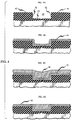
- Examples of such large oxide regions are the field oxide in MOS technology as well as the field oxide isolation region in bipolar technology. In the former case, typical configurations are shown in FIG. 1, where 10 and 11 are the respective drains of field effect transistors 8 and 9 , while 12 and 13 are the sources and 15 and 16 are the gates of these transistors.
- Interconnection between gates must be configured so that the electrical conductors producing these connections do not adversely affect device operation and such that the operation of one field effect transistor does not adversely interfere with the operation of another.
- a field oxide 17 This field oxide is usually thermally grown to a sufficient thickness--generally in the range 100 to 1000 nm--to prevent electric fields generated from runners that connect gates and junctions by traversing the region over the field oxide from producing a charge inverted region under the oxide. This inversion allows leakage currents to flow under the field oxide region between transistors.
- a large oxide is employed typically for the same reason.
- a photoresist deposited on a non-planar surface generally assumes substantially the same contour as that surface.
- images focused on the photoresist, although in focus at one point on the resist surface will be out of focus in the other regions of the resist surface that are not co-planar with the first.
- lithographic resolution is degraded.
- the isolation purposes of the dielectric are maintained while planarity and its associated benefits are obtained.
- a large area dielectric e.g., field oxide
- the surface of the field oxide should be no less than 20 nm above the surface of the silicon in which the active region is defined as shown in FIG. 2 and the dopant level in the silicon active region to a depth of at least ⁇ 100nm from the surface should be at least 10 17 atoms/cm 3 at the silicon/field oxide interface.
- a trench is formed in the active region.
- the surface of the trench is oxidized, a layer of polysilicon is deposited, field oxide is deposited over the polysilicon in the trench and then etched back to the desired geometric configuration.
- FIG. 1 is illustrative of typical configurations employed in the art
- FIGs. 2 and 3 are illustrative of configurations involved in the invention
- FIGs. 4 and 5 are illustrative of fabrication procedures involved in the invention.
- a trench-filled large area dielectric with a specific configuration allows production of an essentially planar region while avoiding stray capacitance or undesired depletion effects.
- trench-filled is not used to denote fabrication sequence but merely to indicate appearance after fabrication is complete.
- it is possible to form the device by building the field oxide region, and then surrounding it by an active region or by first etching a trench and filling the trench with the appropriate field oxide region.
- a trench field oxide is a field oxide having less oxide above the substrate surface than field oxide below this surface.
- a buried conducting region 30 between dielectric regions 34 and 35 is present.
- the conducting region generally should have a cross-section in the range 20 nm to 200 nm measured along the direction perpendicular to the trench sidewall at the midpoint between the lowest point of the trench and the upper major surface of the silicon. Regions thinner than 20 nm are difficult to produce without pin holes or voids, while regions thicker than 200 nm tend to undesirably increase capacitance to the gate runner and/or require a significantly deeper trench.
- the resistivity of the region should be less than 0.1 ohm-cm. Resistivities more than 0.1 ohm-cm lead to the possibility of transitory charge accumulation and poor contact to the substrate.
- the resistivity, when the conducting region is polysilicon, is generally adjusted by introducing n- or p-type dopants such as boron, arsenic, antimony and/or phosphorus. (N-type dopants are typically used over an N-tub and p-type dopants over a p-tub.) Typically dopant concentrations in the range 10 16 to 10 21 cm 3 yield the desired resistivity. The presence of the conducting region along the sidewall is significant.
- Presence of this region along the trench bottom has a less significant effect and is not essential because the field produced by the electrical conductors does not cause leakage between active devices when there is a conductor region at the sidewalls.
- presence of a conducting region along the trench bottom although often desirable, is not essential.
- the thickness of the oxide, 35 , between the buried conductive layer and the trench walls should typically be in the range 10 to 50 nm. Additionally, the top edge, 39 , of the conducting region 30 should preferably be oxidized to avoid shorting between the conducting region and the gate interconnect. If a buried conducting region is employed, the upper region 34 of the field oxide should be sufficiently thick to avoid excessive parasitic capacitance in the gate interconnect, e.g. should not contribute more than 10% to parasitic capacitance. In practice, the conductive region is electrically connected such as at 37 to the tub region so that the conducting layer is maintained at the tub potential.
- connection is made by techniques such as etching of the thin oxide between the tub and the conducting region using standard lithographic techniques followed by formation of the conductive layer including the interconnection. In a CMOS device this connection is made preferably to 1) the p tub or to 2) both the p tub and n tub. Additionally, if connection is made to both tubs the conducting region should be broken (shown in phantom at 90 in FIG. 3).
- a buried conductive region is not employed.
- the surface of dielectric in this embodiment should be carefully controlled.
- the surface 41 of the dielectric e.g., field oxide
- the dopant level in the silicon active region should be at least 10 17 atoms/cm 3 at the silicon/field oxide interface.
- the active region is any region containing an active device such as a capacitor, transistor, diode and resistor. Since substantial non-planarities are not desirable, it is advantageous to not substantially exceed the 20 nm step requirement.
- the dielectric region, 21 or 34 should have a thickness generally in the range 100 nm to 1000 nm. Thicknesses less than 100 nm lead to excessive capacitance, while thicknesses greater than 1000 nm lead to difficulties in maintaining planarity.
- Suitable materials for the dielectric region e.g., field oxide, are thermal oxides, spin-on oxides and deposited oxides such as chemical vapor deposited oxides.
- FIG. 4 A convenient procedure for producing the embodiment shown in FIG. 3 is illustrated in FIG. 4.
- a trench 40 is etched in the desired location.
- the trench is positioned between the active devices within a tub and/or positioned between tubs 43 and 44 .
- This objective is achieved in one embodiment by conventional photolithography or by depositing a dielectric, e.g. oxide or nitride, along the trench sidewalls over the conductor by a process described in Sze, supra, Chapter 11.
- This dielectric is then used as a mask for etching all of the conductor at the trench bottom or is used to convert the conductor through processes such as oxidation to an insulator.
- the photolithography mask used to etch openings in the conductor between tubs at the bottom of the field oxide need not be employed if a silicon region containing no active devices, surrounded by field oxide, and overlying the boundary region between p and n tubs is present. This silicon region is definable during the original trench etching. In this configuration the conductive region need not be present at the sidewalls of the silicon region having no active devices.
- the depth of the trench should be in the range 100 nm to 1000 nm. Trenches shallower than 100 nm lead to excessive capacitance while trenches deeper than 1000 nm are inconvenient to etch.
- a dielectric material is then formed on the exposed surfaces 52 and 53. Generally, this material is a dielectric, or combination of dielectrics, such as a thermal oxide, deposited oxide, or a deposited dielectric, e.g. silicon nitride formed as described in VLSI Technology, 2nd Edition, Edited by S. M. Sze, McGraw Hill, 1988, Chapter 3. Surface 43 and 44 should also be protected by a dielectric such as the same dielectric that is found on the surface 52 and 53 .
- the dielectric material, 48 is then deposited as shown in 4C.
- a convenient method for producing this dielectric is by using spin-on glasses as described in U.S. Patent Application Serial No. 161,876, filed February 29, 1988 (Smolinsky and Ryan which is hereby incorporated by reference). A sufficient thickness of dielectric should be deposited so that the surface in region 48 is higher than the surface of the polysilicon in region 45 .
- a sacrificial layer sufficiently thick to planarize the oxide layer is then deposited.
- This sacrificial layer is advantageously photoresist material.
- the photoresist material is then etched utilizing plasma-assisted procedures and plasma compositions such as described in Sze, supra, Chapter 5. Etching is continued until sufficient oxide is removed to yield the configuration shown in FIG. 4D.
- the exposed polysilicon over the active region is removed, for example, by conventional reactive ion etching while retaining the polysilicon along the sidewalls and bottom of the field oxide area.
- the edge of the exposed polysilicon region at the top of the sidewall is then passivated, for example, by thermal oxidation.
- the field oxide layer of thickness approximately equal to the trench depth is deposited, e.g. by means of chemical vapor deposition, and photoresist or other radiation definable material is deposited on the oxide layer.
- This material is then delineated by conventional techniques.
- the pattern of delineation is carefully chosen. In particular, the pattern is the negative of the trench mask and this negative pattern is reduced on all edges by a distance of at least the thickness of the deposited oxide. (If after this reduction, two edges are separated by less than the lithographically minimum resolvable dimension, they are eliminated from the defined pattern.)
- the unmasked oxide is etched until the underlying polysilicon is exposed in the area overlying the active region.
- the polysilicon acts as an etch stop for common etchants such as a chlorofluorocarbon based plasmas used to etch the oxide. Therefore, overetching is not a problem.
- the result of this oxide etch is the production of notches in the field oxide. These notches have tapered edges along the trench faces and nearly vertical edges defined by the mask edges. These notches are relatively small. The widths of the resulting notches, measured at their top, vary depending on trench dimension from a minimum width equal to the oxide thickness to a maximum width equal to the minimum resolvable dimension of the lithographic tool plus two oxide thicknesses.
- the widths at the top of the notches range from approximately 0.5 ⁇ m to approximately 2.0 ⁇ m.
- the widths at the bottom of the notches range from approximately zero to 1.0 ⁇ m.
- At least one edge of each notch is tapered. Therefore after removal of the masking material a second deposition of oxide easily fills these notches without leaving voids or producing a significant nonplanarity in the resulting surface. Etching of this surface therefore easily produces a planar field oxide even for extremely large area field oxide regions.
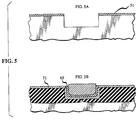
- the polysilicon layer overlying the active region once again acts as a convenient etch stop and as a protector of the active regions. It is possible to remove the exposed polysilicon layer and to process the then exposed active area to produce active devices and interconnects. The removal of the exposed polysilicon also results in a desirable extension of the field oxide region extending above the plane of the active area.
- an etch stop 51 such as silicon nitride (or silicon nitride over an oxide) is blanket deposited and simultaneously etched with the underlying silicon leaving the configuration shown in 5A.
- An oxide is then produced along the trench walls by thermal oxidation.
- a polysilicon region and the dielectric region are formed by deposition.
- the field oxide region and the exposed polysilicon are then etched back as shown in 5B to expose the nitride region 51 . It is possible to then remove and passivate the edge 65 of the polysilicon by means of selective polysilicon etching and subsequent oxidation. (Subsequent nitride removal is also possible.)
- This alternative procedure for producing a buried conductive region has the advantage of ensuring that the field oxide layer extends above the silicon surface and the conducting layer is protected by an oxide.
- another embodiment involves forming a continuous field oxide over the surface of the substrate, etching regions in this continuous field oxide for the active regions, forming the sidewall conducting regions, and then using selective epitaxial processes to form the active region of silicon in the previously etched areas.
- a buried conductive region in a planar large area oxide is also useful in bipolar technology to prevent inversion below field oxide regions.
- the procedure described for forming such a region is essentially the same as those discussed in conjunction with CMOS technology.
- a silicon substrate (major surface in the 100 crystallographic plane) was processed.
- a thermal oxide ⁇ 35nm in thickness was grown on both major surfaces of the substrate using an oxygen ambient and a temperature of approximately 900°C.
- a silicon nitride layer approximately ⁇ 200nm in thickness was deposited on the thermally grown oxides utilizing low pressure chemical vapor deposition including a SiH 2 Cl 2 + NH 3 gas flow.
- a thin layer of oxide was then formed on the nitride through thermal oxidation at 900°C in oxygen. Regions were opened in a positive acting, near ultraviolet resist spun onto the active side of the wafer. These openings were at locations where the field oxide ultimately was to be formed. The exposure and development of the resist was done by conventional lithographic techniques.
- the uncovered regions of the thin oxide and underlying nitride were then etched utilizing a conventional reactive ion etching procedure with the plasma gas including 10 sccm of Freon 23 (CHF 3 ) and 90 sccm of O 2 . Etching through the nitride took approximately 4.2 minutes and an overetch was employed to ensure complete clearing. After etching the resist was removed.
- the plasma gas including 10 sccm of Freon 23 (CHF 3 ) and 90 sccm of O 2 .
- trenches were etched into the silicon wafer.
- the trench etching was done utilizing a plasma gas including 85 sccm of CFCl 3 16 sccm of Cl 2 and 90 sccm of Ar.
- the etching was continued until a depth of ⁇ 500nm was reached.
- the exposed surfaces of the trench were then oxidized in steam at 900°C for 8 minutes. This oxidation produced an oxide layer approximately ⁇ 50nm in thickness.
- To produce a clean, undamaged surface the grown oxide was removed by immersing the wafer in a 30 to 1 aqueous HF solution.
- An oxide was again grown on the trench walls utilizing an oxygen ambient and a temperature of 900°C. The oxidation was continued until an oxide thickness of ⁇ 25nm was obtained.
- the grown oxide was then cleaned by immersing for 30 seconds in a 100 to 1 aqueous HF solution.
- ⁇ 100nm of polysilicon was deposited by utilizing a low pressure chemical vapor deposition technique with silane as the precursor gas.
- a ⁇ 20nm thick silicon dioxide layer was formed on the polysilicon surface by oxidizing in oxygen at 900°C.
- a ⁇ 500nm layer of undoped silicon dioxide was then deposited by subjecting the wafer at a temperature of 750°C to an atmosphere of tetraethoxysilane together with a dry N 2 flow. All the silicon dioxide, except on the sidewalls of the trench, was removed by subjecting the wafer to a reactive ion etching atmosphere including 75 sccm of CHF 3 and 12 sccm of O 2 for 12.5 min with a short overetch.
- the exposed regions of the polysilicon were removed utilizing a plasma struck in molecular chlorine. The etching was continued until the polysilicon was removed. To form the field oxide region, 1 ⁇ m of silicon dioxide was deposited utilizing the tetraethoxysilane low pressure chemical vapor deposition process previously described. The structure was then planarized by polishing using simultaneous mechanical and chemical polishing.
- Cross-sectional transmission electron microscopy of the resulting structure showed an essentially planar substrate having a buried field oxide and a conducting region separated from the trench sidewalls by a thin oxide.
Abstract
Description
- This invention relates to semiconductor devices and, in particular, semiconductor devices employing large area oxides such as field oxides.
- In a variety of electronic devices, relatively large areas, e.g. 20 to 90 percent of the device surface area of dielectric material, are employed to isolate one device active region from another and/or to prevent electric fields in one region from adversely affecting active devices in another region. Examples of such large oxide regions are the field oxide in MOS technology as well as the field oxide isolation region in bipolar technology. In the former case, typical configurations are shown in FIG. 1, where 10 and 11 are the respective drains of
field effect transistors - Interconnection between gates must be configured so that the electrical conductors producing these connections do not adversely affect device operation and such that the operation of one field effect transistor does not adversely interfere with the operation of another. Typically, these desires are satisfied by a
field oxide 17. This field oxide is usually thermally grown to a sufficient thickness--generally in the range 100 to 1000 nm--to prevent electric fields generated from runners that connect gates and junctions by traversing the region over the field oxide from producing a charge inverted region under the oxide. This inversion allows leakage currents to flow under the field oxide region between transistors. Similarly, in bipolar technology, a large oxide is employed typically for the same reason. - As design rules become stricter, i.e., as design rules decrease from 1 µm to .6 µm and finer, the large non-planarities associated with the large area dielectric regions produce significant processing difficulties. For example, a photoresist deposited on a non-planar surface generally assumes substantially the same contour as that surface. Thus, images focused on the photoresist, although in focus at one point on the resist surface, will be out of focus in the other regions of the resist surface that are not co-planar with the first. Thus, lithographic resolution is degraded.
- Additionally, when etching a non-planar surface, further difficulties occur. As gate material in
region 4 is etched and cleared, there remains a portion typically denominated a stringer, which must also be removed by further etching after the gate material has been removed fromsurfaces surfaces - Attempts have been made to limit non-planarities introduced by large area dielectrics through the thinning of the dielectric, e.g. oxide, employed. These attempts have yielded unsatisfactory results. In particular, with thin dielectrics, such as thin field oxides, electric fields produced in the overlying electrical runners strongly affect the silicon underlying the oxide. The result of this interaction is two-fold. Capacitance increases which yields a decrease in device speed. Additionally, voltages through the runner must be limited so that the
region 2 is not sufficiently inverted to produce substantial leakage currents, e.g., 10-7 to 10-9 amps betweendevices - By employing a large area dielectric, e.g., field oxide, formed in a trench that meets specific geometric requirements, the isolation purposes of the dielectric are maintained while planarity and its associated benefits are obtained. In particular, either buried conducting region(s), 30, that are essentially coextensive with the oxide sidewall should be formed as shown in FIG. 3, or in the absence of these region(s), the surface of the field oxide should be no less than 20 nm above the surface of the silicon in which the active region is defined as shown in FIG. 2 and the dopant level in the silicon active region to a depth of at least ø 100nm from the surface should be at least 1017 atoms/cm3 at the silicon/field oxide interface.
- Various methods are possible for producing the desired configuration. In one embodiment, a trench is formed in the active region. The surface of the trench is oxidized, a layer of polysilicon is deposited, field oxide is deposited over the polysilicon in the trench and then etched back to the desired geometric configuration.
- FIG. 1 is illustrative of typical configurations employed in the art; FIGs. 2 and 3 are illustrative of configurations involved in the invention; and FIGs. 4 and 5 are illustrative of fabrication procedures involved in the invention.
- As discussed, a trench-filled large area dielectric with a specific configuration allows production of an essentially planar region while avoiding stray capacitance or undesired depletion effects. (In the context of this invention the term trench-filled is not used to denote fabrication sequence but merely to indicate appearance after fabrication is complete. Thus, for example, it is possible to form the device by building the field oxide region, and then surrounding it by an active region or by first etching a trench and filling the trench with the appropriate field oxide region. Additionally, a trench field oxide is a field oxide having less oxide above the substrate surface than field oxide below this surface.) The particular geometries required are shown in FIGs. 2 and 3. The conducting region should be essentially coextensive with the sidewall. In FIG. 3 a buried conducting
region 30 betweendielectric regions range 20 nm to 200 nm measured along the direction perpendicular to the trench sidewall at the midpoint between the lowest point of the trench and the upper major surface of the silicon. Regions thinner than 20 nm are difficult to produce without pin holes or voids, while regions thicker than 200 nm tend to undesirably increase capacitance to the gate runner and/or require a significantly deeper trench. - Typically, the resistivity of the region should be less than 0.1 ohm-cm. Resistivities more than 0.1 ohm-cm lead to the possibility of transitory charge accumulation and poor contact to the substrate. The resistivity, when the conducting region is polysilicon, is generally adjusted by introducing n- or p-type dopants such as boron, arsenic, antimony and/or phosphorus. (N-type dopants are typically used over an N-tub and p-type dopants over a p-tub.) Typically dopant concentrations in the
range 1016 to 1021cm3 yield the desired resistivity. The presence of the conducting region along the sidewall is significant. Presence of this region along the trench bottom has a less significant effect and is not essential because the field produced by the electrical conductors does not cause leakage between active devices when there is a conductor region at the sidewalls. Thus, presence of a conducting region along the trench bottom, although often desirable, is not essential. - The thickness of the oxide, 35, between the buried conductive layer and the trench walls should typically be in the
range 10 to 50 nm. Additionally, the top edge, 39, of the conductingregion 30 should preferably be oxidized to avoid shorting between the conducting region and the gate interconnect. If a buried conducting region is employed, theupper region 34 of the field oxide should be sufficiently thick to avoid excessive parasitic capacitance in the gate interconnect, e.g. should not contribute more than 10% to parasitic capacitance. In practice, the conductive region is electrically connected such as at 37 to the tub region so that the conducting layer is maintained at the tub potential. This connection is made by techniques such as etching of the thin oxide between the tub and the conducting region using standard lithographic techniques followed by formation of the conductive layer including the interconnection. In a CMOS device this connection is made preferably to 1) the p tub or to 2) both the p tub and n tub. Additionally, if connection is made to both tubs the conducting region should be broken (shown in phantom at 90 in FIG. 3). - In the embodiment shown in FIG. 2 a buried conductive region is not employed. The surface of dielectric in this embodiment should be carefully controlled. To produce the desirable results associated with the invention, the
surface 41 of the dielectric, e.g., field oxide, should be no less than 20 nm above thesurface 22 of the active region and the dopant level in the silicon active region to a depth of at least ø 100nm from the surface should be at least 1017 atoms/cm3 at the silicon/field oxide interface. (Above, as used in this context, means measured from the silicon surface in the direction of the overlying oxide. The active region is any region containing an active device such as a capacitor, transistor, diode and resistor.) Since substantial non-planarities are not desirable, it is advantageous to not substantially exceed the 20 nm step requirement. - In either embodiment the dielectric region, 21 or 34, should have a thickness generally in the range 100 nm to 1000 nm. Thicknesses less than 100 nm lead to excessive capacitance, while thicknesses greater than 1000 nm lead to difficulties in maintaining planarity. Suitable materials for the dielectric region, e.g., field oxide, are thermal oxides, spin-on oxides and deposited oxides such as chemical vapor deposited oxides.
- A convenient procedure for producing the embodiment shown in FIG. 3 is illustrated in FIG. 4. In this procedure a
trench 40 is etched in the desired location. For CMOS applications, typically the trench is positioned between the active devices within a tub and/or positioned betweentubs Chapter 11. This dielectric is then used as a mask for etching all of the conductor at the trench bottom or is used to convert the conductor through processes such as oxidation to an insulator. The photolithography mask used to etch openings in the conductor between tubs at the bottom of the field oxide need not be employed if a silicon region containing no active devices, surrounded by field oxide, and overlying the boundary region between p and n tubs is present. This silicon region is definable during the original trench etching. In this configuration the conductive region need not be present at the sidewalls of the silicon region having no active devices. - Generally, the depth of the trench should be in the range 100 nm to 1000 nm. Trenches shallower than 100 nm lead to excessive capacitance while trenches deeper than 1000 nm are inconvenient to etch. A dielectric material is then formed on the exposed surfaces 52 and 53. Generally, this material is a dielectric, or combination of dielectrics, such as a thermal oxide, deposited oxide, or a deposited dielectric, e.g. silicon nitride formed as described in VLSI Technology, 2nd Edition, Edited by S. M. Sze, McGraw Hill, 1988, Chapter 3.
Surface surface - A layer of
polysilicon 45 as shown at 4B, having the thickness previously described, is then deposited onto the oxide. Suitable procedures for depositing the polysilicon are chemical vapor deposition and sputter deposition as described in Sze, supra, Chapter 6. It is also possible to electrically connect the buried conducting region to a tub region by a process such as described in U.S. Patent 4,825,278 dated April 25, 1989, which is hereby incorporated by reference. The dielectric material, 48, is then deposited as shown in 4C. A convenient method for producing this dielectric is by using spin-on glasses as described in U.S. Patent Application Serial No. 161,876, filed February 29, 1988 (Smolinsky and Ryan which is hereby incorporated by reference). A sufficient thickness of dielectric should be deposited so that the surface inregion 48 is higher than the surface of the polysilicon inregion 45. - To planarize closely spaced features, a sacrificial layer sufficiently thick to planarize the oxide layer is then deposited. This sacrificial layer is advantageously photoresist material. The photoresist material is then etched utilizing plasma-assisted procedures and plasma compositions such as described in Sze, supra, Chapter 5. Etching is continued until sufficient oxide is removed to yield the configuration shown in FIG. 4D. The exposed polysilicon over the active region is removed, for example, by conventional reactive ion etching while retaining the polysilicon along the sidewalls and bottom of the field oxide area. The edge of the exposed polysilicon region at the top of the sidewall is then passivated, for example, by thermal oxidation.
- In one advantageous approach to planarize widely spaced features, the field oxide layer of thickness approximately equal to the trench depth is deposited, e.g. by means of chemical vapor deposition, and photoresist or other radiation definable material is deposited on the oxide layer. This material is then delineated by conventional techniques. The pattern of delineation is carefully chosen. In particular, the pattern is the negative of the trench mask and this negative pattern is reduced on all edges by a distance of at least the thickness of the deposited oxide. (If after this reduction, two edges are separated by less than the lithographically minimum resolvable dimension, they are eliminated from the defined pattern.)
- After this delineation the unmasked oxide is etched until the underlying polysilicon is exposed in the area overlying the active region. (The polysilicon acts as an etch stop for common etchants such as a chlorofluorocarbon based plasmas used to etch the oxide. Therefore, overetching is not a problem.) The result of this oxide etch is the production of notches in the field oxide. These notches have tapered edges along the trench faces and nearly vertical edges defined by the mask edges. These notches are relatively small. The widths of the resulting notches, measured at their top, vary depending on trench dimension from a minimum width equal to the oxide thickness to a maximum width equal to the minimum resolvable dimension of the lithographic tool plus two oxide thicknesses. Typically, therefore, for an oxide thickness of 0.5 µm and a minimum resolvable dimension of 1 µm, the widths at the top of the notches range from approximately 0.5 µm to approximately 2.0 µm. The widths at the bottom of the notches range from approximately zero to 1.0 µm. At least one edge of each notch is tapered. Therefore after removal of the masking material a second deposition of oxide easily fills these notches without leaving voids or producing a significant nonplanarity in the resulting surface. Etching of this surface therefore easily produces a planar field oxide even for extremely large area field oxide regions. The polysilicon layer overlying the active region once again acts as a convenient etch stop and as a protector of the active regions. It is possible to remove the exposed polysilicon layer and to process the then exposed active area to produce active devices and interconnects. The removal of the exposed polysilicon also results in a desirable extension of the field oxide region extending above the plane of the active area.
- In an alternative procedure, before etching to obtain the configuration shown in FIG. 4A, an
etch stop 51 such as silicon nitride (or silicon nitride over an oxide) is blanket deposited and simultaneously etched with the underlying silicon leaving the configuration shown in 5A. An oxide is then produced along the trench walls by thermal oxidation. Subsequently, a polysilicon region and the dielectric region are formed by deposition. The field oxide region and the exposed polysilicon are then etched back as shown in 5B to expose thenitride region 51. It is possible to then remove and passivate theedge 65 of the polysilicon by means of selective polysilicon etching and subsequent oxidation. (Subsequent nitride removal is also possible.) This alternative procedure for producing a buried conductive region has the advantage of ensuring that the field oxide layer extends above the silicon surface and the conducting layer is protected by an oxide. - As previously discussed, another embodiment involves forming a continuous field oxide over the surface of the substrate, etching regions in this continuous field oxide for the active regions, forming the sidewall conducting regions, and then using selective epitaxial processes to form the active region of silicon in the previously etched areas.
- To produce the configuration of the second embodiment shown in FIG. 2, a similar procedure is utilized, except a deposition of a conductive polysilicon layer is omitted. Subsequent processing to produce the desired device is well-known. Examples of this processing are described in reviews such as Sze, supra,
Chapter 11. - The use of a buried conductive region in a planar large area oxide is also useful in bipolar technology to prevent inversion below field oxide regions. The procedure described for forming such a region is essentially the same as those discussed in conjunction with CMOS technology.
- The following example is illustrative of of procedures involved in the invention.
- A silicon substrate (major surface in the 100 crystallographic plane) was processed. A thermal oxide ø 35nm in thickness was grown on both major surfaces of the substrate using an oxygen ambient and a temperature of approximately 900°C. A silicon nitride layer approximately ø 200nm in thickness was deposited on the thermally grown oxides utilizing low pressure chemical vapor deposition including a SiH2Cl2 + NH3 gas flow. A thin layer of oxide was then formed on the nitride through thermal oxidation at 900°C in oxygen. Regions were opened in a positive acting, near ultraviolet resist spun onto the active side of the wafer. These openings were at locations where the field oxide ultimately was to be formed. The exposure and development of the resist was done by conventional lithographic techniques. The uncovered regions of the thin oxide and underlying nitride were then etched utilizing a conventional reactive ion etching procedure with the plasma gas including 10 sccm of Freon 23 (CHF3) and 90 sccm of O2. Etching through the nitride took approximately 4.2 minutes and an overetch was employed to ensure complete clearing. After etching the resist was removed.
- Using the patterned silicon nitride as a mask, trenches were etched into the silicon wafer. The trench etching was done utilizing a plasma gas including 85 sccm of
CFCl 3 16 sccm of Cl2 and 90 sccm of Ar. The etching was continued until a depth of ø 500nm was reached. The exposed surfaces of the trench were then oxidized in steam at 900°C for 8 minutes. This oxidation produced an oxide layer approximately ø 50nm in thickness. To produce a clean, undamaged surface the grown oxide was removed by immersing the wafer in a 30 to 1 aqueous HF solution. An oxide was again grown on the trench walls utilizing an oxygen ambient and a temperature of 900°C. The oxidation was continued until an oxide thickness of ø 25nm was obtained. The grown oxide was then cleaned by immersing for 30 seconds in a 100 to 1 aqueous HF solution. - Immediately after cleaning, ø 100nm of polysilicon was deposited by utilizing a low pressure chemical vapor deposition technique with silane as the precursor gas. A ø 20nm thick silicon dioxide layer was formed on the polysilicon surface by oxidizing in oxygen at 900°C. A ø 500nm layer of undoped silicon dioxide was then deposited by subjecting the wafer at a temperature of 750°C to an atmosphere of tetraethoxysilane together with a dry N2 flow. All the silicon dioxide, except on the sidewalls of the trench, was removed by subjecting the wafer to a reactive ion etching atmosphere including 75 sccm of CHF3 and 12 sccm of O2 for 12.5 min with a short overetch. Utilizing the remaining silicon dioxide as a mask, the exposed regions of the polysilicon were removed utilizing a plasma struck in molecular chlorine. The etching was continued until the polysilicon was removed. To form the field oxide region, 1 µm of silicon dioxide was deposited utilizing the tetraethoxysilane low pressure chemical vapor deposition process previously described. The structure was then planarized by polishing using simultaneous mechanical and chemical polishing.
- Cross-sectional transmission electron microscopy of the resulting structure showed an essentially planar substrate having a buried field oxide and a conducting region separated from the trench sidewalls by a thin oxide.
Claims (6)
- A device comprising 1) a substrate, 2) first and second active regions comprising silicon, 3) a region of dielectric material, said dielectric material positioned within said device to limit interaction of charge or electric field through said substrate and 4) transistors in said first and second active regions, said transistors comprising a gate, source, and drain
characterised in thatsaid dielectric material occupies a trench between said first and second active region,the surface of said region of dielectric material extends at least 20 nm above the plane of the surface of the said active region, directly underneath the position where said gate crosses said dielectric material, andthe dopant level in said silicon active regions to the depth of 100 nm from the surface of said active region at the silicon/field oxide interface is at least 1017 atoms/cm3. - The device of claim 1 wherein said device comprises an integrated circuit including field effect transistors in said active regions.
- The device of claim 1 wherein said device comprises an integrated circuit including bipolar transistors in said active regions.
- The device of claim 1 wherein said dielectric material comprises a silicon oxide.
- The device of claim 4 wherein said conductive region comprises silicon.
- The device of claim 1 wherein said conductive region comprises silicon.
Applications Claiming Priority (3)
| Application Number | Priority Date | Filing Date | Title |
|---|---|---|---|
| US38747889A | 1989-07-28 | 1989-07-28 | |
| US387478 | 1989-07-28 | ||
| EP90307846A EP0410633B1 (en) | 1989-07-28 | 1990-07-18 | Planar isolation technique for integrated circuits |
Related Parent Applications (1)
| Application Number | Title | Priority Date | Filing Date |
|---|---|---|---|
| EP90307846A Division EP0410633B1 (en) | 1989-07-28 | 1990-07-18 | Planar isolation technique for integrated circuits |
Publications (3)
| Publication Number | Publication Date |
|---|---|
| EP1143505A2 true EP1143505A2 (en) | 2001-10-10 |
| EP1143505A3 EP1143505A3 (en) | 2001-11-07 |
| EP1143505B1 EP1143505B1 (en) | 2006-09-13 |
Family
ID=23530045
Family Applications (2)
| Application Number | Title | Priority Date | Filing Date |
|---|---|---|---|
| EP90307846A Expired - Lifetime EP0410633B1 (en) | 1989-07-28 | 1990-07-18 | Planar isolation technique for integrated circuits |
| EP01202722A Expired - Lifetime EP1143505B1 (en) | 1989-07-28 | 1990-07-18 | Planar isolation technique for integrated circuits |
Family Applications Before (1)
| Application Number | Title | Priority Date | Filing Date |
|---|---|---|---|
| EP90307846A Expired - Lifetime EP0410633B1 (en) | 1989-07-28 | 1990-07-18 | Planar isolation technique for integrated circuits |
Country Status (6)
| Country | Link |
|---|---|
| US (1) | US5373180A (en) |
| EP (2) | EP0410633B1 (en) |
| JP (1) | JPH0366145A (en) |
| KR (1) | KR940004995B1 (en) |
| CA (1) | CA2016449C (en) |
| DE (2) | DE69034048T2 (en) |
Families Citing this family (5)
| Publication number | Priority date | Publication date | Assignee | Title |
|---|---|---|---|---|
| WO1996002070A2 (en) * | 1994-07-12 | 1996-01-25 | National Semiconductor Corporation | Integrated circuit comprising a trench isolation structure and an oxygen barrier layer and method for forming the integrated circuit |
| JP3904676B2 (en) | 1997-04-11 | 2007-04-11 | 株式会社ルネサステクノロジ | Method for manufacturing trench type element isolation structure and trench type element isolation structure |
| US6472335B1 (en) * | 1998-10-19 | 2002-10-29 | Taiwan Semiconductor Manufacturing Company | Methods of adhesion promoter between low-K layer and underlying insulating layer |
| JP2004172310A (en) * | 2002-11-19 | 2004-06-17 | Renesas Technology Corp | Method for manufacturing semiconductor device |
| KR100618698B1 (en) * | 2004-06-21 | 2006-09-08 | 주식회사 하이닉스반도체 | Semiconductor device and method of manufacturing the same |
Citations (6)
| Publication number | Priority date | Publication date | Assignee | Title |
|---|---|---|---|---|
| JPS598353A (en) * | 1982-07-07 | 1984-01-17 | Nec Corp | Semiconductor integrated circuit device |
| US4571819A (en) * | 1984-11-01 | 1986-02-25 | Ncr Corporation | Method for forming trench isolation structures |
| EP0220392A2 (en) * | 1985-10-30 | 1987-05-06 | International Business Machines Corporation | A trench-incorporated monolithic semiconductor capacitor and high density dynamic memory cells including the capacitor |
| EP0287931A2 (en) * | 1987-04-14 | 1988-10-26 | Kabushiki Kaisha Toshiba | Semiconductor device comprising an electrode having a composite structure |
| US4825278A (en) * | 1985-10-17 | 1989-04-25 | American Telephone And Telegraph Company At&T Bell Laboratories | Radiation hardened semiconductor devices |
| EP0316165A2 (en) * | 1987-11-11 | 1989-05-17 | Seiko Instruments Inc. | A method of trench isolation |
Family Cites Families (5)
| Publication number | Priority date | Publication date | Assignee | Title |
|---|---|---|---|---|
| JPS59217339A (en) * | 1983-05-26 | 1984-12-07 | Toshiba Corp | Manufacture of semiconductor device |
| JPS6132544A (en) * | 1984-07-25 | 1986-02-15 | Matsushita Electric Ind Co Ltd | Manufacture of semiconductor integrated circuit device |
| JPS61271854A (en) * | 1985-05-27 | 1986-12-02 | Nec Corp | Semiconductor-element isolating structure and manufacture thereof |
| JPH01138730A (en) * | 1987-11-25 | 1989-05-31 | Fujitsu Ltd | Semiconductor device |
| JPH0797627B2 (en) * | 1987-12-21 | 1995-10-18 | 株式会社日立製作所 | Semiconductor device |
-
1990
- 1990-05-10 CA CA002016449A patent/CA2016449C/en not_active Expired - Lifetime
- 1990-07-18 DE DE69034048T patent/DE69034048T2/en not_active Expired - Lifetime
- 1990-07-18 EP EP90307846A patent/EP0410633B1/en not_active Expired - Lifetime
- 1990-07-18 DE DE69034230T patent/DE69034230T2/en not_active Expired - Lifetime
- 1990-07-18 EP EP01202722A patent/EP1143505B1/en not_active Expired - Lifetime
- 1990-07-25 KR KR1019900011298A patent/KR940004995B1/en not_active IP Right Cessation
- 1990-07-27 JP JP2201056A patent/JPH0366145A/en active Pending
-
1993
- 1993-09-14 US US08/121,082 patent/US5373180A/en not_active Expired - Lifetime
Patent Citations (6)
| Publication number | Priority date | Publication date | Assignee | Title |
|---|---|---|---|---|
| JPS598353A (en) * | 1982-07-07 | 1984-01-17 | Nec Corp | Semiconductor integrated circuit device |
| US4571819A (en) * | 1984-11-01 | 1986-02-25 | Ncr Corporation | Method for forming trench isolation structures |
| US4825278A (en) * | 1985-10-17 | 1989-04-25 | American Telephone And Telegraph Company At&T Bell Laboratories | Radiation hardened semiconductor devices |
| EP0220392A2 (en) * | 1985-10-30 | 1987-05-06 | International Business Machines Corporation | A trench-incorporated monolithic semiconductor capacitor and high density dynamic memory cells including the capacitor |
| EP0287931A2 (en) * | 1987-04-14 | 1988-10-26 | Kabushiki Kaisha Toshiba | Semiconductor device comprising an electrode having a composite structure |
| EP0316165A2 (en) * | 1987-11-11 | 1989-05-17 | Seiko Instruments Inc. | A method of trench isolation |
Non-Patent Citations (3)
| Title |
|---|
| PATENT ABSTRACTS OF JAPAN vol. 008, no. 088 (E-240), 21 April 1984 (1984-04-21) & JP 59 008353 A (NIPPON DENKI KK), 17 January 1984 (1984-01-17) * |
| SZE S.M: 'VLSI TECHNOLOGY', 1984, MCGRAW-HILL, SINGAPORE * |
| W.P. DUMKE: "Bipolar isolation technique" IBM TECHNICAL DISCLOSURE BULLETIN, vol. 22, no. 7, December 1979 (1979-12), pages 2946-2947, XP002177346 * |
Also Published As
| Publication number | Publication date |
|---|---|
| DE69034230D1 (en) | 2006-10-26 |
| EP1143505B1 (en) | 2006-09-13 |
| EP1143505A3 (en) | 2001-11-07 |
| CA2016449C (en) | 1996-06-25 |
| JPH0366145A (en) | 1991-03-20 |
| EP0410633A2 (en) | 1991-01-30 |
| KR910003782A (en) | 1991-02-28 |
| EP0410633B1 (en) | 2003-03-12 |
| KR940004995B1 (en) | 1994-06-09 |
| US5373180A (en) | 1994-12-13 |
| DE69034230T2 (en) | 2007-09-13 |
| DE69034048D1 (en) | 2003-04-17 |
| DE69034048T2 (en) | 2003-12-24 |
| CA2016449A1 (en) | 1991-01-28 |
| EP0410633A3 (en) | 1991-02-27 |
Similar Documents
| Publication | Publication Date | Title |
|---|---|---|
| US6033980A (en) | Method of forming submicron contacts and vias in an integrated circuit | |
| US5915195A (en) | Ion implantation process to improve the gate oxide quality at the edge of a shallow trench isolation structure | |
| US5516710A (en) | Method of forming a transistor | |
| EP0166983A2 (en) | Method of selectively exposing the sidewalls of a trench and its use to the forming of a metal silicide substrate contact for dielectric filled deep trench isolated devices | |
| US6828205B2 (en) | Method using wet etching to trim a critical dimension | |
| US4563227A (en) | Method for manufacturing a semiconductor device | |
| US4419813A (en) | Method for fabricating semiconductor device | |
| US3943542A (en) | High reliability, low leakage, self-aligned silicon gate FET and method of fabricating same | |
| US5930620A (en) | Resistance to gate dielectric breakdown at the edges of shallow trench isolation structures | |
| US6180517B1 (en) | Method of forming submicron contacts and vias in an integrated circuit | |
| EP0600149B1 (en) | Method of making a self aligned static induction transistor | |
| US6579801B1 (en) | Method for enhancing shallow trench top corner rounding using endpoint control of nitride layer etch process with appropriate etch front | |
| EP0526244B1 (en) | Method of forming a polysilicon buried contact | |
| US5373180A (en) | Planar isolation technique for integrated circuits | |
| US6399432B1 (en) | Process to control poly silicon profiles in a dual doped poly silicon process | |
| JP3407023B2 (en) | Method for manufacturing semiconductor device | |
| US5449627A (en) | Lateral bipolar transistor and FET compatible process for making it | |
| EP0239384B1 (en) | Process for isolating semiconductor devices on a substrate | |
| US6235609B1 (en) | Method for forming isolation areas with improved isolation oxide | |
| US5998302A (en) | Method of manufacturing semiconductor device | |
| US6040233A (en) | Method of making a shallow trench isolation with thin nitride as gate dielectric | |
| US6383937B1 (en) | Method of fabricating a silicon island | |
| US6417033B1 (en) | Method of fabricating a silicon island | |
| US20230060695A1 (en) | Deep trench isolation with field oxide | |
| KR940004252B1 (en) | Isolation method with local polyoxide |
Legal Events
| Date | Code | Title | Description |
|---|---|---|---|
| PUAI | Public reference made under article 153(3) epc to a published international application that has entered the european phase |
Free format text: ORIGINAL CODE: 0009012 |
|
| PUAL | Search report despatched |
Free format text: ORIGINAL CODE: 0009013 |
|
| 17P | Request for examination filed |
Effective date: 20010717 |
|
| AC | Divisional application: reference to earlier application |
Ref document number: 410633 Country of ref document: EP |
|
| AK | Designated contracting states |
Kind code of ref document: A2 Designated state(s): DE FR GB NL |
|
| AK | Designated contracting states |
Kind code of ref document: A3 Designated state(s): DE FR GB NL |
|
| RIC1 | Information provided on ipc code assigned before grant |
Free format text: 7H 01L 21/76 A, 7H 01L 21/762 B |
|
| RIN1 | Information on inventor provided before grant (corrected) |
Inventor name: MANCHANDA, LALITA Inventor name: HILLENIUS, STEVEN J. Inventor name: VAIDYA, SHIELA Inventor name: LYNCH, WILLIAM THOMAS Inventor name: PINTO, MARK RICHARD |
|
| AKX | Designation fees paid |
Free format text: DE FR GB NL |
|
| 17Q | First examination report despatched |
Effective date: 20040225 |
|
| GRAP | Despatch of communication of intention to grant a patent |
Free format text: ORIGINAL CODE: EPIDOSNIGR1 |
|
| GRAS | Grant fee paid |
Free format text: ORIGINAL CODE: EPIDOSNIGR3 |
|
| GRAA | (expected) grant |
Free format text: ORIGINAL CODE: 0009210 |
|
| AC | Divisional application: reference to earlier application |
Ref document number: 0410633 Country of ref document: EP Kind code of ref document: P |
|
| AK | Designated contracting states |
Kind code of ref document: B1 Designated state(s): DE FR GB NL |
|
| PG25 | Lapsed in a contracting state [announced via postgrant information from national office to epo] |
Ref country code: NL Free format text: LAPSE BECAUSE OF FAILURE TO SUBMIT A TRANSLATION OF THE DESCRIPTION OR TO PAY THE FEE WITHIN THE PRESCRIBED TIME-LIMIT Effective date: 20060913 |
|
| REG | Reference to a national code |
Ref country code: GB Ref legal event code: FG4D |
|
| REF | Corresponds to: |
Ref document number: 69034230 Country of ref document: DE Date of ref document: 20061026 Kind code of ref document: P |
|
| NLV1 | Nl: lapsed or annulled due to failure to fulfill the requirements of art. 29p and 29m of the patents act | ||
| ET | Fr: translation filed | ||
| PLBE | No opposition filed within time limit |
Free format text: ORIGINAL CODE: 0009261 |
|
| STAA | Information on the status of an ep patent application or granted ep patent |
Free format text: STATUS: NO OPPOSITION FILED WITHIN TIME LIMIT |
|
| 26N | No opposition filed |
Effective date: 20070614 |
|
| PGFP | Annual fee paid to national office [announced via postgrant information from national office to epo] |
Ref country code: FR Payment date: 20090716 Year of fee payment: 20 |
|
| PGFP | Annual fee paid to national office [announced via postgrant information from national office to epo] |
Ref country code: GB Payment date: 20090720 Year of fee payment: 20 Ref country code: DE Payment date: 20090722 Year of fee payment: 20 |
|
| REG | Reference to a national code |
Ref country code: GB Ref legal event code: PE20 Expiry date: 20100717 |
|
| PG25 | Lapsed in a contracting state [announced via postgrant information from national office to epo] |
Ref country code: GB Free format text: LAPSE BECAUSE OF EXPIRATION OF PROTECTION Effective date: 20100717 |
|
| PG25 | Lapsed in a contracting state [announced via postgrant information from national office to epo] |
Ref country code: DE Free format text: LAPSE BECAUSE OF EXPIRATION OF PROTECTION Effective date: 20100718 |