EP1143300A1 - Photoresist compositions and use of same - Google Patents

Photoresist compositions and use of same Download PDF

Info

Publication number
EP1143300A1
EP1143300A1 EP01303145A EP01303145A EP1143300A1 EP 1143300 A1 EP1143300 A1 EP 1143300A1 EP 01303145 A EP01303145 A EP 01303145A EP 01303145 A EP01303145 A EP 01303145A EP 1143300 A1 EP1143300 A1 EP 1143300A1
Authority
EP
European Patent Office
Prior art keywords
photoresist
groups
development
crosslinking
component
Prior art date
Legal status (The legal status is an assumption and is not a legal conclusion. Google has not performed a legal analysis and makes no representation as to the accuracy of the status listed.)
Withdrawn
Application number
EP01303145A
Other languages
German (de)
French (fr)
Inventor
Timothy G. Adams
Current Assignee (The listed assignees may be inaccurate. Google has not performed a legal analysis and makes no representation or warranty as to the accuracy of the list.)
Rohm and Haas Electronic Materials LLC
Original Assignee
Shipley Co LLC
Priority date (The priority date is an assumption and is not a legal conclusion. Google has not performed a legal analysis and makes no representation as to the accuracy of the date listed.)
Filing date
Publication date
Application filed by Shipley Co LLC filed Critical Shipley Co LLC
Publication of EP1143300A1 publication Critical patent/EP1143300A1/en
Withdrawn legal-status Critical Current

Links

Classifications

    • GPHYSICS
    • G03PHOTOGRAPHY; CINEMATOGRAPHY; ANALOGOUS TECHNIQUES USING WAVES OTHER THAN OPTICAL WAVES; ELECTROGRAPHY; HOLOGRAPHY
    • G03FPHOTOMECHANICAL PRODUCTION OF TEXTURED OR PATTERNED SURFACES, e.g. FOR PRINTING, FOR PROCESSING OF SEMICONDUCTOR DEVICES; MATERIALS THEREFOR; ORIGINALS THEREFOR; APPARATUS SPECIALLY ADAPTED THEREFOR
    • G03F7/00Photomechanical, e.g. photolithographic, production of textured or patterned surfaces, e.g. printing surfaces; Materials therefor, e.g. comprising photoresists; Apparatus specially adapted therefor
    • G03F7/004Photosensitive materials
    • G03F7/027Non-macromolecular photopolymerisable compounds having carbon-to-carbon double bonds, e.g. ethylenic compounds
    • G03F7/028Non-macromolecular photopolymerisable compounds having carbon-to-carbon double bonds, e.g. ethylenic compounds with photosensitivity-increasing substances, e.g. photoinitiators
    • GPHYSICS
    • G03PHOTOGRAPHY; CINEMATOGRAPHY; ANALOGOUS TECHNIQUES USING WAVES OTHER THAN OPTICAL WAVES; ELECTROGRAPHY; HOLOGRAPHY
    • G03FPHOTOMECHANICAL PRODUCTION OF TEXTURED OR PATTERNED SURFACES, e.g. FOR PRINTING, FOR PROCESSING OF SEMICONDUCTOR DEVICES; MATERIALS THEREFOR; ORIGINALS THEREFOR; APPARATUS SPECIALLY ADAPTED THEREFOR
    • G03F7/00Photomechanical, e.g. photolithographic, production of textured or patterned surfaces, e.g. printing surfaces; Materials therefor, e.g. comprising photoresists; Apparatus specially adapted therefor
    • G03F7/004Photosensitive materials
    • G03F7/039Macromolecular compounds which are photodegradable, e.g. positive electron resists
    • G03F7/0392Macromolecular compounds which are photodegradable, e.g. positive electron resists the macromolecular compound being present in a chemically amplified positive photoresist composition
    • GPHYSICS
    • G03PHOTOGRAPHY; CINEMATOGRAPHY; ANALOGOUS TECHNIQUES USING WAVES OTHER THAN OPTICAL WAVES; ELECTROGRAPHY; HOLOGRAPHY
    • G03FPHOTOMECHANICAL PRODUCTION OF TEXTURED OR PATTERNED SURFACES, e.g. FOR PRINTING, FOR PROCESSING OF SEMICONDUCTOR DEVICES; MATERIALS THEREFOR; ORIGINALS THEREFOR; APPARATUS SPECIALLY ADAPTED THEREFOR
    • G03F7/00Photomechanical, e.g. photolithographic, production of textured or patterned surfaces, e.g. printing surfaces; Materials therefor, e.g. comprising photoresists; Apparatus specially adapted therefor
    • G03F7/26Processing photosensitive materials; Apparatus therefor
    • G03F7/40Treatment after imagewise removal, e.g. baking
    • GPHYSICS
    • G03PHOTOGRAPHY; CINEMATOGRAPHY; ANALOGOUS TECHNIQUES USING WAVES OTHER THAN OPTICAL WAVES; ELECTROGRAPHY; HOLOGRAPHY
    • G03FPHOTOMECHANICAL PRODUCTION OF TEXTURED OR PATTERNED SURFACES, e.g. FOR PRINTING, FOR PROCESSING OF SEMICONDUCTOR DEVICES; MATERIALS THEREFOR; ORIGINALS THEREFOR; APPARATUS SPECIALLY ADAPTED THEREFOR
    • G03F7/00Photomechanical, e.g. photolithographic, production of textured or patterned surfaces, e.g. printing surfaces; Materials therefor, e.g. comprising photoresists; Apparatus specially adapted therefor
    • G03F7/004Photosensitive materials
    • G03F7/0045Photosensitive materials with organic non-macromolecular light-sensitive compounds not otherwise provided for, e.g. dissolution inhibitors
    • YGENERAL TAGGING OF NEW TECHNOLOGICAL DEVELOPMENTS; GENERAL TAGGING OF CROSS-SECTIONAL TECHNOLOGIES SPANNING OVER SEVERAL SECTIONS OF THE IPC; TECHNICAL SUBJECTS COVERED BY FORMER USPC CROSS-REFERENCE ART COLLECTIONS [XRACs] AND DIGESTS
    • Y10TECHNICAL SUBJECTS COVERED BY FORMER USPC
    • Y10STECHNICAL SUBJECTS COVERED BY FORMER USPC CROSS-REFERENCE ART COLLECTIONS [XRACs] AND DIGESTS
    • Y10S430/00Radiation imagery chemistry: process, composition, or product thereof
    • Y10S430/1053Imaging affecting physical property or radiation sensitive material, or producing nonplanar or printing surface - process, composition, or product: radiation sensitive composition or product or process of making binder containing
    • Y10S430/1055Radiation sensitive composition or product or process of making
    • Y10S430/106Binder containing
    • Y10S430/111Polymer of unsaturated acid or ester

Definitions

  • the present invention relates to new photoresists, particularly photoresists that can crosslink after a development step, typically through thermal treatment. Resists of the invention are particularly useful to provide thermal flow coverage of semiconductor contact holes.
  • Photoresists arc photosensitive films used for transfer of images to a substrate.
  • a coating layer of a photoresist is formed on a substrate and the photoresist layer is then exposed through a photomask to a source of activating radiation.
  • the photomask has areas that are opaque to activating radiation and other areas that are transparent to activating radiation. Exposure to activating radiation provides a photoinduced chemical transformation of the photoresist coating to thereby transfer the pattern of the photomask to the photoresist coated substrate.
  • the photoresist is developed to provide a relief image that permits selective processing of a substrate.
  • a photoresist can be either positive-acting or negative-acting.
  • those coating layer portions that are exposed to activating radiation polymerize or crosslink in a reaction between a photoactive compound and polymerizable reagents of the photoresist composition. Consequently, the exposed coating portions are rendered less soluble in a developer solution than unexposed portions.
  • exposed portions are rendered more soluble in a developer solution while areas not exposed remain comparatively less developer soluble.
  • Chemically-amplified-type resists have been increasingly employed, particularly for formation of sub-micron images and other high performance applications.
  • Such photoresists may be negative-acting or positive-acting and generally include many crosslinking events (in the case of a negative-acting resist) or deprotection reactions (in the case of a positive-acting resist) per unit of photogenerated acid.
  • certain cationic photo-initiators have been used to induce cleavage of certain "blocking" groups pendant from a photorcsist binder, or cleavage of certain groups that comprise a photoresist binder backbone. See, for example, U.S. Patents Nos.
  • a polar functional group is formed, e.g., carboxyl or imide, which results in different solubility characteristics in exposed and unexposed areas of the resist coating layer. See also R.D. Allen et al., Proceedings of SPIE , 2724:334-343 (1996); and P, Trefonas et al. Proceedings of the 11 th International Conference on Photopolymers (Soc. Of Plastics Engineers), pp 44-58 (Oct. 6, 1997).
  • Microelectronic devices frequently have multiple metal interconnection or conductive layers that are each separated by interposed insulating (dielectric) layers.
  • the multiple conductive layers are connected using contact hole or via holes through the dielectric layers. See, generally, S. Sze, VLSI Technology (2 nd ed., New York, McGraw-Hill, 1988), for a discussion of semiconductor device fabrication techniques.
  • compositions and methods of the invention provide for a controlled flow of resist into device contact (via) holes during a post-exposure, post-development hard-bake step.
  • Resists of the invention are positive-acting and contain one or more components that are preferably substantially stable (i.e. no substantial crosslinking) during: 1) soft-bake, pre-exposure thermal treatment to remove solvent carrier of the applied resist, and 2) post-exposure, pre-development thermal treatment to promote or enhance the acid-promoted reaction in exposed regions (typically a de-blocking reaction).
  • resists of the invention will crosslink during a post-development more stringent thermal treatment (thermal flow hard-bake step). By such selective crosslinking, the thermal flow rate of the applied resist into the contact holes can be controlled to within a desired range.
  • the hard bake e.g. at least about 120°C, more typically at least about 130°C or 140°C, suitably from about 130°C to about 140°C to about 180°C or about 190°C
  • the hard bake can produce too fast of a flow rate, which can limit resolution of formed features.
  • One preferred resist for use in accordance with the invention contains a photoactive component (typically a photoacid generator) and a resin with acetal and/or ketal moieties.
  • acetal as used herein is inclusive of both acetal and ketal moieties, unless Otherwise indicated.
  • the resin can crosslink, typically by a transacetalation reaction. The hard-bake thermal treatment will cause flow of the resist as desired into a contact hole feature over which the resist has been applied, while the resist crosslinking will restrict the resist flow rate to a desired rate.
  • the resist resin typically is above its Tg.
  • Suitable resist components that contain acetal groups that will react (crosslink) during a post-development hard-bake can be provided by a variety of routes.
  • a vinyl ether e.g. t-butyl vinyl ether
  • a hydroxy moiety such as phenolic -OH group
  • a polymer or copolymer containing phenolic units such as a poly(vinylphenol) polymer or compolymer
  • a vinyl ether can be reacted with a vinyl ether to provide the thermally reactive acetal moieties.
  • resists can be employed in accordance with the invention provided one or more components of the resist can undergo crosslinking during a stringent hardbake step, but remain substantially stable (i.e. no substantial crosslinking) during prior thermal processing (i.e. pre-exposure soft bake and post-exposure, pre-development bake).
  • resists can employed that contain a resin that can contains ester groups (e.g. t-butyl ester groups) that can undergo crosslinking, such as by a transacetalation reaction.
  • Resists of the invention will typically contain separate components or functionalities that will be photoacid-labile arid will be reactive upon exposure and any post-exposure, pre-development thermal treatment.
  • Preferred photoacid-labile groups include acetal groups that are more reactive to photoacid-induced deblocking than the moieties that will crosslink during a post-development, hard-bake step.
  • a resist resin can be employed that has both primary or second acetal groups and a tertiary acetal, or a primary acetal and a second or tertiary acetal.
  • the more branched acetal i.e.
  • Resists of the invention also may contain a thermal acid generator, which is substantially stable to temperatures of a soft-bake step or a post-exposure, pre-development heat treatment, but can be activated to generate acid during more stringent temperatures of a post-development hard-bake step.
  • the thermally generated acid then can promote crosslinking between resist component(s).
  • use of a thermal acid generator will be less preferred to avoid degradation of the resist during storage prior to use.
  • Resins used in resists of the invention can include a variety of units, including aromatic groups e.g. phenolic groups; cyano groups such as provide by polymerization of acrylonitrile or methacrylonitrile; and the like.
  • Polymers of the invention also may be substantially, essentially or completely free of phenyl or other aromatic groups, particularly for short wavelength imaging applications, such as 193 nm, 157 nm and other sub-200 nm wavelength exposures where aromatic groups can absorb excessive exposure radiation.
  • aromatic groups can absorb excessive exposure radiation.
  • polymers Preferably such polymers have less than about 5 mole percent aromatic groups, based on the total polymer, more preferably less than about 3, 2, 1, 0,5, or 0.1 mole percent aromatic groups.
  • Particularly preferred polymers for such wavelength imaging will be completely free of aromatic groups.
  • crosslinking or other similar term are intended to refer to essentially any covalent linkage between polymer chains or sites.
  • references herein that a polymer or other component "does not undergo substantial crosslinking" or other similar phrase indicates that less than 20 mole percent of crosslinkable groups (i.e. crosslinkable upon subsequent more stringent post-development hard-bake) of the crosslinkable polymer or other component do not react upon exposure to a stated temperature for 60 seconds.
  • references herein that a polymer does not substantially crosslink at a post-exposure, pre-development bake of 120°C indicates that less than about 20 mole percent of crosslinkable polymer units (i.e. acetal or other units that can crosslink during the subsequent more stringent hard-bake) will crosslink during a 60 second exposure to the 120°C pre-development bake.
  • the invention also provides methods for forming relief images, including methods for forming a highly resolved relief image, and processing of contact (via) holes in microelectronic devices.
  • the invention further provides articles of manufacture comprising substrates such as a microelectronic wafer with or without one or more contact (via) holes. Other aspects of the invention are disclosed infra.
  • resists of the invention contain one or more components that can undergo crosslinking during a post-development, hard-bake step.
  • resists of the invention comprise a polymer that contains one or more functional groups that can provide crosslinking between polymer chains or sites during a post-development thermal treatment.
  • Crosslinking may be provided by direct linking of two polymer sites or chains, or by use of a separate crosslinking component that can covalently link multiple polymer sites or chains.
  • the resists should not significantly crosslink during pre-exposure softbake temperatures (e.g. about 110°C or less, for about no more than about 1 minute) or during any post-exposure, pre-development thermal treatment that may be employed to promote the latent image patterned into exposed resist areas.
  • pre-exposure softbake temperatures e.g. about 110°C or less, for about no more than about 1 minute
  • pre-development thermal treatment is frequently conducted at about 110°C, 120°C or 125°C for no more than about 1 minute.
  • preferred resists for use in accordance with the invention contain a resin that has acetal units, particularly tertiary or secondary alcohol units, such as units of the following Formula I:
  • Route II is a crosslinking reaction which will be favored where the depicted R has a substituted carbon linked to the oxygen (i.e. a secondary or tertiary oxygen) to thereby stabilize the oxonium ion intermediate that can undergo a transacetalization reaction (e.g. through a vinyl ether as exemplified by the phenoxy vinyl ether depicted below).
  • Route I will be largely driven by an excess of acid, which will be present as photogenerated acid in exposed regions of the a resist layer.
  • Route II also is promoted by acid, which can be present from adsorption from the external environment, diffusion of photogenerated acid into unexposed resist layers, or otherwise present such ass residual acid from the resist resin synthesis.
  • acid can be present from adsorption from the external environment, diffusion of photogenerated acid into unexposed resist layers, or otherwise present such ass residual acid from the resist resin synthesis.
  • a thermal acid generator that is activated at post-development hard bake temperatures also can be employed to promote the crosslinking reaction, although such a thermal acid generator is generally less preferred as discussed above.
  • cycloalkyl e.g. cyclhexyl, cyclopentyl
  • acetal units particularly formed with secondary or tertiary vinyl ethers (e.g. cyclohexylvinyl ether or t-butlyvinyl ether), can proceed at relatively low hard-bake temperatures,
  • Scheme 2 depicts such a suitable system, where the cycloalkyl units are depicted as pendant cyclohexyl groups substituted with acetal moietics.
  • Route III depicts the deblocking reaction
  • Route IV depicts a crosslinking reaction.
  • polymers of the invention also include units that undergo reaction in the presence of photogenerated acid, particularly a cleavage reaction to provide polar moieties such as carboxy (COOH), or hydroxy.
  • acid labile groups are suitably pendant to the polymer backbone.
  • Acrylate groups can be suitable and can be formed by free radical or other condensation of monomers of one or more substituted or unsubstituted alkyl acrylates such as t -butylacrylate and t -butylmethacrylate.
  • Acrylacetate groups are also generally preferred and can be formed by free radical or other condensation of monomers of one or more substituted or unsubstituted alkyl acrylates such as t -butylacrylacetate, t -butylacryloxyacetate and t -butylmethacryloxyacetate. Suitable monomers are commercially available or can be readily prepared by known procedures.
  • the pendant substituted ester moiety of the condensed acrylate unit, i.e. R-O-C( O)-, serves as the pendant acid labile groups.
  • a wide variety of acrylate units may be employed including those having an ester group (group R above) that is a non-cyclic or cyclic alkyl having 1 to about 14 carbon atoms, more typically 1 to about 8 carbons.
  • group R may be a tertiary non-cyclic alkyl such as t-butyl, or a second or tertiary alicyclic group such as adamantyl including 2-methyladamantyl, isobornyl, norbomyl and the like.
  • alkyl ester groups that have one or more substituents such as halogen, particularly F, Cl or Br, C 1-6 alkoxy, aryl such as phenyl, etc.
  • Exemplary compounds that may be condensed to provide acrylate units of the polymers of the invention include butylacryloxyacetate including t -butylacryloxyacetate, butylmethacryloxyacetate including t -butylmethacryloxyacetate, etc.
  • R 3 is substituted or unsubstituted C 1-14 alkyl, substituted or unsubstituted aryl such as phenyl or substituted or unsubstituted aryalkyl such as benzyl.
  • the substituents of substituted groups can be, e.g., halogen, C 1-6 alkyl, C 1-6 alkoxy, phenyl or other aryl, etc.
  • Such acetate groups may be provided as described above for acrylate groups, i.e., by free radical or other condensation of monomers of one or more substituted or unsubstituted vinyl acetates such as allyl acetate and the like.
  • Other suitable acid labile groups include those disclosed e.g. in U.S. Patent Nos, 5,362,600; 4,968,581; 4,883,740; 4,810,613; and 4,491,628.
  • polymers that contain mixed acetal units, e.g. acetai units that have primary alkyl substitution (e.g. R 1 in Formula I above is a primary alkyl) that will readily undergo photoacid-induced cleavage, and secondary and tertiary acetals (e.g. R 1 in Formula I above is a secondary or tertiary alkyl) that will undergo thermally-induced crosslinking in non-exposed resist areas after development.
  • mixed acetal units e.g. acetai units that have primary alkyl substitution (e.g. R 1 in Formula I above is a primary alkyl) that will readily undergo photoacid-induced cleavage
  • secondary and tertiary acetals e.g. R 1 in Formula I above is a secondary or tertiary alkyl
  • Polymers of the invention may comprise units in addition to crosslinking groups groups and acid labile groups.
  • a polymer of the invention may contain phenolic units such as may be provided by reaction of hydroxystyrene or hydroxy( ⁇ -methyl)styrene, acid units such as may be provided by reaction of acrylic acid, methacrylic acid, and the like.
  • Polymers of the invention also may suitably contain units that are essentially unreactive under typical lithographic conditions (photoacid and temperatures of about up to 180°C for no more than about 60 seconds) such as phenyl groups that may be provided by reaction of styrene, and alkyl and alicyclic groups such as may be provided by various vinyl monomers e.g. vinyl norborene and the like.
  • Other preferred polymer units include nitrile units such as may be provided by reaction of acrylonitrile and methacrylonitrile.
  • references herein to "optionally substituted" moieties or “substituted” moieties indicate that the specified group may be substituted with a relatively wide variety of non-hydrogen groups such as halogen (particularly F, Cl or Br), C 1-8 alkyl, C 1-8 alkoxy, aryl particularly carbocyclic aryl such as phenyl, nitro, cyano, C 1-8 alkylsulfonyl such as mesyl and the like.
  • halogen particularly F, Cl or Br
  • C 1-8 alkyl particularly C 1-8 alkoxy
  • aryl particularly carbocyclic aryl such as phenyl, nitro, cyano, C 1-8 alkylsulfonyl such as mesyl and the like.
  • Polymers of the invention can be prepared e.g. by free radical polymerization, e.g. by reaction of a plurality of monomers to provide the various units as discussed above in the presence of a radical initiator under an inert atmosphere (e.g., N 2 or argon) and at elevated temperatures such as about 70° C or greater, although reaction temperatures may vary depending on the reactivity of the particular reagents employed and the boiling point of the reaction solvent (if a solvent is employed). See the examples which follow for exemplary reactions conditions. Suitable reaction temperatures for any particular system can be readily determined empirically by those skilled in the art based on the present disclosure.
  • a radical initiator under an inert atmosphere (e.g., N 2 or argon) and at elevated temperatures such as about 70° C or greater, although reaction temperatures may vary depending on the reactivity of the particular reagents employed and the boiling point of the reaction solvent (if a solvent is employed). See the examples which follow for exemplary reactions conditions. Suitable reaction temperatures for any particular system can be readily determined
  • a reaction solvent may be employed if desired. Suitable solvents include propyleneglycol monomethylether acetate (PMA), or alcohols such as propanols and butanols as well as aromatic solvents such as benzene, chlorobenzene, toluene and xylene, Dimethyl sulfoxide and dimethylformamide are also suitable.
  • PMA propyleneglycol monomethylether acetate
  • aromatic solvents such as benzene, chlorobenzene, toluene and xylene, Dimethyl sulfoxide and dimethylformamide are also suitable.
  • the polymerization reaction also may be run neat.
  • a variety of free radical initiators may be employed to prepare the copolymers of the invention.
  • azo compounds may be employed such as azo-bis-2,2'-isobutyronitrile (AIBN) and 1,1'-azo-bis(cyclohexanecarbonitrile).
  • AIBN azo-bis-2,2'-isobutyronitrile
  • 1,1'-azo-bis(cyclohexanecarbonitrile) 1,1'-azo-bis(cyclohexanecarbonitrile.
  • Peroxides, peresters, peracids and persulfates also can be employed.
  • Monomers that contain hydroxy may be condensed in "masked” form if desired to facilitate polymer synthesis.
  • para-acetoxystyrene may be employed as a "masked” form of para-hydroxystyrene.
  • the masking groups may be removed under basic conditions.
  • the formed polymer may be heated in the presence of a base such as NH 4 OH or NH 4 OAc.
  • a resin may have a generally minor amount of units that can undergo post-development hard-bake crosslinking.
  • suitably less than about 50 mole percent of total polymer units may be reactive to post-development, hard-bake crosslinking, such as up to about 10, 20, 30, 40 or 45 mole percent of total polymer units. If desired, higher amounts of the crosslinkable-groups also could be employed.
  • Generally preferred polymers for use in resists of the invention may have a weight average molecular weight (Mw) of 1,000 to about 100,000, more preferably about 2,000 to about 30,000 with a molecular weight distribution (Mw/Mn) of about 3 or less, more preferably a molecular weight distribution of about 2 or less.
  • Mw weight average molecular weight
  • Mw/Mn molecular weight distribution
  • Molecular weights (either Mw or Mn) of the polymers of the invention are suitably determined by gel permeation chromatography
  • Suitable molecular weight distributions of copolymers of the invention include from about 1 to 5, more typically from about 1 to 3 or 4.
  • resists of the invention also may comprise a thermal acid generator compound that will be significantly activated only at post-development hard-bake temperatures, i.e. the thermal acid generator is stable to typical soft-bake (90°C-110°C for 60 seconds) and post-exposure, pre-development (120°C for 60 seconds) thermal treatments.
  • a suitable thermal acid generator is nitrobenzylmesitylate which generates acid at about 160°C, a generally preferred hard-bake temperature.
  • the thermally generated acid can promote crosslinking of resist components, as discussed above with respect to Route II of Scheme 1 and Route IV of Scheme 2.
  • Resists of the invention also will comprise a photoactive component in addition to a resin component.
  • Photoactivation of a coating layer of the resist results in a cleavage or other reaction of the polymer acid labile groups
  • the polymer component should be used in an amount sufficient to render a coating layer of the resist developable with an aqueous alkaline developer.
  • the photoactive compounds typically includes a photoacid generator (i.e. "PAG”) that is suitably employed in an amount sufficient to generate a latent image in a coating layer of the resist upon exposure to activating radiation.
  • PAG photoacid generator
  • PAGs for use in the resists of the invention include imidosulfonates such as compounds of the following formula: wherein R is camphor, adamantane, alkyl (e.g. C 1-12 alkyl) and perfluoroalkyl such as perfluoro(C 1-12 alkyl), particularly perfluoro anions of perfluorooctanesulfonate, perfluorononanesulfonate and the like.
  • R is camphor, adamantane, alkyl (e.g. C 1-12 alkyl) and perfluoroalkyl such as perfluoro(C 1-12 alkyl), particularly perfluoro anions of perfluorooctanesulfonate, perfluorononanesulfonate and the like.
  • a specifically preferred PAG is N-[(perfluorooctanesulfonyl)oxy]-5-norbornene-2,3-dicarboximide.
  • Sulfonate compounds are also may be employed such as sulfonate salts.
  • Two suitable agents are the following PAGs 1 and 2:
  • Such sulfonate compounds can be prepared as disclosed in European Patent Application 96118111.2 (publication number 0783136.
  • preferred anions include those of the formula RSO 3 - where R is adamantane, alkyl (e.g. C 1-12 alkyl) and perfluoroalkyl such as perfluoro (C 1-12 alkyl), particularly perfluoro counter anions of perfluorooctanesulfonate, perfluorononanesulfonate and the like.
  • N-sulfonyloxyimides may be employed such as those described in International application WO94/10608, or non-ionic halogenated PAGs that generate a halogen acid (e.g. HBr) upon exposure to activating radiation as described e.g. in. U.S. Patent 5,128,232 to Thackeray et al. and in European Patent Application Nos. 0164248 and 0232972.
  • a preferred optional component of resist compositions of the invention is a dye compound.
  • Preferred dyes can enhance resolution of the patterned resist image, typically by reducing reflections and the effects thereof (e.g. notching) of the exposure radiation.
  • Preferred dyes include substituted and unsubstituted phenothiazine, phenoxazine, anthracene and anthrarobin compounds.
  • Preferred substituents of substituted phenothiazine, phenoxazine, anthracene and anthrarobin include e.g.
  • Copolymers of such compounds also may be used as a dye, e.g. an anthracene acrylate polymer or copolymer.
  • Another preferred optional additive is an added base, particularly tetrabutylammonium hydroxide (TBAH), or a lactate salt of TBAH, which can enhance resolution of a developed resist relief image.
  • TBAH tetrabutylammonium hydroxide
  • PAG photoactive component
  • Photoresists of the invention also may contain other optional materials.
  • other optional additives include anti-striation agents, plasticizers, speed enhancers, etc.
  • Such optional additives typically will be present in minor concentrations in a photoresist composition except for fillers and dyes which may be present in relatively large concentrations such as, e.g. in amounts of from about 5 to 30 percent by weight of the total weight of a resist's dry components.
  • compositions of the invention can be readily prepared by those skilled in the art.
  • a photoresist composition of the invention can be prepared by admixing the components of the photoresist in a suitable solvent such as, for example, ethyl lactate, a glycol ether such a 2-methoxyethyl ether (diglyme), ethylene glycol monomethyl ether, propylene glycol monomethyl ether, a Cellosolve ester such as methyl ethyl ketone; and 3-ethoxy ethyl propionate.
  • the solids content of the composition varies between about 5 and 35 percent by weight of the total weight of the photoresist composition.
  • the resin binder and PAG components should be present in amounts sufficient to provide a film coating layer and formation of good quality latent and relief images.
  • compositions of the invention are used in accordance with generally known procedures.
  • the liquid coating compositions of the invention are applied to a substrate such as by spinning, dipping, roller coating or other conventional coating technique.
  • spin coating the solids content of the coating solution can be adjusted to provide a desired film thickness based upon the specific spinning equipment utilized, the viscosity of the solution, the speed of the spinner and the amount of time allowed for spinning.
  • the resist compositions of the invention are suitably applied to substrates conventionally used in processes involving coating with photoresists.
  • the composition may be applied over silicon or silicon dioxide wafers for the production of microprocessors and other integrated circuit components.
  • Aluminum-aluminum oxide, gallium arsenide, ceramic, quartz or copper substrates also may be employed.
  • Substrates used for liquid crystal display and other flat panel display applications are also suitably employed, e.g. glass substrates, indium tin oxide coated substrates and the like.
  • the photoresist Following coating of the photoresist onto a surface, it is dried by heating to remove the solvent until preferably the photoresist coating is tack free. Thereafter, it is imaged through a mask in conventional manner.
  • the exposure is sufficient to effectively activate the photoactive component of the photoresist system to produce a patterned image in the resist coating layer and, more specifically, the exposure energy typically ranges from about 1 to 300 mJ/cm 2 , dependent upon the exposure tool and the components of the photoresist composition.
  • Coating layers of the resist compositions of the invention arc preferably photoactivated by an exposure wavelength in the deep UV range i.e., 350 nm or less, more typically in the range of about 300 nm or less, typically about 150 to 300 or 450 nm, Particularly preferred exposures wavelength include 248 nm, 193 nm and 157 nm.
  • the film layer of the composition is preferably baked at temperatures ranging from about 70° C to about 120° C. Thereafter, the film is developed.
  • the exposed resist film is rendered positive working by employing a polar developer, preferably an aqueous based developer such as an inorganic alkali exemplified by sodium hydroxide, potassium hydroxide, sodium carbonate, or sodium bicarbonate.
  • hard-bake thermally treated
  • Preferred hard-bake temperatures are from about 130°C to about 200°C, 210°C, 220°C, 230°C, 240°C, or 250°C, more typically 130°C, 140°C 150°C or 160°C to about 180°C, 190°C or 200°C.
  • Post-development hard-bake temperatures of at least about 150°C, 160°C, 170°C, 180°C or 190°C also will be suitable.
  • the post-development hard-bake may suitably be for about at least about 0.25, 0.5 1 or 2 minutes. Hard-bake in excess of about 2, 3 or 4 minutes are generally less preferred.
  • etchants include a gas etchant, e.g. a chlorine or fluorine-based etchant such a CF 4 or CF 4 /CHF 3 etchant applied as a plasma stream.
  • gas etchant e.g. a chlorine or fluorine-based etchant such a CF 4 or CF 4 /CHF 3 etchant applied as a plasma stream.
  • resist may be removed from the processed substrate using known stripping procedures.
  • Acetal-blocked poly(hydroxystyrene) was prepared with a primary (ethyl vinyl ether) and a tertiary vinyl ether (t-butylvinyl ether).
  • Several resist formulations were prepared (see below; identified as Resists 1, 2, 3 and 4) and then spin-coated onto silicon wafers, soft-baked at less than about 110°C, exposed (6% PSM contact hole mask) to 248 nm radiation, developed with aqueous alkaline solution, post-exposure baked at not in excess of about 120°C, and hardbaked at not less than 130°C.
  • the resists were then washed off the wafer and analyzed by GPC to monitor molecular weight distribution.
  • a partially hydrogenated poly(hydroxystyrene) (i.e. contains cyclohexyl alcohol units) also was prepared where the phenolic or cyclohexyl alcohol units were reacted with t-butylvinyl ether.
  • GPC analysis of the reaction mixture indicated a large increase in the high molecular weight distribution of this polymer.
  • the cyclohexyl t-butyl acetal groups produced such favorable conditions for trasacetaliztion that crosslinking occurred during the blocking reaction.
  • Resists 1,2,3, and 4 were evaluated for thermal flow. 180 nm contact holes were hardbaked at 145°C, 150°C, 155°C, and 160°C. For the resists containing the t-butylvinyl ether, there was a significant decrease in the flow rate relative to the ethylvinyl ether-blocked poly(hydroxystyrene) control. This result indicates that the use of a tertiary vinyl ether (and secondary vinyl ether ) blocking groups produces improved thermal flow margin.

Abstract

Compositions and methods of the invention provide for a controlled flow of resist into device contact (via) holes during a post-exposure, post-development hard-bake step. Resists of the invention are positive-acting and contain one or more components that are preferably substantially stable (i.e. no substantial crosslinking) during: 1) soft-bake, pre-exposure thermal treatment to remove solvent carrier of the applied resist, and 2) post-exposure, pre-development thermal treatment to promote or enhance the acid-promoted reaction in exposed regions (typically a de-blocking reaction). However, resists of the invention will crosslink during a post-development more stringent thermal treatment (thermal flow hard-bake step).

Description

BACKGROUND OF THE INVENTION 1. Field of the Invention
The present invention relates to new photoresists, particularly photoresists that can crosslink after a development step, typically through thermal treatment. Resists of the invention are particularly useful to provide thermal flow coverage of semiconductor contact holes.
2. Background
Photoresists arc photosensitive films used for transfer of images to a substrate. A coating layer of a photoresist is formed on a substrate and the photoresist layer is then exposed through a photomask to a source of activating radiation. The photomask has areas that are opaque to activating radiation and other areas that are transparent to activating radiation. Exposure to activating radiation provides a photoinduced chemical transformation of the photoresist coating to thereby transfer the pattern of the photomask to the photoresist coated substrate. Following exposure, the photoresist is developed to provide a relief image that permits selective processing of a substrate.
A photoresist can be either positive-acting or negative-acting. For most negative-acting photoresists, those coating layer portions that are exposed to activating radiation polymerize or crosslink in a reaction between a photoactive compound and polymerizable reagents of the photoresist composition. Consequently, the exposed coating portions are rendered less soluble in a developer solution than unexposed portions. For a positive-acting photoresist, exposed portions are rendered more soluble in a developer solution while areas not exposed remain comparatively less developer soluble.
Chemically-amplified-type resists have been increasingly employed, particularly for formation of sub-micron images and other high performance applications. Such photoresists may be negative-acting or positive-acting and generally include many crosslinking events (in the case of a negative-acting resist) or deprotection reactions (in the case of a positive-acting resist) per unit of photogenerated acid. In the case of positive chemically-amplified resists, certain cationic photo-initiators have been used to induce cleavage of certain "blocking" groups pendant from a photorcsist binder, or cleavage of certain groups that comprise a photoresist binder backbone. See, for example, U.S. Patents Nos. 5,075,199; 4,968,581; 4,883,740; 4,810,613; and 4,491,628, and Canadian Patent Application 2,001,384. Upon cleavage of the blocking group through exposure of a coating layer of such a resist, a polar functional group is formed, e.g., carboxyl or imide, which results in different solubility characteristics in exposed and unexposed areas of the resist coating layer. See also R.D. Allen et al., Proceedings of SPIE, 2724:334-343 (1996); and P, Trefonas et al. Proceedings of the 11th International Conference on Photopolymers (Soc. Of Plastics Engineers), pp 44-58 (Oct. 6, 1997).
Microelectronic devices frequently have multiple metal interconnection or conductive layers that are each separated by interposed insulating (dielectric) layers. The multiple conductive layers are connected using contact hole or via holes through the dielectric layers. See, generally, S. Sze, VLSI Technology (2nd ed., New York, McGraw-Hill, 1988), for a discussion of semiconductor device fabrication techniques.
SUMMARY OF THE INVENTION
I have now found improved compositions and methods for the fabrication of microelectronic devices. In particular, compositions and methods of the invention provide for a controlled flow of resist into device contact (via) holes during a post-exposure, post-development hard-bake step.
Resists of the invention are positive-acting and contain one or more components that are preferably substantially stable (i.e. no substantial crosslinking) during: 1) soft-bake, pre-exposure thermal treatment to remove solvent carrier of the applied resist, and 2) post-exposure, pre-development thermal treatment to promote or enhance the acid-promoted reaction in exposed regions (typically a de-blocking reaction). However, resists of the invention will crosslink during a post-development more stringent thermal treatment (thermal flow hard-bake step). By such selective crosslinking, the thermal flow rate of the applied resist into the contact holes can be controlled to within a desired range.
I have found that the use of such a thermal flow hard-bake when processing a contact hole resist can enable obtaining smaller critical dimensions than possible without post-development hard-bake processing. The hard bake (e.g. at least about 120°C, more typically at least about 130°C or 140°C, suitably from about 130°C to about 140°C to about 180°C or about 190°C) allows the resist to flow after development. However, in the absence of post-development crosslinking, the hard bake can produce too fast of a flow rate, which can limit resolution of formed features.
One preferred resist for use in accordance with the invention contains a photoactive component (typically a photoacid generator) and a resin with acetal and/or ketal moieties. The term "acetal" as used herein is inclusive of both acetal and ketal moieties, unless Otherwise indicated. During a stringent post-development thermal flow hard-bake step, the resin can crosslink, typically by a transacetalation reaction. The hard-bake thermal treatment will cause flow of the resist as desired into a contact hole feature over which the resist has been applied, while the resist crosslinking will restrict the resist flow rate to a desired rate. At resist flow, the resist resin typically is above its Tg.
Suitable resist components that contain acetal groups that will react (crosslink) during a post-development hard-bake can be provided by a variety of routes. For instance, a vinyl ether (e.g. t-butyl vinyl ether) can be reacted with a hydroxy moiety such as phenolic -OH group to provide an acetal that will undergo reaction (particularly transacetalation) during a post-development hard-bake. Thus a polymer or copolymer containing phenolic units, such as a poly(vinylphenol) polymer or compolymer, can be reacted with a vinyl ether to provide the thermally reactive acetal moieties.
A variety of other resist systems can be employed in accordance with the invention provided one or more components of the resist can undergo crosslinking during a stringent hardbake step, but remain substantially stable (i.e. no substantial crosslinking) during prior thermal processing (i.e. pre-exposure soft bake and post-exposure, pre-development bake). For example, resists can employed that contain a resin that can contains ester groups (e.g. t-butyl ester groups) that can undergo crosslinking, such as by a transacetalation reaction.
Resists of the invention will typically contain separate components or functionalities that will be photoacid-labile arid will be reactive upon exposure and any post-exposure, pre-development thermal treatment. Preferred photoacid-labile groups include acetal groups that are more reactive to photoacid-induced deblocking than the moieties that will crosslink during a post-development, hard-bake step. For instance, a resist resin can be employed that has both primary or second acetal groups and a tertiary acetal, or a primary acetal and a second or tertiary acetal. Without being bound by theory, the more branched acetal (i.e. secondary or tertiary) will more preferentially undergo transacetalization (crosslinking) at hard-bake temperatures, relative to a less substituted (i.e. primary or secondary) acetal, which less-substituted acetals will more preferentially de-block in the presence of photoacid after exposure and prior to development. See Scheme 1 below.
Resists of the invention also may contain a thermal acid generator, which is substantially stable to temperatures of a soft-bake step or a post-exposure, pre-development heat treatment, but can be activated to generate acid during more stringent temperatures of a post-development hard-bake step. The thermally generated acid then can promote crosslinking between resist component(s). However, in at least certain aspects of the invention, use of a thermal acid generator will be less preferred to avoid degradation of the resist during storage prior to use.
Resins used in resists of the invention can include a variety of units, including aromatic groups e.g. phenolic groups; cyano groups such as provide by polymerization of acrylonitrile or methacrylonitrile; and the like.
Polymers of the invention also may be substantially, essentially or completely free of phenyl or other aromatic groups, particularly for short wavelength imaging applications, such as 193 nm, 157 nm and other sub-200 nm wavelength exposures where aromatic groups can absorb excessive exposure radiation. Preferably such polymers have less than about 5 mole percent aromatic groups, based on the total polymer, more preferably less than about 3, 2, 1, 0,5, or 0.1 mole percent aromatic groups. Particularly preferred polymers for such wavelength imaging will be completely free of aromatic groups.
References herein to "crosslinking" or other similar term are intended to refer to essentially any covalent linkage between polymer chains or sites.
References herein that a polymer or other component "does not undergo substantial crosslinking" or other similar phrase indicates that less than 20 mole percent of crosslinkable groups (i.e. crosslinkable upon subsequent more stringent post-development hard-bake) of the crosslinkable polymer or other component do not react upon exposure to a stated temperature for 60 seconds. Thus, for example, references herein that a polymer does not substantially crosslink at a post-exposure, pre-development bake of 120°C indicates that less than about 20 mole percent of crosslinkable polymer units (i.e. acetal or other units that can crosslink during the subsequent more stringent hard-bake) will crosslink during a 60 second exposure to the 120°C pre-development bake.
The invention also provides methods for forming relief images, including methods for forming a highly resolved relief image, and processing of contact (via) holes in microelectronic devices. The invention further provides articles of manufacture comprising substrates such as a microelectronic wafer with or without one or more contact (via) holes. Other aspects of the invention are disclosed infra.
DETAILED DESCRIPTION OF THE INVENTION
As discussed above, resists of the invention contain one or more components that can undergo crosslinking during a post-development, hard-bake step.
Preferably, resists of the invention comprise a polymer that contains one or more functional groups that can provide crosslinking between polymer chains or sites during a post-development thermal treatment. Crosslinking may be provided by direct linking of two polymer sites or chains, or by use of a separate crosslinking component that can covalently link multiple polymer sites or chains.
As discussed above, the resists should not significantly crosslink during pre-exposure softbake temperatures (e.g. about 110°C or less, for about no more than about 1 minute) or during any post-exposure, pre-development thermal treatment that may be employed to promote the latent image patterned into exposed resist areas. Such post-exposure, pre-development thermal treatment is frequently conducted at about 110°C, 120°C or 125°C for no more than about 1 minute.
As discussed above, preferred resists for use in accordance with the invention contain a resin that has acetal units, particularly tertiary or secondary alcohol units, such as units of the following Formula I:
Figure 00060001
  • wherein W is a linker group to the polymer backbone such as a chemical bond, an aromatic group particularly a phenyl group (such as provided by polymerization of hydroxystyrene), an alicyclic group particularly a cyclohcxyl group (such as provided by hydrogenation of a phenyl group, or polymerization ofvinylcyclohexanol), or adamantyl, polymerized norbomene units or the like;
  • R is an optionally substituted cyclic or non-cyclic alkyl group suitably having from 1 to about 20 carbons, more preferably about 3 to about 16 carbons, and preferably R is a secondary or tertiary alkyl group such as t-butyl, sec-butyl, isopropyl, cyclohexyl, cyclopentyl and the like;
  • R1 is hydrogen or a cyclic or non-cyclic alkyl group suitably having from 1 to about 20 carbons such as methyl, ethyl and the like, and preferably R1 is methyl;
  • Y is hydrogen or optionally substituted alkyl such as C1-6 alkyl particularly methyl.
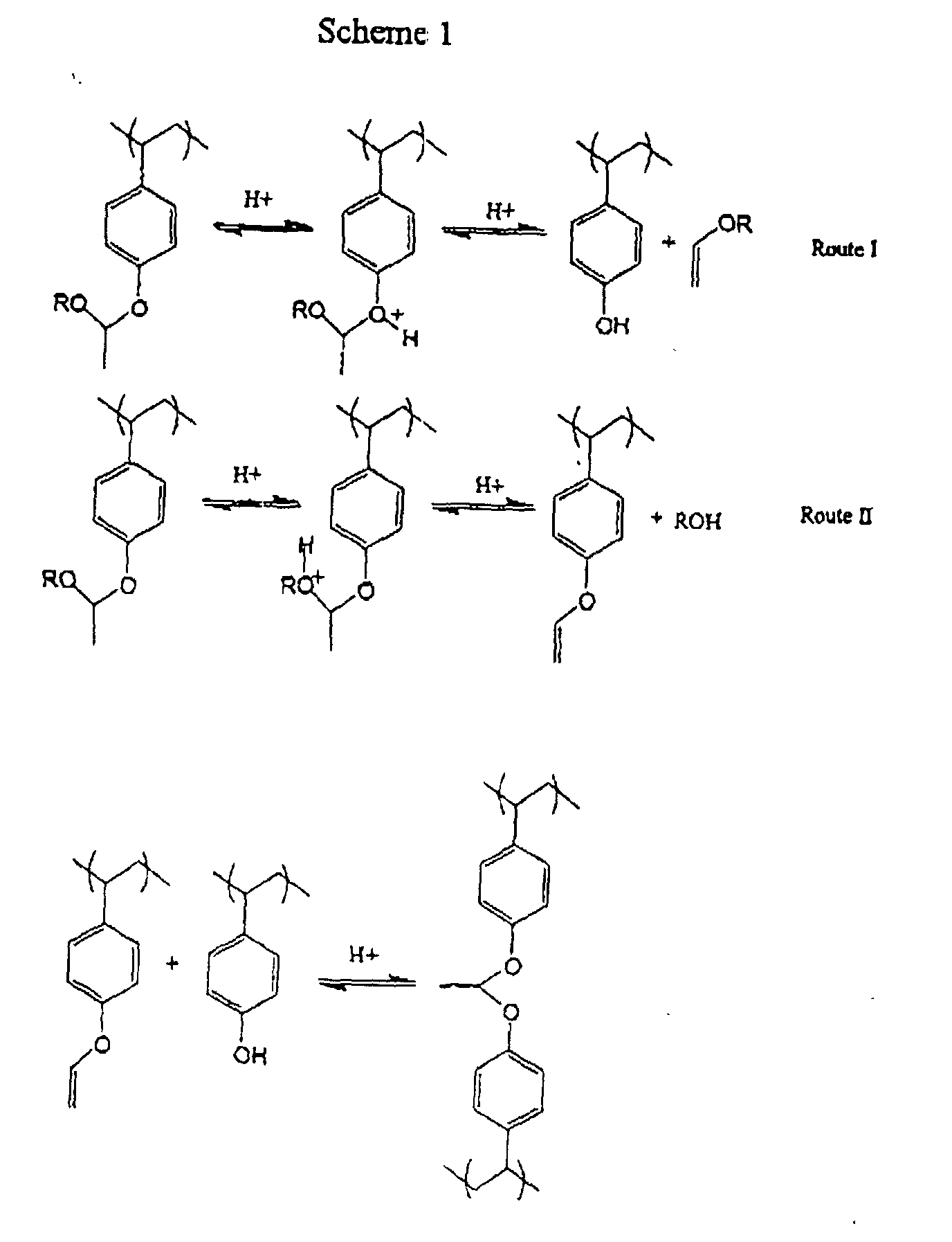
  • Without being bound by any theory, the following Scheme 1 depicts two possible routes (Routes 1 and 2) of reaction for an acetal resist units. Route II is a crosslinking reaction which will be favored where the depicted R has a substituted carbon linked to the oxygen (i.e. a secondary or tertiary oxygen) to thereby stabilize the oxonium ion intermediate that can undergo a transacetalization reaction (e.g. through a vinyl ether as exemplified by the phenoxy vinyl ether depicted below). Route I will be largely driven by an excess of acid, which will be present as photogenerated acid in exposed regions of the a resist layer. Route II also is promoted by acid, which can be present from adsorption from the external environment, diffusion of photogenerated acid into unexposed resist layers, or otherwise present such ass residual acid from the resist resin synthesis. A thermal acid generator that is activated at post-development hard bake temperatures also can be employed to promote the crosslinking reaction, although such a thermal acid generator is generally less preferred as discussed above.
    Figure 00080001
    It is also preferred to include cycloalkyl (e.g. cyclhexyl, cyclopentyl) units in a polymer with acetal substituents. Such acetal units, particularly formed with secondary or tertiary vinyl ethers (e.g. cyclohexylvinyl ether or t-butlyvinyl ether), can proceed at relatively low hard-bake temperatures, For instance, Scheme 2 below depicts such a suitable system, where the cycloalkyl units are depicted as pendant cyclohexyl groups substituted with acetal moietics. In Scheme 2, Route III depicts the deblocking reaction, and Route IV depicts a crosslinking reaction.
    Figure 00090001
    As discussed above, polymers of the invention also include units that undergo reaction in the presence of photogenerated acid, particularly a cleavage reaction to provide polar moieties such as carboxy (COOH), or hydroxy. Such acid labile groups are suitably pendant to the polymer backbone. Acrylate groups can be suitable and can be formed by free radical or other condensation of monomers of one or more substituted or unsubstituted alkyl acrylates such as t-butylacrylate and t-butylmethacrylate. Acrylacetate groups are also generally preferred and can be formed by free radical or other condensation of monomers of one or more substituted or unsubstituted alkyl acrylates such as t-butylacrylacetate, t-butylacryloxyacetate and t-butylmethacryloxyacetate. Suitable monomers are commercially available or can be readily prepared by known procedures. The pendant substituted ester moiety of the condensed acrylate unit, i.e. R-O-C(=O)-, serves as the pendant acid labile groups. A wide variety of acrylate units may be employed including those having an ester group (group R above) that is a non-cyclic or cyclic alkyl having 1 to about 14 carbon atoms, more typically 1 to about 8 carbons. Preferably the group R may be a tertiary non-cyclic alkyl such as t-butyl, or a second or tertiary alicyclic group such as adamantyl including 2-methyladamantyl, isobornyl, norbomyl and the like. Also suitable will be such alkyl ester groups that have one or more substituents such as halogen, particularly F, Cl or Br, C1-6 alkoxy, aryl such as phenyl, etc. Exemplary compounds that may be condensed to provide acrylate units of the polymers of the invention include butylacryloxyacetate including t-butylacryloxyacetate, butylmethacryloxyacetate including t-butylmethacryloxyacetate, etc. Suitable acrylate acid-labile groups also include those of the formula R3O(C=O)R2R1C- where R1 and R2 are each independently selected from the group of hydrogen, substituted or unsubstituted C1-10 alkyl. substituted or unsubstituted alkyloxyacetate or an electron-withdrawing group such as halogen; and R3 is substituted or unsubstituted C1-14 alkyl, substituted or unsubstituted aryl such as phenyl or substituted or unsubstituted aryalkyl such as benzyl. The substituents of substituted groups can be, e.g., halogen, C1-6 alkyl, C1-6 alkoxy, phenyl or other aryl, etc. Such acetate groups may be provided as described above for acrylate groups, i.e., by free radical or other condensation of monomers of one or more substituted or unsubstituted vinyl acetates such as allyl acetate and the like. Other suitable acid labile groups include those disclosed e.g. in U.S. Patent Nos, 5,362,600; 4,968,581; 4,883,740; 4,810,613; and 4,491,628.
    Generally preferred however, are polymers that contain mixed acetal units, e.g. acetai units that have primary alkyl substitution (e.g. R1 in Formula I above is a primary alkyl) that will readily undergo photoacid-induced cleavage, and secondary and tertiary acetals (e.g. R1 in Formula I above is a secondary or tertiary alkyl) that will undergo thermally-induced crosslinking in non-exposed resist areas after development.
    Polymers of the invention may comprise units in addition to crosslinking groups groups and acid labile groups. For instance, a polymer of the invention may contain phenolic units such as may be provided by reaction of hydroxystyrene or hydroxy(α-methyl)styrene, acid units such as may be provided by reaction of acrylic acid, methacrylic acid, and the like. Polymers of the invention also may suitably contain units that are essentially unreactive under typical lithographic conditions (photoacid and temperatures of about up to 180°C for no more than about 60 seconds) such as phenyl groups that may be provided by reaction of styrene, and alkyl and alicyclic groups such as may be provided by various vinyl monomers e.g. vinyl norborene and the like. Other preferred polymer units include nitrile units such as may be provided by reaction of acrylonitrile and methacrylonitrile.
    References herein to "optionally substituted" moieties or "substituted" moieties indicate that the specified group may be substituted with a relatively wide variety of non-hydrogen groups such as halogen (particularly F, Cl or Br), C1-8 alkyl, C1-8 alkoxy, aryl particularly carbocyclic aryl such as phenyl, nitro, cyano, C1-8 alkylsulfonyl such as mesyl and the like.
    Polymers of the invention can be prepared e.g. by free radical polymerization, e.g. by reaction of a plurality of monomers to provide the various units as discussed above in the presence of a radical initiator under an inert atmosphere (e.g., N2 or argon) and at elevated temperatures such as about 70° C or greater, although reaction temperatures may vary depending on the reactivity of the particular reagents employed and the boiling point of the reaction solvent (if a solvent is employed). See the examples which follow for exemplary reactions conditions. Suitable reaction temperatures for any particular system can be readily determined empirically by those skilled in the art based on the present disclosure.
    A reaction solvent may be employed if desired. Suitable solvents include propyleneglycol monomethylether acetate (PMA), or alcohols such as propanols and butanols as well as aromatic solvents such as benzene, chlorobenzene, toluene and xylene, Dimethyl sulfoxide and dimethylformamide are also suitable. The polymerization reaction also may be run neat.
    A variety of free radical initiators may be employed to prepare the copolymers of the invention. For example, azo compounds may be employed such as azo-bis-2,2'-isobutyronitrile (AIBN) and 1,1'-azo-bis(cyclohexanecarbonitrile). Peroxides, peresters, peracids and persulfates also can be employed.
    Monomers that contain hydroxy (such as para-hydroxystyrene) or other reactive moieties may be condensed in "masked" form if desired to facilitate polymer synthesis. For example para-acetoxystyrene may be employed as a "masked" form of para-hydroxystyrene. Other hydroxy masking or protecting groups also will be suitable such as alkylsilyl groups (to form silylethers with the hydroxy moiety), e.g. (CH3)3Si-, (CH3)2(butyl)Si-, ((CH3)3C)3Si-, etc.; other alkyl esters, e.g. CH3CH2C(=O)-, etc. After reaction completion, the masking groups may be removed under basic conditions. For example, the formed polymer may be heated in the presence of a base such as NH4OH or NH4OAc.
    A resin may have a generally minor amount of units that can undergo post-development hard-bake crosslinking. For example, suitably less than about 50 mole percent of total polymer units may be reactive to post-development, hard-bake crosslinking, such as up to about 10, 20, 30, 40 or 45 mole percent of total polymer units. If desired, higher amounts of the crosslinkable-groups also could be employed.
    Generally preferred polymers for use in resists of the invention may have a weight average molecular weight (Mw) of 1,000 to about 100,000, more preferably about 2,000 to about 30,000 with a molecular weight distribution (Mw/Mn) of about 3 or less, more preferably a molecular weight distribution of about 2 or less. Molecular weights (either Mw or Mn) of the polymers of the invention are suitably determined by gel permeation chromatography Suitable molecular weight distributions of copolymers of the invention include from about 1 to 5, more typically from about 1 to 3 or 4.
    As discussed above, resists of the invention also may comprise a thermal acid generator compound that will be significantly activated only at post-development hard-bake temperatures, i.e. the thermal acid generator is stable to typical soft-bake (90°C-110°C for 60 seconds) and post-exposure, pre-development (120°C for 60 seconds) thermal treatments. For example, a suitable thermal acid generator is nitrobenzylmesitylate which generates acid at about 160°C, a generally preferred hard-bake temperature. The thermally generated acid can promote crosslinking of resist components, as discussed above with respect to Route II of Scheme 1 and Route IV of Scheme 2.
    Resists of the invention also will comprise a photoactive component in addition to a resin component. Photoactivation of a coating layer of the resist results in a cleavage or other reaction of the polymer acid labile groups, The polymer component should be used in an amount sufficient to render a coating layer of the resist developable with an aqueous alkaline developer. The photoactive compounds typically includes a photoacid generator (i.e. "PAG") that is suitably employed in an amount sufficient to generate a latent image in a coating layer of the resist upon exposure to activating radiation.
    One group of preferred PAGs for use in the resists of the invention include imidosulfonates such as compounds of the following formula:
    Figure 00130001
    wherein R is camphor, adamantane, alkyl (e.g. C1-12 alkyl) and perfluoroalkyl such as perfluoro(C1-12alkyl), particularly perfluoro anions of perfluorooctanesulfonate, perfluorononanesulfonate and the like. A specifically preferred PAG is N-[(perfluorooctanesulfonyl)oxy]-5-norbornene-2,3-dicarboximide.
    Sulfonate compounds are also may be employed such as sulfonate salts. Two suitable agents are the following PAGs 1 and 2:
    Figure 00140001
    Such sulfonate compounds can be prepared as disclosed in European Patent Application 96118111.2 (publication number 0783136.
    Also suitable are the above two iodonium compounds complexed with anions other than the above-depicted groups. In particular, preferred anions include those of the formula RSO3 - where R is adamantane, alkyl (e.g. C1-12 alkyl) and perfluoroalkyl such as perfluoro (C1-12 alkyl), particularly perfluoro counter anions of perfluorooctanesulfonate, perfluorononanesulfonate and the like.
    Other known PAGs also may be employed in the resists of the invention. For example, N-sulfonyloxyimides may be employed such as those described in International application WO94/10608, or non-ionic halogenated PAGs that generate a halogen acid (e.g. HBr) upon exposure to activating radiation as described e.g. in. U.S. Patent 5,128,232 to Thackeray et al. and in European Patent Application Nos. 0164248 and 0232972.
    A preferred optional component of resist compositions of the invention is a dye compound. Preferred dyes can enhance resolution of the patterned resist image, typically by reducing reflections and the effects thereof (e.g. notching) of the exposure radiation. Preferred dyes include substituted and unsubstituted phenothiazine, phenoxazine, anthracene and anthrarobin compounds. Preferred substituents of substituted phenothiazine, phenoxazine, anthracene and anthrarobin include e.g. halogen, C1-12 alkyl, C1-12 alkoxy, C2-12 alkenyl, C1-12 alkanoyl such as acetyl, aryl such as phenyl, etc. Copolymers of such compounds also may be used as a dye, e.g. an anthracene acrylate polymer or copolymer.
    Another preferred optional additive is an added base, particularly tetrabutylammonium hydroxide (TBAH), or a lactate salt of TBAH, which can enhance resolution of a developed resist relief image. The added base used in relatively small amounts, e.g. about 1 to 20 percent by weight relative to the photoactive component (PAG).
    Photoresists of the invention also may contain other optional materials. For example, other optional additives include anti-striation agents, plasticizers, speed enhancers, etc. Such optional additives typically will be present in minor concentrations in a photoresist composition except for fillers and dyes which may be present in relatively large concentrations such as, e.g. in amounts of from about 5 to 30 percent by weight of the total weight of a resist's dry components.
    The compositions of the invention can be readily prepared by those skilled in the art. For example, a photoresist composition of the invention can be prepared by admixing the components of the photoresist in a suitable solvent such as, for example, ethyl lactate, a glycol ether such a 2-methoxyethyl ether (diglyme), ethylene glycol monomethyl ether, propylene glycol monomethyl ether, a Cellosolve ester such as methyl ethyl ketone; and 3-ethoxy ethyl propionate. Typically, the solids content of the composition varies between about 5 and 35 percent by weight of the total weight of the photoresist composition. The resin binder and PAG components should be present in amounts sufficient to provide a film coating layer and formation of good quality latent and relief images.
    The compositions of the invention are used in accordance with generally known procedures. The liquid coating compositions of the invention are applied to a substrate such as by spinning, dipping, roller coating or other conventional coating technique. When spin coating, the solids content of the coating solution can be adjusted to provide a desired film thickness based upon the specific spinning equipment utilized, the viscosity of the solution, the speed of the spinner and the amount of time allowed for spinning.
    The resist compositions of the invention are suitably applied to substrates conventionally used in processes involving coating with photoresists. For example, the composition may be applied over silicon or silicon dioxide wafers for the production of microprocessors and other integrated circuit components. Aluminum-aluminum oxide, gallium arsenide, ceramic, quartz or copper substrates also may be employed. Substrates used for liquid crystal display and other flat panel display applications are also suitably employed, e.g. glass substrates, indium tin oxide coated substrates and the like.
    Following coating of the photoresist onto a surface, it is dried by heating to remove the solvent until preferably the photoresist coating is tack free. Thereafter, it is imaged through a mask in conventional manner. The exposure is sufficient to effectively activate the photoactive component of the photoresist system to produce a patterned image in the resist coating layer and, more specifically, the exposure energy typically ranges from about 1 to 300 mJ/cm2, dependent upon the exposure tool and the components of the photoresist composition.
    Coating layers of the resist compositions of the invention arc preferably photoactivated by an exposure wavelength in the deep UV range i.e., 350 nm or less, more typically in the range of about 300 nm or less, typically about 150 to 300 or 450 nm, Particularly preferred exposures wavelength include 248 nm, 193 nm and 157 nm.
    Following exposure, the film layer of the composition is preferably baked at temperatures ranging from about 70° C to about 120° C. Thereafter, the film is developed. The exposed resist film is rendered positive working by employing a polar developer, preferably an aqueous based developer such as an inorganic alkali exemplified by sodium hydroxide, potassium hydroxide, sodium carbonate, or sodium bicarbonate.
    Following development of the photoresist coating over the substrate, the coated substrate is then thermally treated (hard-bake), e.g. to at least about 120°C, more preferably at least about 130°C, 140°C or 150°C for a time sufficient to both flow the resist and to induce crosslinking of resist component(s), Preferred hard-bake temperatures are from about 130°C to about 200°C, 210°C, 220°C, 230°C, 240°C, or 250°C, more typically 130°C, 140°C 150°C or 160°C to about 180°C, 190°C or 200°C. Post-development hard-bake temperatures of at least about 150°C, 160°C, 170°C, 180°C or 190°C also will be suitable. The post-development hard-bake may suitably be for about at least about 0.25, 0.5 1 or 2 minutes. Hard-bake in excess of about 2, 3 or 4 minutes are generally less preferred.
    Thereafter, the substrate may be processed as desired. For the manufacture of microelectronic substrates, e.g., the manufacture of silicon dioxide wafers, suitable etchants include a gas etchant, e.g. a chlorine or fluorine-based etchant such a CF4 or CF4/CHF3 etchant applied as a plasma stream. After such processing, resist may be removed from the processed substrate using known stripping procedures.
    All documents mentioned herein are fully incorporated herein by reference. The following non-limiting examples are illustrative of the invention.
    Example 1: GPC evaluations
    Acetal-blocked poly(hydroxystyrene) was prepared with a primary (ethyl vinyl ether) and a tertiary vinyl ether (t-butylvinyl ether). Several resist formulations were prepared (see below; identified as Resists 1, 2, 3 and 4) and then spin-coated onto silicon wafers, soft-baked at less than about 110°C, exposed (6% PSM contact hole mask) to 248 nm radiation, developed with aqueous alkaline solution, post-exposure baked at not in excess of about 120°C, and hardbaked at not less than 130°C. The resists were then washed off the wafer and analyzed by GPC to monitor molecular weight distribution. For all the resists there was an increase in the high molecular weight distribution of the polymer after the resist was hardbakcd (relative to the softbake or the resist alone). This would indicate that there is crosslinking (transacetalization) occurring during the hardbake.
    A. Resist and Resin Preparation
  • Resist 1: Resist 1 has the following components formulated with a solvent that comprised ethyl lactate:
  • 1. Polymer: poly(hydroxystyrene) that had phenolic sites blocked with t-butyl vinyl ether and t-butyloxycarbonyl-acid labile groups;
  • 2. Photoacid generator (PAG) of di-tert-butylphenyliodonium camphor sulfonate; and
  • 3. tetra-butyl ammonium hydroxide.
  • Resist 2: Resist 2 has the following components formulated with a solvent that comprised ethyl lactate:
  • 1. Polymer: poly(hydroxystyrene) that had phenolic sites blocked with t-butyl vinyl ether and tBOC-acid labile groups; and
  • 2. Photoacid generator (PAG) of di-tert-butylphenyliodonium camphor sulfonate.
  • Resist 3: Resist 3 has the following components formulated with a solvent that comprised ethyl lactate:
  • 1. Polymer: poly(hydroxystyrene) that had phenolic sites blocked with t-butyl vinyl ether and tBOC-acid labile groups;
  • 2. Photoacid generator (PAG) of di-tert-butylphenyliodonium camphor sulfonate;
  • 3. tetra-butyl ammonium hydroxide; and
  • 4. surfactant of FC-93.
  • Resist 4 (control). Resist 4 has the following components formulated with a solvent that comprised ethyl lactate:
  • 1. Polymer: poly(hydroxystyrene) that had phenolic sites blocked with ethyl vinyl ether and tBOC-acid labile groups;
  • 2. Photoacid generator (PAG) of di-tert-butylphenyliodonium camphor sulfonate; and
  • 3. tetra-butyl ammonium hydroxide.
  • A partially hydrogenated poly(hydroxystyrene) (i.e. contains cyclohexyl alcohol units) also was prepared where the phenolic or cyclohexyl alcohol units were reacted with t-butylvinyl ether. GPC analysis of the reaction mixture indicated a large increase in the high molecular weight distribution of this polymer. The cyclohexyl t-butyl acetal groups produced such favorable conditions for trasacetaliztion that crosslinking occurred during the blocking reaction.
    B. Resist evaluation for thermal flow margin.
    Resists 1,2,3, and 4 were evaluated for thermal flow. 180 nm contact holes were hardbaked at 145°C, 150°C, 155°C, and 160°C. For the resists containing the t-butylvinyl ether, there was a significant decrease in the flow rate relative to the ethylvinyl ether-blocked poly(hydroxystyrene) control. This result indicates that the use of a tertiary vinyl ether (and secondary vinyl ether ) blocking groups produces improved thermal flow margin.
    The foregoing description of the invention is merely illustrative thereof, and it is understood that variations and modification can be made without departing from the spirit or scope of the invention as set forth in the following claims.
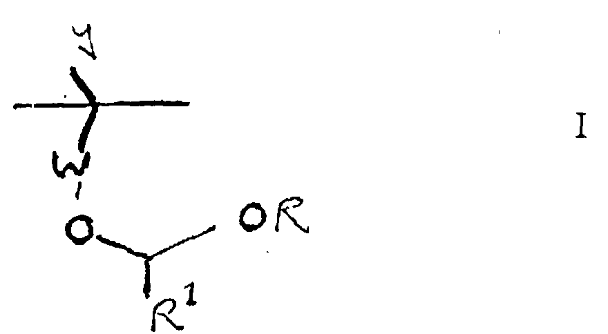
    Claims (30)

    1. A positive photoresist composition comprising a photoactive component and a polymer that comprises 1) groups reactive to crosslinking; and 2) photoacid-labile groups.
    2. The photoresist of claim 1 wherein groups 1) comprise acetal groups or ester groups.
    3. The photoresist of claim 1 wherein groups 1) comprise acetal groups.
    4. The photoresist of claim 3 wherein the acetal group have an oxygen linkage that is substituted by a secondary or tertiary carbon.
    5. The photoresist of claim 3 or 4 wherein the polymer comprises units of the following Formula I:
      Figure 00200001
      wherein W is a linker group;
      R is an optionally substituted cyclic or non-cyclic alkyl group;
      R1 is hydrogen or a cyclic or non-cyclic alkyl group;
      Y is hydrogen or optionally substituted alkyl.
    6. The photoresist of any one of claims 1 through 5 wherein the polymer comprises phenolic units.
    7. The photoresist of any one of claims 1 through 6 wherein the polymer comprises cycloalkyl units.
    8. The photoresist of claim 1 wherein the polymer comprises alkyl acrylate photoacid labile groups.
    9. A positive photoresist composition comprising a photoactive component and a component that comprises groups reactive to crosslinking, and a component that comprises photoacid-labile groups.
    10. The photoresist of claim 9 wherein the component with crosslinking groups and the component with photoacid-labile groups are a single component of the photoresist.
    11. The photoresist of claim 9 wherein the component with crosslinking groups and the component with photoacid-labile groups are separate components of the photoresist.
    12. The photoresist of claim 10 or 11 wherein the crosslinking groups are acetal groups.
    13. The photoresist of claim 12 wherein the acetal group have an oxygen linkage that is substituted by a secondary or tertiary carbon.
    14. The photoresist of any one of claims 1 through 13 wherein the polymer is substantially free of aromatic groups.
    15. The photoresist of any one of claims 1 through 14 wherein the photoresist comprises a thermal acid generator compound.
    16. The photoresist of any one of claims 1 through 14 wherein the photoresist is free of a thermal acid generator compound,
    17. A method for treating a microelectronic wafer substrate, comprising:
      a) applying a layer of a photoresist composition of any one of claims I through 16 on the microelectronic substrate; and
      b) exposing and developing the photoresist layer on the substrate to yield a developed photoresist layer;
      c) thermally treating the developed photoresist layer to induce crosslinking of one or more photoresist components.
    18. The method of claim 17 wherein the substrate is a microelectronic wafer.
    19. The method of claim 17 or 18 wherein the photoresist layer is exposed to patterned radiation having a wavelength of about 248 nm.
    20. The method of claim 17 or 18 wherein the photoresist layer is exposed to patterned radiation having a wavelength of less than 200 nm.
    21. The method of any one of claims 17 through 20 wherein the thermal treatment induces flow of the developed photoresist layer.
    22. The method of any one of claims 17 through 21 wherein the substrate comprises one or more contact holes.
    23. The method of claim 22 wherein the photoresist layer flows into the one or more contact holes during the thermal treatment.
    24. , The method of any one of claims 17 through 23 wherein the photoresist layer is heated after development to at least about 130°C.
    25. The method of any one of claims 17 through 23 wherein the photoresist layer is heated after development to at least about 150°C.
    26. The method of any one of claims 17 through 23 wherein the photoresist layer is heated after development to at least about 160°C.
    27. The method of any one of claims 17 through 26 wherein the photoresist is heated after exposure and prior to development at a temperature of not greater than about 120°C, and the pre-development heating does not cause substantial crosslinking of the photoresist layer.
    28. An article of manufacture comprising a substrate having coated thereon a photoresist composition of any one of claims 1 through 16.
    29. An article of claim 28 wherein the substrate is a microelectronic wafer.
    30. An article of claim 28 wherein the microelectronic wafer comprises one or more contact holes.
    EP01303145A 2000-04-03 2001-04-02 Photoresist compositions and use of same Withdrawn EP1143300A1 (en)

    Applications Claiming Priority (2)

    Application Number Priority Date Filing Date Title
    US19428700P 2000-04-03 2000-04-03
    US194287 2000-04-03

    Publications (1)

    Publication Number Publication Date
    EP1143300A1 true EP1143300A1 (en) 2001-10-10

    Family

    ID=22717002

    Family Applications (1)

    Application Number Title Priority Date Filing Date
    EP01303145A Withdrawn EP1143300A1 (en) 2000-04-03 2001-04-02 Photoresist compositions and use of same

    Country Status (5)

    Country Link
    US (1) US6828083B2 (en)
    EP (1) EP1143300A1 (en)
    JP (1) JP4695282B2 (en)
    KR (1) KR100891941B1 (en)
    TW (1) TWI226515B (en)

    Cited By (1)

    * Cited by examiner, † Cited by third party
    Publication number Priority date Publication date Assignee Title
    DE10147011B4 (en) * 2001-04-10 2006-10-19 Fujitsu Ltd., Kawasaki A chemically amplified resist composition and method of forming a patterned film using the same

    Families Citing this family (16)

    * Cited by examiner, † Cited by third party
    Publication number Priority date Publication date Assignee Title
    JP4790153B2 (en) * 2000-09-01 2011-10-12 富士通株式会社 Negative resist composition, method of forming resist pattern, and method of manufacturing electronic device
    TW594416B (en) * 2001-05-08 2004-06-21 Shipley Co Llc Photoimageable composition
    JP2003233190A (en) * 2001-10-09 2003-08-22 Shipley Co Llc Polymer with mixed photoacid-labile group and photoresist comprising the same
    US20030232273A1 (en) * 2001-10-09 2003-12-18 Shipley Company, L.L.C. Acetal/alicyclic polymers and photoresist compositions
    US7022455B2 (en) * 2001-12-28 2006-04-04 Shipley Company, L.L.C. Photoacid-labile polymers and photoresists comprising same
    CN100537053C (en) 2003-09-29 2009-09-09 Hoya株式会社 Mask blanks and method of producing the same
    JP2005173369A (en) * 2003-12-12 2005-06-30 Tokyo Ohka Kogyo Co Ltd Method for removing resist pattern
    WO2006052380A1 (en) * 2004-11-08 2006-05-18 Dupont Electronic Polymers L.P. Derivatized polyhydroxystryrene (dphs)with a novolak type structure and blocked dphs (bdphs) and processes for preparing the same
    US7741015B2 (en) * 2007-02-16 2010-06-22 Shin-Etsu Chemical Co., Ltd. Patterning process and resist composition
    US8512934B2 (en) 2007-10-10 2013-08-20 Basf Se Sulphonium salt initiators
    JP4826841B2 (en) * 2009-01-15 2011-11-30 信越化学工業株式会社 Pattern formation method
    JP4826840B2 (en) * 2009-01-15 2011-11-30 信越化学工業株式会社 Pattern formation method
    JP4826846B2 (en) * 2009-02-12 2011-11-30 信越化学工業株式会社 Pattern formation method
    WO2011104127A1 (en) 2010-02-24 2011-09-01 Basf Se Latent acids and their use
    JP6405772B2 (en) * 2014-07-31 2018-10-17 住友化学株式会社 Composition and organic thin film transistor using the same
    WO2016124493A1 (en) 2015-02-02 2016-08-11 Basf Se Latent acids and their use

    Citations (4)

    * Cited by examiner, † Cited by third party
    Publication number Priority date Publication date Assignee Title
    DE3920481A1 (en) * 1988-06-27 1990-01-25 Tech Hochschule C Schorlemmer Method for encapsulating semiconductor sensors
    EP0788031A1 (en) * 1996-02-05 1997-08-06 Fuji Photo Film Co., Ltd. Positive working photosensitive composition
    EP0939340A1 (en) * 1998-02-25 1999-09-01 International Business Machines Corporation Radiation sensitive resists
    EP0939339A1 (en) * 1998-02-25 1999-09-01 International Business Machines Corporation Irradiation sensitive positive-tone resists using polymers containing two acid sensitive protecting groups

    Family Cites Families (13)

    * Cited by examiner, † Cited by third party
    Publication number Priority date Publication date Assignee Title
    EP0543569B1 (en) * 1991-11-22 1999-03-10 AT&T Corp. Fabrication of phase-shifting lithographic masks
    JP3256064B2 (en) * 1993-08-18 2002-02-12 富士通株式会社 Method of forming resist pattern
    KR100293130B1 (en) * 1995-04-12 2001-09-17 카나가와 치히로 Polymer compound and chemically amplified positive resist material
    JP3700164B2 (en) * 1996-03-01 2005-09-28 Jsr株式会社 Radiation sensitive composition
    US5886102A (en) * 1996-06-11 1999-03-23 Shipley Company, L.L.C. Antireflective coating compositions
    JPH10147864A (en) * 1996-11-20 1998-06-02 Nec Corp Formation of thin film and sputtering device
    JPH10268508A (en) * 1997-01-27 1998-10-09 Shin Etsu Chem Co Ltd Partially hydrogenated polymer compound and chemically sensitized positive resist material
    US6358672B2 (en) * 1998-02-05 2002-03-19 Samsung Electronics Co., Ltd. Method of forming semiconductor device pattern including cross-linking and flow baking a positive photoresist
    TW594406B (en) * 1998-02-25 2004-06-21 Ibm Irradiation sensitive positive-tone resists using polymers containing two acid sensitive protecting groups
    KR100421034B1 (en) * 1999-04-21 2004-03-04 삼성전자주식회사 Resist composition and fine pattern forming method using the same
    KR100557585B1 (en) * 1999-10-29 2006-03-03 주식회사 하이닉스반도체 Photoresist composition for resist flow process and process for forming a contact hole using the same
    JP3755571B2 (en) * 1999-11-12 2006-03-15 信越化学工業株式会社 Chemically amplified positive resist material and pattern forming method
    JP4475372B2 (en) * 2000-03-22 2010-06-09 信越化学工業株式会社 Chemically amplified positive resist material and pattern forming method

    Patent Citations (4)

    * Cited by examiner, † Cited by third party
    Publication number Priority date Publication date Assignee Title
    DE3920481A1 (en) * 1988-06-27 1990-01-25 Tech Hochschule C Schorlemmer Method for encapsulating semiconductor sensors
    EP0788031A1 (en) * 1996-02-05 1997-08-06 Fuji Photo Film Co., Ltd. Positive working photosensitive composition
    EP0939340A1 (en) * 1998-02-25 1999-09-01 International Business Machines Corporation Radiation sensitive resists
    EP0939339A1 (en) * 1998-02-25 1999-09-01 International Business Machines Corporation Irradiation sensitive positive-tone resists using polymers containing two acid sensitive protecting groups

    Cited By (3)

    * Cited by examiner, † Cited by third party
    Publication number Priority date Publication date Assignee Title
    DE10147011B4 (en) * 2001-04-10 2006-10-19 Fujitsu Ltd., Kawasaki A chemically amplified resist composition and method of forming a patterned film using the same
    US7129017B2 (en) 2001-04-10 2006-10-31 Fujitsu Limited Chemically amplified resist composition and method for forming patterned film using same
    KR100750225B1 (en) * 2001-04-10 2007-08-31 후지쯔 가부시끼가이샤 Chemically amplified resist composition and method for forming patterned film using same

    Also Published As

    Publication number Publication date
    JP4695282B2 (en) 2011-06-08
    KR20010095279A (en) 2001-11-03
    US6828083B2 (en) 2004-12-07
    TWI226515B (en) 2005-01-11
    KR100891941B1 (en) 2009-04-08
    US20010053496A1 (en) 2001-12-20
    JP2001356481A (en) 2001-12-26

    Similar Documents

    Publication Publication Date Title
    US6057083A (en) Polymers and photoresist compositions
    US6165674A (en) Polymers and photoresist compositions for short wavelength imaging
    JP5810139B2 (en) Photoresist composition comprising a blend of photoacid generators
    US6828083B2 (en) Photoresist compositions and use of same
    US5962184A (en) Photoresist composition comprising a copolymer of a hydroxystyrene and a (meth)acrylate substituted with an alicyclic ester substituent
    US6989224B2 (en) Polymers with mixed photoacid-labile groups and photoresists comprising same
    JP2004163877A (en) Novel resin and photoresist composition containing the same
    US20030232273A1 (en) Acetal/alicyclic polymers and photoresist compositions
    US20020012869A1 (en) Positive photoresists containing crosslinked polymers
    US7326518B2 (en) Photoresist compositions
    US6077643A (en) Polymers and photoresist compositions
    US6773872B2 (en) Reduction of inorganic contaminants in polymers and photoresist compositions comprising same
    US6852466B2 (en) Photoresist compositions particularly suitable for short wavelength imaging
    US7022455B2 (en) Photoacid-labile polymers and photoresists comprising same
    US6492087B1 (en) Polymers and photoresist compositions comprising same
    US6770413B1 (en) Hydroxyphenyl copolymers and photoresists comprising same
    JPH10268519A (en) Novel polymer and photoresist composition containing same
    JPH11338151A (en) Positive type photosensitive composition
    US20050186507A1 (en) Photoresist composition
    US20020051938A1 (en) Novel polymers and photoresist compositions for short wavelength imaging

    Legal Events

    Date Code Title Description
    PUAI Public reference made under article 153(3) epc to a published international application that has entered the european phase

    Free format text: ORIGINAL CODE: 0009012

    17P Request for examination filed

    Effective date: 20010410

    AK Designated contracting states

    Kind code of ref document: A1

    Designated state(s): DE FR GB IT NL

    Kind code of ref document: A1

    Designated state(s): AT BE CH CY DE DK ES FI FR GB GR IE IT LI LU MC NL PT SE TR

    AX Request for extension of the european patent

    Free format text: AL;LT;LV;MK;RO;SI

    AKX Designation fees paid

    Free format text: DE FR GB IT NL

    17Q First examination report despatched

    Effective date: 20090519

    STAA Information on the status of an ep patent application or granted ep patent

    Free format text: STATUS: THE APPLICATION IS DEEMED TO BE WITHDRAWN

    18D Application deemed to be withdrawn

    Effective date: 20090930