EP1139436A2 - Solar cell device - Google Patents
Solar cell device Download PDFInfo
- Publication number
- EP1139436A2 EP1139436A2 EP01107699A EP01107699A EP1139436A2 EP 1139436 A2 EP1139436 A2 EP 1139436A2 EP 01107699 A EP01107699 A EP 01107699A EP 01107699 A EP01107699 A EP 01107699A EP 1139436 A2 EP1139436 A2 EP 1139436A2
- Authority
- EP
- European Patent Office
- Prior art keywords
- solar cell
- substrate
- layer
- thin film
- conductive material
- Prior art date
- Legal status (The legal status is an assumption and is not a legal conclusion. Google has not performed a legal analysis and makes no representation as to the accuracy of the status listed.)
- Withdrawn
Links
- 229910052751 metal Inorganic materials 0.000 claims abstract description 68
- 239000002184 metal Substances 0.000 claims abstract description 68
- 239000010409 thin film Substances 0.000 claims abstract description 54
- 239000011888 foil Substances 0.000 claims abstract description 47
- 239000004065 semiconductor Substances 0.000 claims abstract description 17
- 238000005323 electroforming Methods 0.000 claims abstract description 14
- 239000004020 conductor Substances 0.000 claims description 53
- 238000001579 optical reflectometry Methods 0.000 claims description 6
- 239000000758 substrate Substances 0.000 abstract description 82
- XLOMVQKBTHCTTD-UHFFFAOYSA-N Zinc monoxide Chemical compound [Zn]=O XLOMVQKBTHCTTD-UHFFFAOYSA-N 0.000 description 31
- 238000006243 chemical reaction Methods 0.000 description 31
- XOLBLPGZBRYERU-UHFFFAOYSA-N tin dioxide Chemical compound O=[Sn]=O XOLBLPGZBRYERU-UHFFFAOYSA-N 0.000 description 31
- 229910001887 tin oxide Inorganic materials 0.000 description 19
- RYGMFSIKBFXOCR-UHFFFAOYSA-N Copper Chemical compound [Cu] RYGMFSIKBFXOCR-UHFFFAOYSA-N 0.000 description 16
- 239000011521 glass Substances 0.000 description 16
- 229910021417 amorphous silicon Inorganic materials 0.000 description 14
- AMGQUBHHOARCQH-UHFFFAOYSA-N indium;oxotin Chemical compound [In].[Sn]=O AMGQUBHHOARCQH-UHFFFAOYSA-N 0.000 description 14
- 239000011889 copper foil Substances 0.000 description 13
- 239000011787 zinc oxide Substances 0.000 description 13
- 229910052709 silver Inorganic materials 0.000 description 10
- BQCADISMDOOEFD-UHFFFAOYSA-N Silver Chemical compound [Ag] BQCADISMDOOEFD-UHFFFAOYSA-N 0.000 description 9
- 239000004332 silver Substances 0.000 description 9
- 238000004544 sputter deposition Methods 0.000 description 9
- 229910052782 aluminium Inorganic materials 0.000 description 7
- 239000003792 electrolyte Substances 0.000 description 7
- 239000000463 material Substances 0.000 description 7
- XKRFYHLGVUSROY-UHFFFAOYSA-N Argon Chemical compound [Ar] XKRFYHLGVUSROY-UHFFFAOYSA-N 0.000 description 6
- PXHVJJICTQNCMI-UHFFFAOYSA-N Nickel Chemical compound [Ni] PXHVJJICTQNCMI-UHFFFAOYSA-N 0.000 description 6
- XAGFODPZIPBFFR-UHFFFAOYSA-N aluminium Chemical compound [Al] XAGFODPZIPBFFR-UHFFFAOYSA-N 0.000 description 6
- 238000000034 method Methods 0.000 description 6
- XEEYBQQBJWHFJM-UHFFFAOYSA-N Iron Chemical compound [Fe] XEEYBQQBJWHFJM-UHFFFAOYSA-N 0.000 description 5
- VEXZGXHMUGYJMC-UHFFFAOYSA-N Hydrochloric acid Chemical compound Cl VEXZGXHMUGYJMC-UHFFFAOYSA-N 0.000 description 4
- 238000007598 dipping method Methods 0.000 description 4
- 238000004519 manufacturing process Methods 0.000 description 4
- QTBSBXVTEAMEQO-UHFFFAOYSA-N Acetic acid Chemical compound CC(O)=O QTBSBXVTEAMEQO-UHFFFAOYSA-N 0.000 description 3
- BLRPTPMANUNPDV-UHFFFAOYSA-N Silane Chemical compound [SiH4] BLRPTPMANUNPDV-UHFFFAOYSA-N 0.000 description 3
- 229910052786 argon Inorganic materials 0.000 description 3
- 239000011248 coating agent Substances 0.000 description 3
- 238000000576 coating method Methods 0.000 description 3
- 229910052802 copper Inorganic materials 0.000 description 3
- 239000010949 copper Substances 0.000 description 3
- 229960000355 copper sulfate Drugs 0.000 description 3
- 229910000365 copper sulfate Inorganic materials 0.000 description 3
- ARUVKPQLZAKDPS-UHFFFAOYSA-L copper(II) sulfate Chemical compound [Cu+2].[O-][S+2]([O-])([O-])[O-] ARUVKPQLZAKDPS-UHFFFAOYSA-L 0.000 description 3
- 239000010408 film Substances 0.000 description 3
- 239000007789 gas Substances 0.000 description 3
- 229910052759 nickel Inorganic materials 0.000 description 3
- 238000002310 reflectometry Methods 0.000 description 3
- 229920005989 resin Polymers 0.000 description 3
- 239000011347 resin Substances 0.000 description 3
- 238000005096 rolling process Methods 0.000 description 3
- HBMJWWWQQXIZIP-UHFFFAOYSA-N silicon carbide Chemical compound [Si+]#[C-] HBMJWWWQQXIZIP-UHFFFAOYSA-N 0.000 description 3
- 239000010935 stainless steel Substances 0.000 description 3
- 229910001220 stainless steel Inorganic materials 0.000 description 3
- 239000004642 Polyimide Substances 0.000 description 2
- 239000002253 acid Substances 0.000 description 2
- 239000002390 adhesive tape Substances 0.000 description 2
- 239000007864 aqueous solution Substances 0.000 description 2
- DQXBYHZEEUGOBF-UHFFFAOYSA-N but-3-enoic acid;ethene Chemical compound C=C.OC(=O)CC=C DQXBYHZEEUGOBF-UHFFFAOYSA-N 0.000 description 2
- 238000010586 diagram Methods 0.000 description 2
- 238000005516 engineering process Methods 0.000 description 2
- 238000005530 etching Methods 0.000 description 2
- 239000005038 ethylene vinyl acetate Substances 0.000 description 2
- 229910052742 iron Inorganic materials 0.000 description 2
- 238000010030 laminating Methods 0.000 description 2
- 239000007769 metal material Substances 0.000 description 2
- 229920001200 poly(ethylene-vinyl acetate) Polymers 0.000 description 2
- 229920001721 polyimide Polymers 0.000 description 2
- 238000010248 power generation Methods 0.000 description 2
- 238000002230 thermal chemical vapour deposition Methods 0.000 description 2
- 238000001039 wet etching Methods 0.000 description 2
- JPVYNHNXODAKFH-UHFFFAOYSA-N Cu2+ Chemical compound [Cu+2] JPVYNHNXODAKFH-UHFFFAOYSA-N 0.000 description 1
- CWYNVVGOOAEACU-UHFFFAOYSA-N Fe2+ Chemical compound [Fe+2] CWYNVVGOOAEACU-UHFFFAOYSA-N 0.000 description 1
- -1 ITO Chemical compound 0.000 description 1
- XUIMIQQOPSSXEZ-UHFFFAOYSA-N Silicon Chemical compound [Si] XUIMIQQOPSSXEZ-UHFFFAOYSA-N 0.000 description 1
- RTAQQCXQSZGOHL-UHFFFAOYSA-N Titanium Chemical compound [Ti] RTAQQCXQSZGOHL-UHFFFAOYSA-N 0.000 description 1
- 239000000853 adhesive Substances 0.000 description 1
- 230000001070 adhesive effect Effects 0.000 description 1
- 229910045601 alloy Inorganic materials 0.000 description 1
- 239000000956 alloy Substances 0.000 description 1
- 229910052787 antimony Inorganic materials 0.000 description 1
- WATWJIUSRGPENY-UHFFFAOYSA-N antimony atom Chemical compound [Sb] WATWJIUSRGPENY-UHFFFAOYSA-N 0.000 description 1
- 239000003245 coal Substances 0.000 description 1
- 150000001875 compounds Chemical class 0.000 description 1
- 229910001431 copper ion Inorganic materials 0.000 description 1
- 239000013078 crystal Substances 0.000 description 1
- 238000007872 degassing Methods 0.000 description 1
- 238000000151 deposition Methods 0.000 description 1
- 230000008021 deposition Effects 0.000 description 1
- 238000001312 dry etching Methods 0.000 description 1
- 229960002089 ferrous chloride Drugs 0.000 description 1
- 239000005357 flat glass Substances 0.000 description 1
- 239000002803 fossil fuel Substances 0.000 description 1
- IXCSERBJSXMMFS-UHFFFAOYSA-N hcl hcl Chemical compound Cl.Cl IXCSERBJSXMMFS-UHFFFAOYSA-N 0.000 description 1
- 230000010354 integration Effects 0.000 description 1
- NMCUIPGRVMDVDB-UHFFFAOYSA-L iron dichloride Chemical compound Cl[Fe]Cl NMCUIPGRVMDVDB-UHFFFAOYSA-L 0.000 description 1
- 229910021424 microcrystalline silicon Inorganic materials 0.000 description 1
- 238000012986 modification Methods 0.000 description 1
- 230000004048 modification Effects 0.000 description 1
- LNOPIUAQISRISI-UHFFFAOYSA-N n'-hydroxy-2-propan-2-ylsulfonylethanimidamide Chemical compound CC(C)S(=O)(=O)CC(N)=NO LNOPIUAQISRISI-UHFFFAOYSA-N 0.000 description 1
- DITXJPASYXFQAS-UHFFFAOYSA-N nickel;sulfamic acid Chemical compound [Ni].NS(O)(=O)=O DITXJPASYXFQAS-UHFFFAOYSA-N 0.000 description 1
- 239000003208 petroleum Substances 0.000 description 1
- 229910021420 polycrystalline silicon Inorganic materials 0.000 description 1
- 238000012545 processing Methods 0.000 description 1
- 239000012495 reaction gas Substances 0.000 description 1
- 238000012827 research and development Methods 0.000 description 1
- 238000005070 sampling Methods 0.000 description 1
- 238000007789 sealing Methods 0.000 description 1
- 229910052710 silicon Inorganic materials 0.000 description 1
- 239000010703 silicon Substances 0.000 description 1
- 238000000992 sputter etching Methods 0.000 description 1
- 238000001771 vacuum deposition Methods 0.000 description 1
Images

Classifications
-
- H—ELECTRICITY
- H10—SEMICONDUCTOR DEVICES; ELECTRIC SOLID-STATE DEVICES NOT OTHERWISE PROVIDED FOR
- H10F—INORGANIC SEMICONDUCTOR DEVICES SENSITIVE TO INFRARED RADIATION, LIGHT, ELECTROMAGNETIC RADIATION OF SHORTER WAVELENGTH OR CORPUSCULAR RADIATION
- H10F77/00—Constructional details of devices covered by this subclass
- H10F77/10—Semiconductor bodies
- H10F77/16—Material structures, e.g. crystalline structures, film structures or crystal plane orientations
- H10F77/169—Thin semiconductor films on metallic or insulating substrates
-
- H—ELECTRICITY
- H10—SEMICONDUCTOR DEVICES; ELECTRIC SOLID-STATE DEVICES NOT OTHERWISE PROVIDED FOR
- H10F—INORGANIC SEMICONDUCTOR DEVICES SENSITIVE TO INFRARED RADIATION, LIGHT, ELECTROMAGNETIC RADIATION OF SHORTER WAVELENGTH OR CORPUSCULAR RADIATION
- H10F77/00—Constructional details of devices covered by this subclass
- H10F77/40—Optical elements or arrangements
- H10F77/42—Optical elements or arrangements directly associated or integrated with photovoltaic cells, e.g. light-reflecting means or light-concentrating means
- H10F77/48—Back surface reflectors [BSR]
-
- Y—GENERAL TAGGING OF NEW TECHNOLOGICAL DEVELOPMENTS; GENERAL TAGGING OF CROSS-SECTIONAL TECHNOLOGIES SPANNING OVER SEVERAL SECTIONS OF THE IPC; TECHNICAL SUBJECTS COVERED BY FORMER USPC CROSS-REFERENCE ART COLLECTIONS [XRACs] AND DIGESTS
- Y02—TECHNOLOGIES OR APPLICATIONS FOR MITIGATION OR ADAPTATION AGAINST CLIMATE CHANGE
- Y02E—REDUCTION OF GREENHOUSE GAS [GHG] EMISSIONS, RELATED TO ENERGY GENERATION, TRANSMISSION OR DISTRIBUTION
- Y02E10/00—Energy generation through renewable energy sources
- Y02E10/50—Photovoltaic [PV] energy
- Y02E10/52—PV systems with concentrators
Definitions
- the present invention relates to a solar cell device, particularly relates to a technology for manufacturing a solar cell device having high photovoltaic conversion efficiency at low cost.
- a solar cell device is expected to replace fossil fuel such as petroleum and coal and to be a new energy source because it can provide clean energy without depletion.
- a solar cell device for generating power for household etc. has been developed and commercialized.
- a solar cell device, which uses a thin film semiconductor of such as an amorphous semiconductor, is easy to increase its area, and consequently research and development of such a solar cell device have been promoted.
- a substrate 21 having a rough surface for scattering light can be a substrate formed by laminating a metal layer of such as Ag and Al on a flat glass substrate with tin oxide (SnO 2 ), indium tin oxide (ITO), or zinc oxide (ZnO) interposed therebetween, a metal substrate having a rough surface, or a metal substrate coated with a metal layer having a rough surface.
- a photovoltaic conversion layer 22 composed of a thin semiconductor film containing mainly amorphous silicon, microcrystalline silicon or the like is formed on the substrate 21, and a transparent electrode layer 23 formed of transparent conductive material such as ITO is formed thereon.
- incident light such as sunlight is incident from a side of the transparent electrode film 23 formed of transparent conductive material such as ITO.
- a thin film solar cell device provided with a fine rough surface on a surface of a transparent substrate capable of improving photovoltaic conversion efficiency by the aid of light confinement is also well known.
- the substrate 21 of the solar cell device is heavy.
- the heavy weight of the solar cell module degrades workability.
- a solar cell device includes a photovoltaic layer of a thin film semiconductor layer having semiconductor junction in an inside formed on a metal foil formed by electroforming.
- the metal foil formed by electroforming has a rough shape of approximately 0.1-10 ⁇ m, more preferably 0.1-5 ⁇ m, of mean roughness depth (Rz) on a surface of the metal foil.
- This invention can provide a solar cell device for power generation capable of reducing cost for manufacture because through put in forming a rough shape, and cost for the rough-shaped metal foil substrate which is electroformed is less as compared with a substrate of a glass coated with the transparent conductive material of such as tin oxide, indium tin oxide, and zinc oxide. Furthermore, the thin film solar cell device using the rough-shaped substrate formed of a metal foil is light-weighted. Therefore, even when the size of the solar cell module increases, the weight is relatively small and workability is good.
- a transparent conductive material layer can be interposed between the metal foil and the thin film semiconductor layer.
- a conductive material layer and the transparent conductive material layer of high optical reflectivity can be interposed between the metal foil and the thin film semiconductor layer.
- a rough shape of approximately 0.02-0.5 ⁇ m of mean roughness depth (Rz) can be formed on a surface of the transparent conductive material layer.
- the transparent conductive material layer of such as tin oxide, indium tin oxide, and zinc oxide having a fine rough shape can be formed on the metal foil substrate. With this shape of the transparent conductive material layer, incident light such as sunlight can be effectively utilized and efficiency of the solar cell improves.
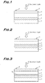
- Fig. 1 is a cross sectional view illustrating a structure of a thin film solar cell device of the first embodiment of the invention.
- a substrate 1 is a metal foil of copper, nickel, iron or the like of 10-500 ⁇ m in thickness produced by electroforming or a metal foil of alloy of these material.
- the substrate 1 used in this embodiment is an electroformed copper foil.
- “Wet processing handbook” (FOUNDATION ADVANCED TECHNOLOGY INSTITUTE, published on March 22, 1996, 108-123 pages) describes on electroforming, for example.
- a drum is dipped in an electrolyte bath, metal is deposited on the drum to be thick, and then the electrically deposited material is peeled from the drum to produce into product or duplicate.
- copper electrolyte used in electroforming is acid copper-sulfate containing copper-sulfate of 200g/l.
- a drum of titan, stainless steel or the like is partially dipped in the electrolyte bath filled with the acid copper-sulfate, and electrical deposition is made on a surface of the drum.
- the deposited material is sequentially peeled off and a band-shaped copper foil is produced.
- a positive electrode is insoluble anode (lead, antimony). The copper is chemically melted and supplemented when copper ions in the electrolyte bath reduce.
- the electroformed foil formed by such the method is different from a foil formed by rolling in that crystals are produced vertically to a face and an ideal rough shape for a substrate of a thin film solar cell can be obtained.
- the metal foil produced by the electroforming has a rough shape of approximately 0.1-10 ⁇ m of mean roughness depth (Rz).
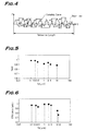
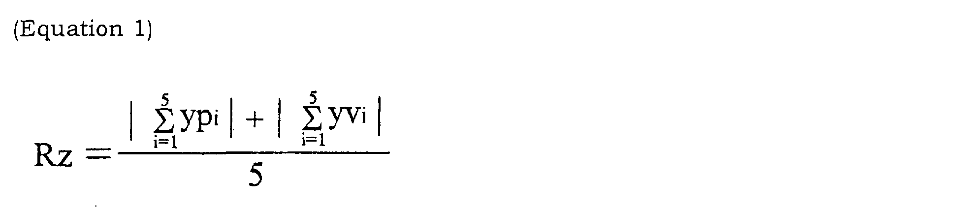
- Mean roughness depth (Rz) is explained in JIS B0601-1994. As shown in Fig. 4, average of absolute values of the five highest peaks from a mean line and average of absolute values of the five deepest valleys from the mean line within a reference length L of a sampling roughness curve are added to average and minimize diversity of heights. This is a parameter expressed by the following equation 1.
- nickel and iron foil can also be produced. For example, nickel is formed by dipping a drum in an electrolyte bath of nickel sulfamic acid. Iron is formed by dipping a drum in an electrolyte bath of ferrous chloride and ferrous sulfamic acid.
- a thickness of the metal foil substrate 1 formed by the electroforming is desired to be not less than 10 ⁇ m in viewpoint of its structure and mechanical strength in dealing.
- the metal foil substrate 1 is a copper foil of 18 ⁇ m in thickness and a height of the rough shape is 3 ⁇ m of mean roughness depth.
- transparent conductive material layer 2 of such as tin oxide, indium tin oxide, and zinc oxide is coated on the metal foil substrate 1 by thermal CVD or sputtering.
- zinc oxide (ZnO) of 500 ⁇ is coated on the substrate 1 by radio frequency (RF) sputtering.
- the layer is formed under the condition of argon (Ar) gas atmosphere, reaction pressure 0.665Pa, radio frequency power density 2W/cm 2 , substrate temperature of room temperature.
- a photovoltaic conversion layer 3 of a thin film semiconductor layer mainly containing amorphous silicon or the like is formed on the transparent conductive material layer 2.
- the photovoltaic conversion layer 3 of this embodiment is formed by laminating an n-type layer of amorphous silicon layer of 200 ⁇ , an i-type layer of amorphous silicon layer of 3000 ⁇ , and a p-type layer of amorphous silicon carbide layer of 100 ⁇ in this order from a side of the rough metal foil substrate 1. Conditions for forming each of the layers are shown in Table 1.
- a transparent electrode layer 4 of transparent conductive material such as indium tin oxide, and zinc oxide is formed on the photovoltaic conversion layer 3 by sputtering.
- indium tin oxide (ITO) of 700 ⁇ is formed by radio frequency (RF) sputtering.
- the layer is formed under conditions of argon (Ar) gas atmosphere, reaction pressure of 0.665Pa, radio frequency power density of 2W/cm 2 , and 200°C substrate temperature.
- a comb-shaped electrode 5 of such as aluminum and silver having good conductivity is formed on the transparent electrode layer 4.
- silver (Ag) is deposited by a vacuum evaporation method.
- a solar cell device 10 according to this invention is formed. Incident light 6 enters from a side of the transparent electrode layer 4.
- Fig. 2 is a cross sectional view illustrating a structure of a thin film solar cell device of the second embodiment.
- the same elements as in the first embodiment are given the same reference numbers and explanation of them are omitted to prevent duplication.
- a solar cell device 10 of the second embodiment is different from that of the first embodiment in that a metal layer 7 of relatively high reflectivity such as aluminum and silver is deposited so as to improve optical reflectivity of the substrate.
- the metal layer of high optical reflectivity of the second embodiment is formed by coating silver (Ag) of 3000 ⁇ in thickness on the rough metal foil substrate 1 by radio frequency (RF) sputtering.
- the silver is formed under the conditions of argon (Ar) gas atmosphere, reaction pressure of 0.399Pa, radio frequency power density of 3W/cm 2 , a substrate temperature of room temperature.
- a transparent conductive material layer 2 of such as tin oxide, indium tin oxide, and zinc oxide is coated on the metal layer 7 by sputtering.
- a photovoltaic conversion layer 3 of a thin film semiconductor layer mainly containing amorphous silicon or the like is formed on the transparent conductive material layer 2.
- an n-type layer of amorphous silicon layer of 200 ⁇ , an i-type layer of amorphous silicon layer of 3000 ⁇ , a p-type layer of amorphous silicon carbide layer of 100 ⁇ are laminated in this order from the rough metal foil substrate 1.
- a transparent electrode layer 4 of transparent conductive material such as indium tin oxide, and zinc oxide is formed on the photovoltaic conversion layer 3 by sputtering.
- a comb-shaped electrode 5 is formed with metal material of good conductivity such as aluminum and silver on the transparent electrode layer 4. Through these processes, the solar cell device 10 according to this invention is formed. The incident light 6 enters from a side of the transparent electrode layer 4.
- FIG. 3 is a cross sectional view illustrating a thin film solar cell device of the third embodiment according to this invention.
- the same elements as in the first embodiment are given the same reference numerals and explanation of them are omitted to prevent duplication.
- the solar cell device 10 of the third embodiment is different from that of the second embodiment in a surface shape of the transparent conductive material layer 2 formed on the metal layer 7.
- the metal layer 7 is formed on the rough metal foil substrate 1, and the transparent conductive material layer 2 of such as tin oxide, indium tin oxide, and zinc oxide is coated on the metal layer 7 by thermal CVD, or sputtering. Then, the transparent conductive material layer 2 is wet-etched to form a rough shape 2a of 0.02-0.5 ⁇ m of mean roughness depth (Rz) on the surface of the transparent conductive material layer.
- zinc oxide (ZnO) of 7000A is coated as the transparent conductive material layer 2 on the metal layer 7.
- the rough shape of the surface of the transparent conductive material 2 is formed by dipping the metal layer 7 and the substrate 1 with the transparent conductive material 2 coated thereon in aqueous solution of 1.0% hydrochloric acid (HCl) at a room temperature for 30 seconds.
- the wet-etched transparent conductive material 2 has a thickness of 3000 ⁇ and the mean roughness depth of the surface 2a is 0.1 ⁇ m.
- the photovoltaic conversion layer 3 of a thin film semiconductor layer mainly containing amorphous silicon or the like is formed on the surface 2a of the transparent conductive material 2.
- an n-type layer of amorphous silicon layer of 200 ⁇ , an i-type layer of amorphous silicon layer of 3000 ⁇ , a p-type layer of amorphous silicon carbide layer of 100 ⁇ are laminated in this order from a side of the rough metal foil substrate 1.
- the transparent electrode layer 4 of transparent conductive material such as indium tin oxide, and zinc oxide is formed on the photovoltaic conversion layer 3 by sputtering.
- the comb-shaped electrode 5 is formed with metal material of good conductivity such as aluminum and silver on the transparent electrode layer 4. Through these processes, the solar cell device 10 according to this invention is formed. The incident light 6 enters from a side of the transparent electrode layer 4.
- the metal layer of relatively high reflectivity of such as aluminum and silver is deposited on the rough metal layer substrate 1.
- a rough shape of 0.2-0.5 ⁇ m of mean roughness depth (Rz) is formed on the surface of the transparent conductive material layer by wet-etching the transparent conductive material layer 2 after coating it on the rough metal substrate 1.
- Rz mean roughness depth
- the transparent conductive material layer 2 of the third embodiment is wet-etched by 0.1-2% hydrochloric acid after forming a zinc oxide layer of approximately 0.7-1 ⁇ m.
- the wet-etching can be conducted by using acetic acid aqueous solution other than hydrochloric acid and dipping the layer in it for 10-60 seconds at a room temperature.
- the rough shape 2a of the transparent conductive material layer 2 can also be formed by dry etching and ion etching.
- the transparent conductive material layer 2 of such as tin oxide, indium tin oxide, and zinc oxide having a fine rough shape formed on the metal foil substrate 1 enables to utilize incident light such as sunlight so as to improve efficiency of the solar cell.
- characteristics of the thin film solar cells of the first-third embodiments and a thin film solar cell of a conventional structure are compared.
- a substrate of a glass coated with tin oxide (SnO 2 ) of a rough shape, and a substrate of rolled stainless steel (SUS304) of 500 ⁇ m in thickness are prepared, and thin film solar cells are formed on the substrates as in the same way of the second embodiment. Characteristics of these five cells are shown in Table 2.
- Table 2 indicates standardized characteristics of the thin film solar cell devices using the substrate of a glass coated with tin oxide of a rough shape. Voc Isc F.F.
- Voc is an open voltage
- Isc is short-circuited electric current
- F.F. is a fill factor
- Vop is an optimized operation voltage
- lop is optimized operation electric current
- Rs is series resistance
- Rsh is shunt resistance
- ( ⁇ ) is conversion efficiency.
- comparison of conversion efficiency ( ⁇ ) and other solar cell characteristics of the thin film solar cell devices using the substrates of the glass coated with tin oxide (SnO 2 ) having a rough shape indicates that the characteristics of the cell of the first embodiment is close to that of the conventional one, those of the cell of the second embodiment is approximately the same, and of the third embodiment is improved approximately 10%.
- yields of the thin film solar cells of the first-third embodiments are approximately the same as that of the cell using the conventionally used substrate of the glass coated with tin oxide (SnO 2 ) having a rough shape.
- All of the thin film solar cells formed on the rolled SUS 304 substrate are short-circuited, and the yield is 0%. This is because that the metal substrate formed by rolling has sharp protrusions on a substrate surface and the protrusions can not be coated by the metal electrodes 7 and the transparent conductive material layer 2, resulting in conduction of the metal substrate and the transparent conductive material 4.
- the solar cell according to this invention can achieve approximately the same conversion efficiency as compared with the conventional thin film solar cell device using the substrate of the glass coated with tin oxide (SnO 2 ) having a rough shape, and can achieve high yields as compared with that using the metal substrate formed by general rolling.
- the substrate of the glass coated with tin oxide (SnO 2 ) having a rough shape costs approximately 4000 yen per 1 m 2 .
- the substrate of the SUS substrate coated with tin oxide (SnO 2 ) having a rough shape costs approximately 2000 yen per 1 m 2 .
- the substrate of a copper foil formed by electroforming costs approximately 250-300 yen per 1 m 2 . Thus, the substrate using the electroformed metal foil can greatly reduce the cost.
- base material for coating with the electroformed copper foil is a SUS plate
- the cost increases approximately by 1000 yen.
- the total cost for the substrate can still be less than the conventional substrate even when the base material is the SUS plate.
- Fig. 5 indicates results of the yields of copper foils having different roughness of rough shapes on the surfaces formed by electroforming. Fig. 5 illustrates relation between yields and mean roughness depth (Rz) from 0.1-25 ⁇ m.
- the result shows that the copper foil having the mean roughness depth (Rz) not more than 0.1 ⁇ m is difficult to form, and when the copper foil of the mean roughness depth (Rz) is over 13 ⁇ m, the yields is not more than 0.5, When over 25 ⁇ m, the yield is zero.
- the rough shape of the metal foil surface preferably has mean roughness depth of 0.1-10 ⁇ m when considering yields.
- Fig. 6 indicates standardized characteristics of the thin film solar cell device using a substrate of the glass coated with tin oxide (SnO 2 ).
- the rough shape formed on the metal foil surface is preferred to be 0.1-5 ⁇ m of mean roughness shape (Rz) when considering the conversion efficiency.
- a suitable range of the mean roughness depth of the rough shape formed by etching the surface of the transparent conductive material layer is examined.
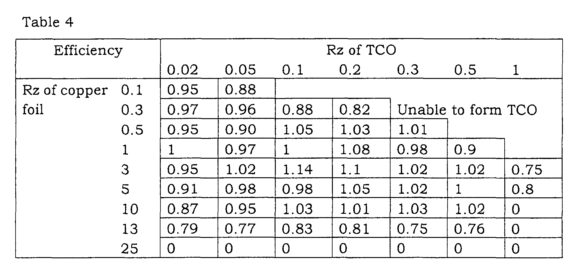
- Table 3 shows the yields when the copper foil has different rough shapes to be formed on the surface, and the mean roughness depth of the rough shapes to be formed on the surface of the transparent conductive material layer is varied by changing etching conditions.
- Zinc oxide (ZnO) is used as the transparent conductive material (TCO).
- the mean roughness depth (Rz) of the rough shape formed on the surface metal foil is required to be approximately 0.1-10 ⁇ m, and the mean roughness depth (Rz) of the rough shape formed on the surface of the transparent conductive material (TCO) layer is required to be 0.02-0.5 ⁇ m as shown in Table 3.
- the substrates used has the copper foils having rough shapes of various mean roughness depth of 0.1-10 ⁇ m, and the transparent conductive material (TCO) layer has rough shapes of various mean roughness depth.
- TCO transparent conductive material
- Table 4 shows standardized characteristics of the thin film solar cell using a substrate of the glass coated with tin oxide (SnO 2 ) having the rough shape.
- the mean roughness depth of the rough shape of the metal foil is preferred to be 0.1-10 ⁇ m, and of the transparent conductive material (TCO) layer is preferred to be 0.02-0.5 ⁇ m.
- Table 4 shows that the mean roughness depth of the rough shape of the metal foil is further preferred to be 3-10 ⁇ m, and of the transparent conductive material (TCO) is further preferred to be 0.1-0.5 ⁇ m.
- a method for integrating the solar cell devices of the structures shown in Figs. 1-3 by referring to Fig. 7 follows.
- the thin film solar cell device 10 having the structure shown in either of Figs. 1-3 is formed, and the rough metal foil substrate 1 and the transparent electrode layer 4 are connected by a connection tab 11 having good conductivity.
- a plurality of the thin film solar cell devices 10 connected with each other are arranged so that a side of the transparent electrode layer 4 is positioned on a front surface glass side.
- the plurality of the thin film solar cell devices 10 are sealed between the front surface glass 12 and a rear surface film 14 with sealing resin 13 of such as EVA (ethylene vinyl acetate) to integrate the cell devices.
- EVA ethylene vinyl acetate
- FIG. 8 is a cross sectional view illustrating a structure of the thin film solar cell of the fourth embodiment according to this invention.
- a plurality of photovoltaic conversion elements are provided on a substrate 1 and these elements are connected and integrated to form an integration type solar cell device.
- an insulative resin layer 15 of such as polyimide is formed on the rough metal foil substrate 1 and the transparent conductive material 16 is formed. Then, the transparent conductive material layer 16 is selectively patterned by YAG laser, SHG laser, excimer layer or the like.
- a photovoltaic conversion layer 17 of a thin film semiconductor having n-i-p junction as in the first embodiment is formed on the transparent conductive material layer 16. Then, the photovoltaic conversion layer 17 is selectively patterned.
- a transparent electrode layer 18 is formed on the photovoltaic conversion layer 17 and is selectively patterned to integrate the cells.
- the thin film solar cell device produced in this embodiment can obtain approximately the same conversion efficiency as that of the substrate of the glass coated with transparent conductive material layer such as tin oxide (SnO 2 ), indium tin oxide (ITO), and zinc oxide (ZnO) having the rough shape which is used conventionally.
- transparent conductive material layer such as tin oxide (SnO 2 ), indium tin oxide (ITO), and zinc oxide (ZnO) having the rough shape which is used conventionally.
- a thin metal layer of relatively high reflectivity formed of such as aluminum and silver may be deposited on the rough metal foil substrate 1 or on the insulative resin layer 15 before forming the transparent conductive material layer 16 so as to improve optical reflectivity.
- the transparent conductive material layer 16 of such as tin oxide, indium tin oxide, and zinc oxide having a fine rough shape may be formed on the metal foil substrate 1. With this shape of the transparent conductive material layer 16, incident light such as sunlight can be effectively utilized and efficiency of the solar cell improves.
- the thin film solar cell device of these embodiment is an amorphous silicon based thin film solar cell device
- this invention may be applicable to thin film solar cell devices of a compound semiconductor based thin film solar cell device, a thin film polycrystalline silicon solar cell device or the like.
- this invention can provide a solar cell device for power generation capable of reducing cost for manufacture because through put in forming a rough shape, and cost for the rough-shaped metal foil substrate itself is less as compared with a substrate of a glass coated with the transparent conductive material of such as tin oxide, indium tin oxide, and zinc oxide.
- the thin film solar cell device using the rough-shaped substrate formed of a metal foil is light-weighted. Therefore, even when the size of the solar cell module increases, the weight is relatively small and workability is good.
Landscapes
- Photovoltaic Devices (AREA)
Abstract
Description
| Reaction gas | Radio frequency power density (mW/cm2) | Substrate temperature (°C) | Reaction pressure (Pa) | |
| n-type layer | PH3:SiH4:H2 = 0.1:10:20 | 30 | 200 | 26.6 |
| i-type layer | H2:SiH4 = 4:1 | 45 | 200 | 26.6 |
| p-type layer | B2H6:CH4:H2:SiH4 = 0.1:5:20:10 | 45 | 100 | 39.9 |
| Voc | Isc | F.F. | Vop | lop | Rs | | η | Yield | ||
| 1st embodiment | 0.99 | 0.95 | 1.0 | 1.0 | 0.89 | 1.56 | 1.37 | 0.94 | 0.93 | |
| 2nd embodiment | 1.01 | 0.99 | 1.01 | 1.02 | 0.99 | 0.88 | 1.01 | 1.01 | 1.02 | |
| 3rd embodiment | 1.02 | 1.19 | 0.94 | 0.98 | 1.13 | 0.97 | 0.43 | 1.14 | 1.0 | |
| Conventional glass / rough-shaped SnO2 substrate | 1.0 | 1.0 | 1.0 | 1.0 | 1.0 | 1.0 | 1.0 | 1.0 | 1.0 | |
| Rolled SUS304 substrate | 0.0 | 0.9 | 0.0 | 0.0 | 0.9 | 0.0 | 0.0 | 0.0 | 0.0 |

Claims (6)
- A solar cell device comprisinga metal foil formed by electroforming,a photovoltaic layer of a thin film semiconductor layer having semiconductor junction in an inside formed on the metal foil.
- The solar cell device according to claim 1,
wherein the metal foil formed by electroforming has a rough shape of approximately 0.1-10 µm of mean roughness depth (Rz) on a surface of the metal foil. - The solar cell device according to claim 1,
wherein the metal foil formed by electroforming has a rough shape of approximately 0.1-5 µm of mean roughness depth (Rz) on a surface of the metal foil. - The solar cell device according to claims 1-3,
wherein a transparent conductive material layer is interposed between the metal foil and the thin film semiconductor layer. - The solar cell device according to claims 1-3,
wherein a conductive material layer of high optical reflectivity and the transparent conductive material layer are interposed between the metal foil and the thin film semiconductor layer. - The solar cell device according to claim 4 or 5,
wherein a rough shape of approximately 0.02-0.5 µm of mean roughness depth (Rz) is formed on a surface of the transparent conductive material layer.
Applications Claiming Priority (4)
| Application Number | Priority Date | Filing Date | Title |
|---|---|---|---|
| JP2000091283 | 2000-03-29 | ||
| JP2000091283 | 2000-03-29 | ||
| JP2001069015 | 2001-03-12 | ||
| JP2001069015A JP2001345460A (en) | 2000-03-29 | 2001-03-12 | Solar cell device |
Publications (2)
| Publication Number | Publication Date |
|---|---|
| EP1139436A2 true EP1139436A2 (en) | 2001-10-04 |
| EP1139436A3 EP1139436A3 (en) | 2006-05-17 |
Family
ID=26588716
Family Applications (1)
| Application Number | Title | Priority Date | Filing Date |
|---|---|---|---|
| EP01107699A Withdrawn EP1139436A3 (en) | 2000-03-29 | 2001-03-28 | Solar cell device |
Country Status (3)
| Country | Link |
|---|---|
| US (1) | US6593522B2 (en) |
| EP (1) | EP1139436A3 (en) |
| JP (1) | JP2001345460A (en) |
Cited By (2)
| Publication number | Priority date | Publication date | Assignee | Title |
|---|---|---|---|---|
| WO2011098255A3 (en) * | 2010-02-11 | 2012-06-28 | Wieland-Werke Ag | Photovoltaic module having a photoactive layer or solar collector having an solar absorber |
| EP2579686A4 (en) * | 2010-06-04 | 2014-12-31 | Mitsui Mining & Smelting Co | ELECTRODE SHEET AND ORGANIC DEVICE |
Families Citing this family (36)
| Publication number | Priority date | Publication date | Assignee | Title |
|---|---|---|---|---|
| JPH0936608A (en) * | 1995-07-13 | 1997-02-07 | Tokin Corp | High frequency electronic parts using coaxial dielectric resonator |
| US6787692B2 (en) * | 2000-10-31 | 2004-09-07 | National Institute Of Advanced Industrial Science & Technology | Solar cell substrate, thin-film solar cell, and multi-junction thin-film solar cell |
| US6750394B2 (en) * | 2001-01-12 | 2004-06-15 | Sharp Kabushiki Kaisha | Thin-film solar cell and its manufacturing method |
| WO2003087564A1 (en) | 2002-04-11 | 2003-10-23 | Haase Richard A | Water combustion technology-methods, processes, systems and apparatus for the combustion of hydrogen and oxygen |
| US7259323B2 (en) * | 2003-04-22 | 2007-08-21 | The Aerospace Corporation | Thin film solar cell thermal radiator |
| DE102004032810B4 (en) * | 2004-07-07 | 2009-01-08 | Saint-Gobain Glass Deutschland Gmbh | Photovoltaic solar cell with a layer of light-scattering properties and solar module |
| US7284471B2 (en) * | 2004-12-02 | 2007-10-23 | Sarcos Investments Lc | Pressure control valve having intrinsic mechanical feedback system |
| US7308848B2 (en) * | 2004-12-02 | 2007-12-18 | Sarcos Investments Lc | Pressure control valve having intrinsic feedback system |
| US7955889B1 (en) * | 2006-07-11 | 2011-06-07 | The Trustees Of Princeton University | Organic photosensitive cells grown on rough electrode with nano-scale morphology control |
| TWI349371B (en) * | 2007-02-13 | 2011-09-21 | Epistar Corp | An optoelectronical semiconductor device having a bonding structure |
| KR101081706B1 (en) * | 2007-05-09 | 2011-11-09 | 히다치 가세고교 가부시끼가이샤 | Method for connecting conductor, member for connecting conductor, connecting structure and solar cell module |
| JP5115553B2 (en) * | 2007-05-09 | 2013-01-09 | 日立化成工業株式会社 | Conductor connection member, connection structure, and solar cell module |
| JP4304638B2 (en) | 2007-07-13 | 2009-07-29 | オムロン株式会社 | CIS solar cell and manufacturing method thereof |
| JP5299648B2 (en) * | 2008-10-29 | 2013-09-25 | 三菱瓦斯化学株式会社 | Textile processing liquid for transparent conductive film mainly composed of zinc oxide and method for producing transparent conductive film having irregularities |
| US20100132783A1 (en) * | 2008-12-02 | 2010-06-03 | Applied Materials, Inc. | Transparent conductive film with high surface roughness formed by a reactive sputter deposition |
| US8486282B2 (en) * | 2009-03-25 | 2013-07-16 | Intermolecular, Inc. | Acid chemistries and methodologies for texturing transparent conductive oxide materials |
| TW201044601A (en) * | 2009-06-08 | 2010-12-16 | Univ Nat Chiao Tung | Three-dimensional indium-tin-oxide electrode, method of fabricating the same, device of fabricating the same, and method of fabricating solar cell comprising the same |
| JP5537101B2 (en) * | 2009-09-10 | 2014-07-02 | 株式会社カネカ | Crystalline silicon solar cell |
| DE102009056128A1 (en) * | 2009-10-27 | 2011-04-28 | Robert Bosch Gmbh | Backsheet system for thin film solar modules, thin film solar module, and method of forming a backsheet system |
| DE102009056129A1 (en) * | 2009-10-27 | 2011-04-28 | Robert Bosch Gmbh | Backsheet system for thin film solar modules, thin film solar module, and method of making a backsheet system for thin film solar modules |
| KR101091405B1 (en) * | 2009-10-28 | 2011-12-07 | 엘지이노텍 주식회사 | Solar cell and manufacturing method thereof |
| US8878055B2 (en) * | 2010-08-09 | 2014-11-04 | International Business Machines Corporation | Efficient nanoscale solar cell and fabrication method |
| JP5269014B2 (en) * | 2010-09-08 | 2013-08-21 | 三洋電機株式会社 | Solar cell module |
| CN103155725B (en) * | 2010-10-22 | 2016-07-06 | 索尼公司 | Pattern substrate, the manufacture method of pattern substrate, message input device and display device |
| JP2011044750A (en) * | 2010-11-30 | 2011-03-03 | Sanyo Electric Co Ltd | Solar cell module |
| JP5884077B2 (en) * | 2010-12-29 | 2016-03-15 | パナソニックIpマネジメント株式会社 | Solar cell and solar cell module |
| CN103299433A (en) * | 2011-01-12 | 2013-09-11 | 株式会社新王材料 | Metal substrate for solar cell and method for producing metal substrate for solar cell |
| KR101259296B1 (en) * | 2011-06-13 | 2013-05-06 | 주식회사 포스코 | Fe-Ni ALLOY SUBSTRATE FOR SOLAR CELL AND METHOD FOR MANUFACTURING THE SAME, AND SOLLAR CELL USING THE SAME |
| US8628996B2 (en) | 2011-06-15 | 2014-01-14 | International Business Machines Corporation | Uniformly distributed self-assembled cone-shaped pillars for high efficiency solar cells |
| KR101422609B1 (en) * | 2011-11-17 | 2014-07-24 | 한국생산기술연구원 | Thermal Expansion Control Type Flexible Metal Substrate With Texture |
| JP5950154B2 (en) * | 2012-05-09 | 2016-07-13 | パナソニックIpマネジメント株式会社 | Solar cell module |
| US8889456B2 (en) | 2012-08-29 | 2014-11-18 | International Business Machines Corporation | Method of fabricating uniformly distributed self-assembled solder dot formation for high efficiency solar cells |
| JP6141641B2 (en) | 2013-01-09 | 2017-06-07 | 三井金属鉱業株式会社 | Electrolytic copper foil and electronic device |
| KR20150039536A (en) | 2013-10-02 | 2015-04-10 | 엘지이노텍 주식회사 | Solar cell |
| DE102016113002B4 (en) * | 2016-07-14 | 2022-09-29 | OSRAM Opto Semiconductors Gesellschaft mit beschränkter Haftung | Devices with improved efficiency and methods of manufacturing devices |
| GB201709562D0 (en) * | 2017-06-15 | 2017-08-02 | Grafmarine | Power distrubution and cell storage apparatus |
Family Cites Families (14)
| Publication number | Priority date | Publication date | Assignee | Title |
|---|---|---|---|---|
| US4328390A (en) * | 1979-09-17 | 1982-05-04 | The University Of Delaware | Thin film photovoltaic cell |
| US4419533A (en) * | 1982-03-03 | 1983-12-06 | Energy Conversion Devices, Inc. | Photovoltaic device having incident radiation directing means for total internal reflection |
| JPS59108370A (en) * | 1982-12-14 | 1984-06-22 | Kanegafuchi Chem Ind Co Ltd | Photovoltaic device |
| US4530739A (en) * | 1984-03-09 | 1985-07-23 | Energy Conversion Devices, Inc. | Method of fabricating an electroplated substrate |
| JP2908067B2 (en) * | 1991-05-09 | 1999-06-21 | キヤノン株式会社 | Substrate for solar cell and solar cell |
| US5221854A (en) * | 1991-11-18 | 1993-06-22 | United Solar Systems Corporation | Protective layer for the back reflector of a photovoltaic device |
| US5656098A (en) * | 1992-03-03 | 1997-08-12 | Canon Kabushiki Kaisha | Photovoltaic conversion device and method for producing same |
| JP3651932B2 (en) * | 1994-08-24 | 2005-05-25 | キヤノン株式会社 | Back surface reflective layer for photovoltaic device, method for forming the same, photovoltaic device and method for manufacturing the same |
| EP0793277B1 (en) * | 1996-02-27 | 2001-08-22 | Canon Kabushiki Kaisha | Photovoltaic device provided with an opaque substrate having a specific irregular surface structure |
| JP2984595B2 (en) * | 1996-03-01 | 1999-11-29 | キヤノン株式会社 | Photovoltaic element |
| US6172296B1 (en) * | 1996-05-17 | 2001-01-09 | Canon Kabushiki Kaisha | Photovoltaic cell |
| US6512170B1 (en) * | 2000-03-02 | 2003-01-28 | Nippon Sheet Glass Co., Ltd. | Photoelectric conversion device |
| JP4171162B2 (en) * | 2000-05-30 | 2008-10-22 | 三洋電機株式会社 | Photovoltaic element and manufacturing method thereof |
| US6787692B2 (en) * | 2000-10-31 | 2004-09-07 | National Institute Of Advanced Industrial Science & Technology | Solar cell substrate, thin-film solar cell, and multi-junction thin-film solar cell |
-
2001
- 2001-03-12 JP JP2001069015A patent/JP2001345460A/en active Pending
- 2001-03-27 US US09/817,202 patent/US6593522B2/en not_active Expired - Lifetime
- 2001-03-28 EP EP01107699A patent/EP1139436A3/en not_active Withdrawn
Cited By (3)
| Publication number | Priority date | Publication date | Assignee | Title |
|---|---|---|---|---|
| WO2011098255A3 (en) * | 2010-02-11 | 2012-06-28 | Wieland-Werke Ag | Photovoltaic module having a photoactive layer or solar collector having an solar absorber |
| EP2579686A4 (en) * | 2010-06-04 | 2014-12-31 | Mitsui Mining & Smelting Co | ELECTRODE SHEET AND ORGANIC DEVICE |
| US9490440B2 (en) | 2010-06-04 | 2016-11-08 | Mitsui Mining & Smelting Co., Ltd. | Electrode foil and organic device |
Also Published As
| Publication number | Publication date |
|---|---|
| US6593522B2 (en) | 2003-07-15 |
| JP2001345460A (en) | 2001-12-14 |
| US20010037825A1 (en) | 2001-11-08 |
| EP1139436A3 (en) | 2006-05-17 |
Similar Documents
| Publication | Publication Date | Title |
|---|---|---|
| US6593522B2 (en) | Solar cell device | |
| US6123824A (en) | Process for producing photo-electricity generating device | |
| US6613973B2 (en) | Photovoltaic element, producing method therefor, and solar cell modules | |
| JP2686022B2 (en) | Method for manufacturing photovoltaic element | |
| JP3327811B2 (en) | Method for producing zinc oxide thin film, photovoltaic element and semiconductor element substrate using the same | |
| US20030230338A1 (en) | Thin film solar cell configuration and fabrication method | |
| KR100334595B1 (en) | Manufacturing method of photovoltaic device | |
| JPH04266068A (en) | Photoelectric conversion element and its manufacture | |
| KR20000048653A (en) | Method of manufacturing a photovoltaic foil | |
| JPH05243596A (en) | Manufacture of laminated type solar cell | |
| JP3801342B2 (en) | Solar cell substrate, manufacturing method thereof, and semiconductor element | |
| US6951770B2 (en) | Method of manufacturing a photovoltaic foil | |
| JP4240933B2 (en) | Laminate formation method | |
| CN116314370B (en) | A heterojunction solar cell and a method for preparing the same | |
| US9391215B2 (en) | Device for generating photovoltaic power and method for manufacturing same | |
| JP3078936B2 (en) | Solar cell | |
| CN121335289A (en) | A composite seed layer and copper grid heterojunction solar cell | |
| WO2023071168A1 (en) | Solar cell and preparation method therefor | |
| JP3618986B2 (en) | Photovoltaic element manufacturing method | |
| JPH0864850A (en) | Thin film solar cell and method of manufacturing the same | |
| JP4966525B2 (en) | Dye-sensitized solar cell, its photoelectrode substrate, and method for producing the photoelectrode substrate | |
| US20240224550A1 (en) | Solar cell | |
| JP2006080371A (en) | Solar cell and manufacturing method thereof | |
| JP2010239055A (en) | Solar cell using surface roughened copper plate | |
| JP2003008036A (en) | Solar cell and method of manufacturing the same |
Legal Events
| Date | Code | Title | Description |
|---|---|---|---|
| PUAI | Public reference made under article 153(3) epc to a published international application that has entered the european phase |
Free format text: ORIGINAL CODE: 0009012 |
|
| AK | Designated contracting states |
Kind code of ref document: A2 Designated state(s): AT BE CH CY DE DK ES FI FR GB GR IE IT LI LU MC NL PT SE TR |
|
| AX | Request for extension of the european patent |
Free format text: AL;LT;LV;MK;RO;SI |
|
| PUAL | Search report despatched |
Free format text: ORIGINAL CODE: 0009013 |
|
| AK | Designated contracting states |
Kind code of ref document: A3 Designated state(s): AT BE CH CY DE DK ES FI FR GB GR IE IT LI LU MC NL PT SE TR |
|
| AX | Request for extension of the european patent |
Extension state: AL LT LV MK RO SI |
|
| 17P | Request for examination filed |
Effective date: 20060717 |
|
| AKX | Designation fees paid |
Designated state(s): DE FR IT |
|
| 17Q | First examination report despatched |
Effective date: 20070212 |
|
| STAA | Information on the status of an ep patent application or granted ep patent |
Free format text: STATUS: THE APPLICATION IS DEEMED TO BE WITHDRAWN |
|
| 18D | Application deemed to be withdrawn |
Effective date: 20151215 |