EP1139435A2 - Chip scale packaging for optical image sensing integrated circuits - Google Patents
Chip scale packaging for optical image sensing integrated circuits Download PDFInfo
- Publication number
- EP1139435A2 EP1139435A2 EP00311102A EP00311102A EP1139435A2 EP 1139435 A2 EP1139435 A2 EP 1139435A2 EP 00311102 A EP00311102 A EP 00311102A EP 00311102 A EP00311102 A EP 00311102A EP 1139435 A2 EP1139435 A2 EP 1139435A2
- Authority
- EP
- European Patent Office
- Prior art keywords
- wafer
- adhesive matrix
- adhesive
- cover glass
- micro lenses
- Prior art date
- Legal status (The legal status is an assumption and is not a legal conclusion. Google has not performed a legal analysis and makes no representation as to the accuracy of the status listed.)
- Granted
Links
Images

Classifications
-
- H—ELECTRICITY
- H10—SEMICONDUCTOR DEVICES; ELECTRIC SOLID-STATE DEVICES NOT OTHERWISE PROVIDED FOR
- H10F—INORGANIC SEMICONDUCTOR DEVICES SENSITIVE TO INFRARED RADIATION, LIGHT, ELECTROMAGNETIC RADIATION OF SHORTER WAVELENGTH OR CORPUSCULAR RADIATION
- H10F77/00—Constructional details of devices covered by this subclass
- H10F77/50—Encapsulations or containers
-
- H—ELECTRICITY
- H10—SEMICONDUCTOR DEVICES; ELECTRIC SOLID-STATE DEVICES NOT OTHERWISE PROVIDED FOR
- H10F—INORGANIC SEMICONDUCTOR DEVICES SENSITIVE TO INFRARED RADIATION, LIGHT, ELECTROMAGNETIC RADIATION OF SHORTER WAVELENGTH OR CORPUSCULAR RADIATION
- H10F39/00—Integrated devices, or assemblies of multiple devices, comprising at least one element covered by group H10F30/00, e.g. radiation detectors comprising photodiode arrays
- H10F39/80—Constructional details of image sensors
- H10F39/804—Containers or encapsulations
Definitions
- the present invention is related to image sensing integrated circuits, and more particularly, to a method for chip scale packaging using an adhesive matrix.
- optically clear adhesive can be an epoxy and the transparent material is glass.
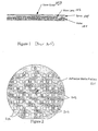
- a typical chip scale package for an imaging sensor is shown.
- the packaging technique includes a wafer 101 having the image sensor chips formed thereon.
- Micro lenses 103 are formed atop of the wafer 101 to cover each pixel (picture element) individually.
- an adhesive layer 105 is then applied, typically using some type of homogenous spin coating technique.
- a cover glass 107 is applied to the adhesive.
- the adhesive 105 serves to secure the cover glass 107 to the wafer 101.
- the adhesive 105 is an epoxy.
- the backside of the wafer 101 is ground down to make the wafer thinner.
- a wafer sawing operation is used to expose the extended image sensor electrical leads though the back side of the thinned wafer.
- the exposed leads are then extended to form electrical contacts with traditional deposition and etching processes.
- a die cutting machine is used to cut the wafer 101 into individual image sensors.
- the present invention is a chip scale packaging method for optical image sensor integrated circuits.
- Micro lenses are placed on top of a wafer having the image sensors formed thereon.
- An adhesive matrix such as epoxy is placed atop of the wafer.
- the matrix has openings that align with the image-sensing array of the integrated circuit on top of the wafer.
- a cover glass is then placed over the matrix and the adhesive is activated to secure the cover glass to the wafer. Because the adhesive has openings above the micro lenses, no distortion is caused by the adhesive.
- Figure 1 is a prior art chip scale packaging technique for image sensor integrated circuits.
- Figure 2 is a top view of a matrix formed in accordance with the present invention.
- Figure 3 is a cross-sectional view of a chip scale packaging for image sensors formed in accordance with the present invention.
- Figure 4 is a top view of the chip scale packaging shown in Fig. 3.
- an adhesive matrix is used to adhere a cover glass to a wafer having image sensors formed thereon.
- an adhesive matrix 201 is provided.
- the adhesive matrix 201 is also referred to as a preform.
- the adhesive matrix 201 includes openings 203.
- the openings 203 are formed to coincide with the locations on a wafer that contain micro lenses.
- the openings 203 are aligned with and are placed atop of the micro lenses 303 formed atop of a wafer 301.
- the adhesive matrix 201 is laid atop of the wafer 301, the openings 203 are aligned with the micro lenses 303.
- a cover glass 307 is applied atop of the adhesive matrix 201.
- the adhesive matrix 201 has substantially the same size as the wafer 301.
- the adhesive matrix 201 is activated by the application of light, pressure and/or heat. This causes the adhesive matrix 201 to secure the cover glass 307 to the wafer 301.
- cavities 309 are formed between the cover glass 307 and the micro lensed array 303.
- a top view of the chip package is shown in Fig. 4.
- the outer boundaries of the image sensor are shown by reference numeral 401.
- the lensed array 303 only covers a portion of the actual integrated circuit 401.
- the balance of the integrated circuit 401 is used for signal processing, and thus, is not covered by micro lenses 303.
- the peripheral region of the integrated circuit 401 can be covered by the adhesive of the adhesive matrix 201 without adverse effect.
- the wafer 301 can be further processed and sliced to generate individual integrated circuit devices.
- the cavities 309 formed by the use of the adhesive matrix 201 can be realized.
- the cavities 309 may be filled with gaseous or liquid materials that further enhance the optical properties, temperature characteristics, or other performance characteristics of the imaging sensor.
- the filling of the cavity with gas or liquid material would precede the application of the cover glass 307.
- a gaseous or liquid material that has a refractive index of less than one would further enhance the optical property of the micro lenses.
- a gaseous or liquid material that has good heat dissipating properties may be used to dissipate heat generated by the imaging sensor, thereby increasing the performance characteristics of the image device.
- the adhesive material may be made opaque to enhance device performance
- the adhesive matrix 201 may be of varying size to match the size of the wafer 301.
- the openings 203 can be of varying size to correlate with the sizes of the micro lensed array incorporated into the image sensors formed on the wafer 301.
- the adhesive may be applied in the required pattern with liquid dispensing equipment, or with techniques similar to screen printing.
Landscapes
- Solid State Image Pick-Up Elements (AREA)
- Transforming Light Signals Into Electric Signals (AREA)
Abstract
Description
- The present invention is related to image sensing integrated circuits, and more particularly, to a method for chip scale packaging using an adhesive matrix.
- Currently, prior art chip scale packaging for optical image sensor devices require that a wafer be completely coated with an optically clear adhesive and subsequently covered with a transparent covering material. Typically, the optically clear adhesive can be an epoxy and the transparent material is glass.
- However, nearly all image sensors require the application of micro lenses to increase the optical fill factor to meet performance objectives. As seen in Fig. 1, a typical chip scale package for an imaging sensor is shown. The packaging technique includes a
wafer 101 having the image sensor chips formed thereon.Micro lenses 103 are formed atop of thewafer 101 to cover each pixel (picture element) individually. After pads have been extended into the scribe lines, anadhesive layer 105 is then applied, typically using some type of homogenous spin coating technique. Finally, a cover glass 107 is applied to the adhesive. The adhesive 105 serves to secure the cover glass 107 to thewafer 101. Typically, theadhesive 105 is an epoxy. - Next, the backside of the
wafer 101 is ground down to make the wafer thinner. Next a wafer sawing operation is used to expose the extended image sensor electrical leads though the back side of the thinned wafer. The exposed leads are then extended to form electrical contacts with traditional deposition and etching processes. Finally, a die cutting machine is used to cut thewafer 101 into individual image sensors. - However, this prior art method of chip scale packaging is problematical for image sensors because the refractive index of the micro lens material is very similar to the
adhesive 105. Thus, theadhesive 105 tends to counteract the optical effect of themicro lenses 103. - The present invention is a chip scale packaging method for optical image sensor integrated circuits. Micro lenses are placed on top of a wafer having the image sensors formed thereon. An adhesive matrix such as epoxy is placed atop of the wafer. The matrix has openings that align with the image-sensing array of the integrated circuit on top of the wafer. A cover glass is then placed over the matrix and the adhesive is activated to secure the cover glass to the wafer. Because the adhesive has openings above the micro lenses, no distortion is caused by the adhesive.
- Figure 1 is a prior art chip scale packaging technique for image sensor integrated circuits.
- Figure 2 is a top view of a matrix formed in accordance with the present invention.
- Figure 3 is a cross-sectional view of a chip scale packaging for image sensors formed in accordance with the present invention.
- Figure 4 is a top view of the chip scale packaging shown in Fig. 3.
- In accordance with the present invention, an adhesive matrix is used to adhere a cover glass to a wafer having image sensors formed thereon. Specifically, turning to Fig. 2, an
adhesive matrix 201 is provided. Theadhesive matrix 201 is also referred to as a preform. Theadhesive matrix 201 includesopenings 203. Theopenings 203 are formed to coincide with the locations on a wafer that contain micro lenses. - Thus, as seen in Fig. 4, the
openings 203 are aligned with and are placed atop of themicro lenses 303 formed atop of awafer 301. When theadhesive matrix 201 is laid atop of thewafer 301, theopenings 203 are aligned with themicro lenses 303. Next, acover glass 307 is applied atop of theadhesive matrix 201. Note that theadhesive matrix 201 has substantially the same size as thewafer 301. After thecover glass 307 is placed atop of theadhesive matrix 201, theadhesive matrix 201 is activated by the application of light, pressure and/or heat. This causes theadhesive matrix 201 to secure thecover glass 307 to thewafer 301. The result is thatcavities 309 are formed between thecover glass 307 and the microlensed array 303. A top view of the chip package is shown in Fig. 4. - Additionally, as seen in Fig. 4, the outer boundaries of the image sensor are shown by
reference numeral 401. Note that thelensed array 303 only covers a portion of the actualintegrated circuit 401. The balance of the integratedcircuit 401 is used for signal processing, and thus, is not covered bymicro lenses 303. The peripheral region of the integratedcircuit 401 can be covered by the adhesive of theadhesive matrix 201 without adverse effect. Following the adhesion of thecover glass 307 to thewafer 301, in accordance with the prior art, thewafer 301 can be further processed and sliced to generate individual integrated circuit devices. - By having an adhesive matrix having openings that do not cover the micro lensed sensing array, the problems of the prior art with the epoxy counteracting the effect of the micro lenses is avoided. In other words, a cavity that does not contain adhesive is formed over the micro lenses. This allows the micro lenses to perform their function without interference by the adhesive .
- Indeed, other benefits from the
cavities 309 formed by the use of theadhesive matrix 201 can be realized. For example, thecavities 309 may be filled with gaseous or liquid materials that further enhance the optical properties, temperature characteristics, or other performance characteristics of the imaging sensor. The filling of the cavity with gas or liquid material would precede the application of thecover glass 307. For example, a gaseous or liquid material that has a refractive index of less than one would further enhance the optical property of the micro lenses. Additionally, a gaseous or liquid material that has good heat dissipating properties may be used to dissipate heat generated by the imaging sensor, thereby increasing the performance characteristics of the image device. Finally, the adhesive material may be made opaque to enhance device performance - The above description of illustrated embodiments of the invention is not intended to be exhaustive or to limit the invention to the precise forms disclosed. While specific embodiments of, and examples for, the invention are described herein for illustrative purposes, various equivalent modifications are possible within the scope of the invention, as those skilled in the relevant art will recognize. For example, the
adhesive matrix 201 may be of varying size to match the size of thewafer 301. In addition, theopenings 203 can be of varying size to correlate with the sizes of the micro lensed array incorporated into the image sensors formed on thewafer 301. These modifications can be made to the invention in light of the above detailed description. The terms used in the following claims should not be construed to limit the invention to the specific embodiments disclosed in the specification and the claims. Rather, the scope of the invention is to be determined entirely by the following claims that are to be construed with accordance with established doctrines of claim interpretation. - For example, instead of using an adhesive preform to form the cavities, the adhesive may be applied in the required pattern with liquid dispensing equipment, or with techniques similar to screen printing.
Claims (4)
- A method comprising:applying micro lenses onto a wafer, said wafer including a plurality of image sensor integrated circuits, said micro lenses being applied to a sensing array portion of said image sensor integrated circuits;applying an adhesive matrix atop of said wafer, said adhesive matrix including a plurality of openings located to correspond to said sensing array portion when said adhesive matrix is applied to said wafer; andapplying a cover glass atop of said adhesive matrix.
- The method of Claim 1 further including the step of activating said adhesive matrix to bind said cover glass to said wafer.
- A chip scale package comprising:a wafer containing a plurality of image sensor integrated circuits, said wafer having micro lenses applied thereto, one set of micro lenses for each image sensor integrated circuit;an adhesive matrix applied to said wafer, said adhesive matrix having openings corresponding to the locations of said micro lenses; anda cover glass applied to said adhesive matrix, said adhesive matrix securing said cover glass to said wafer.
- A chip scale package comprising:a wafer containing a plurality of image sensors, each image sensor having a sensing area, said wafer having micro lenses applied thereto, one set of micro lenses for each image sensor;an adhesive matrix applied to said wafer, said adhesive matrix having openings corresponding to the locations of said sensing areas; anda cover glass applied to said adhesive matrix, said adhesive matrix securing said cover glass to said wafer.
Applications Claiming Priority (2)
| Application Number | Priority Date | Filing Date | Title |
|---|---|---|---|
| US09/536,890 US6285064B1 (en) | 2000-03-28 | 2000-03-28 | Chip scale packaging technique for optical image sensing integrated circuits |
| US536890 | 2000-03-28 |
Publications (3)
| Publication Number | Publication Date |
|---|---|
| EP1139435A2 true EP1139435A2 (en) | 2001-10-04 |
| EP1139435A3 EP1139435A3 (en) | 2004-08-11 |
| EP1139435B1 EP1139435B1 (en) | 2011-06-15 |
Family
ID=24140345
Family Applications (1)
| Application Number | Title | Priority Date | Filing Date |
|---|---|---|---|
| EP00311102A Expired - Lifetime EP1139435B1 (en) | 2000-03-28 | 2000-12-13 | Chip scale packaging method for optical image sensor integrated circuits |
Country Status (4)
| Country | Link |
|---|---|
| US (1) | US6285064B1 (en) |
| EP (1) | EP1139435B1 (en) |
| CN (1) | CN1182588C (en) |
| TW (1) | TW465054B (en) |
Cited By (1)
| Publication number | Priority date | Publication date | Assignee | Title |
|---|---|---|---|---|
| KR100640957B1 (en) | 2004-12-30 | 2006-11-02 | 동부일렉트로닉스 주식회사 | Image sensor wafer transport mechanism |
Families Citing this family (94)
| Publication number | Priority date | Publication date | Assignee | Title |
|---|---|---|---|---|
| IL133453A0 (en) * | 1999-12-10 | 2001-04-30 | Shellcase Ltd | Methods for producing packaged integrated circuit devices and packaged integrated circuit devices produced thereby |
| US6287891B1 (en) * | 2000-04-05 | 2001-09-11 | Hrl Laboratories, Llc | Method for transferring semiconductor device layers to different substrates |
| US6856007B2 (en) | 2001-08-28 | 2005-02-15 | Tessera, Inc. | High-frequency chip packages |
| KR20050043754A (en) * | 2001-11-05 | 2005-05-11 | 미츠마사 코야나기 | Solid-state image sensor and its production method |
| JP4472340B2 (en) | 2001-11-05 | 2010-06-02 | 株式会社ザイキューブ | Semiconductor device using low dielectric constant material film and manufacturing method thereof |
| JP2003163342A (en) * | 2001-11-29 | 2003-06-06 | Olympus Optical Co Ltd | Solid-state imaging device and manufacturing method thereof |
| US6936495B1 (en) | 2002-01-09 | 2005-08-30 | Bridge Semiconductor Corporation | Method of making an optoelectronic semiconductor package device |
| US6891276B1 (en) | 2002-01-09 | 2005-05-10 | Bridge Semiconductor Corporation | Semiconductor package device |
| JP2003244560A (en) * | 2002-02-21 | 2003-08-29 | Seiko Precision Inc | Solid-state image pickup device |
| US6908791B2 (en) * | 2002-04-29 | 2005-06-21 | Texas Instruments Incorporated | MEMS device wafer-level package |
| US6906403B2 (en) | 2002-06-04 | 2005-06-14 | Micron Technology, Inc. | Sealed electronic device packages with transparent coverings |
| US6744109B2 (en) * | 2002-06-26 | 2004-06-01 | Agilent Technologies, Inc. | Glass attachment over micro-lens arrays |
| US7414661B2 (en) * | 2002-08-13 | 2008-08-19 | Micron Technology, Inc. | CMOS image sensor using gradient index chip scale lenses |
| US20040038442A1 (en) * | 2002-08-26 | 2004-02-26 | Kinsman Larry D. | Optically interactive device packages and methods of assembly |
| JP4397819B2 (en) | 2002-09-17 | 2010-01-13 | アンテルヨン、ベスローテン、フェンノートシャップ | CAMERA DEVICE AND METHOD FOR MANUFACTURING CAMERA DEVICE AND WAFER SCALE PACKAGE |
| US7033664B2 (en) | 2002-10-22 | 2006-04-25 | Tessera Technologies Hungary Kft | Methods for producing packaged integrated circuit devices and packaged integrated circuit devices produced thereby |
| US6900531B2 (en) * | 2002-10-25 | 2005-05-31 | Freescale Semiconductor, Inc. | Image sensor device |
| ITMI20022467A1 (en) * | 2002-11-20 | 2004-05-21 | St Microelectronics Srl | PROCESS FOR REALIZING A BYTE SELECTION TRANSISTOR FOR |
| US20040124486A1 (en) * | 2002-12-26 | 2004-07-01 | Katsumi Yamamoto | Image sensor adapted for reduced component chip scale packaging |
| US20040150063A1 (en) * | 2003-01-10 | 2004-08-05 | Katsumi Yamamoto | Package structure for an optical image sensor |
| TWI286434B (en) * | 2003-03-12 | 2007-09-01 | Hon Hai Prec Ind Co Ltd | Digital camera |
| JP2004312666A (en) * | 2003-03-25 | 2004-11-04 | Fuji Photo Film Co Ltd | Solid-state imaging device and method for manufacturing solid-state imaging device |
| US20040226735A1 (en) * | 2003-05-12 | 2004-11-18 | Ping Wu | Method and apparatus for integrated noise decoupling |
| JP4497844B2 (en) * | 2003-05-30 | 2010-07-07 | キヤノン株式会社 | Method for manufacturing solid-state imaging device |
| US6972480B2 (en) | 2003-06-16 | 2005-12-06 | Shellcase Ltd. | Methods and apparatus for packaging integrated circuit devices |
| JP2007528120A (en) | 2003-07-03 | 2007-10-04 | テッセラ テクノロジーズ ハンガリー コルラートルト フェレロェセーギュー タールシャシャーグ | Method and apparatus for packaging integrated circuit devices |
| US20050009239A1 (en) * | 2003-07-07 | 2005-01-13 | Wolff Larry Lee | Optoelectronic packaging with embedded window |
| US6953891B2 (en) * | 2003-09-16 | 2005-10-11 | Micron Technology, Inc. | Moisture-resistant electronic device package and methods of assembly |
| US6995462B2 (en) | 2003-09-17 | 2006-02-07 | Micron Technology, Inc. | Image sensor packages |
| US6934065B2 (en) * | 2003-09-18 | 2005-08-23 | Micron Technology, Inc. | Microelectronic devices and methods for packaging microelectronic devices |
| WO2005031862A1 (en) | 2003-09-26 | 2005-04-07 | Tessera, Inc. | Structure and method of making sealed capped chips |
| US7583862B2 (en) * | 2003-11-26 | 2009-09-01 | Aptina Imaging Corporation | Packaged microelectronic imagers and methods of packaging microelectronic imagers |
| US6905910B1 (en) * | 2004-01-06 | 2005-06-14 | Freescale Semiconductor, Inc. | Method of packaging an optical sensor |
| US7253397B2 (en) * | 2004-02-23 | 2007-08-07 | Micron Technology, Inc. | Packaged microelectronic imagers and methods of packaging microelectronic imagers |
| JP4476764B2 (en) * | 2004-03-26 | 2010-06-09 | 富士フイルム株式会社 | Substrate bonding apparatus and method |
| US8953087B2 (en) * | 2004-04-08 | 2015-02-10 | Flir Systems Trading Belgium Bvba | Camera system and associated methods |
| US8049806B2 (en) * | 2004-09-27 | 2011-11-01 | Digitaloptics Corporation East | Thin camera and associated methods |
| US8092734B2 (en) * | 2004-05-13 | 2012-01-10 | Aptina Imaging Corporation | Covers for microelectronic imagers and methods for wafer-level packaging of microelectronics imagers |
| US7253957B2 (en) * | 2004-05-13 | 2007-08-07 | Micron Technology, Inc. | Integrated optics units and methods of manufacturing integrated optics units for use with microelectronic imagers |
| US20050275750A1 (en) | 2004-06-09 | 2005-12-15 | Salman Akram | Wafer-level packaged microelectronic imagers and processes for wafer-level packaging |
| US7498647B2 (en) | 2004-06-10 | 2009-03-03 | Micron Technology, Inc. | Packaged microelectronic imagers and methods of packaging microelectronic imagers |
| US7199439B2 (en) * | 2004-06-14 | 2007-04-03 | Micron Technology, Inc. | Microelectronic imagers and methods of packaging microelectronic imagers |
| US7262405B2 (en) * | 2004-06-14 | 2007-08-28 | Micron Technology, Inc. | Prefabricated housings for microelectronic imagers |
| US7232754B2 (en) | 2004-06-29 | 2007-06-19 | Micron Technology, Inc. | Microelectronic devices and methods for forming interconnects in microelectronic devices |
| US7294897B2 (en) * | 2004-06-29 | 2007-11-13 | Micron Technology, Inc. | Packaged microelectronic imagers and methods of packaging microelectronic imagers |
| US7416913B2 (en) * | 2004-07-16 | 2008-08-26 | Micron Technology, Inc. | Methods of manufacturing microelectronic imaging units with discrete standoffs |
| US7189954B2 (en) * | 2004-07-19 | 2007-03-13 | Micron Technology, Inc. | Microelectronic imagers with optical devices and methods of manufacturing such microelectronic imagers |
| US7402453B2 (en) * | 2004-07-28 | 2008-07-22 | Micron Technology, Inc. | Microelectronic imaging units and methods of manufacturing microelectronic imaging units |
| US7364934B2 (en) * | 2004-08-10 | 2008-04-29 | Micron Technology, Inc. | Microelectronic imaging units and methods of manufacturing microelectronic imaging units |
| US7645635B2 (en) * | 2004-08-16 | 2010-01-12 | Micron Technology, Inc. | Frame structure and semiconductor attach process for use therewith for fabrication of image sensor packages and the like, and resulting packages |
| US7223626B2 (en) * | 2004-08-19 | 2007-05-29 | Micron Technology, Inc. | Spacers for packaged microelectronic imagers and methods of making and using spacers for wafer-level packaging of imagers |
| US7397066B2 (en) * | 2004-08-19 | 2008-07-08 | Micron Technology, Inc. | Microelectronic imagers with curved image sensors and methods for manufacturing microelectronic imagers |
| US7115961B2 (en) * | 2004-08-24 | 2006-10-03 | Micron Technology, Inc. | Packaged microelectronic imaging devices and methods of packaging microelectronic imaging devices |
| US7429494B2 (en) * | 2004-08-24 | 2008-09-30 | Micron Technology, Inc. | Microelectronic imagers with optical devices having integral reference features and methods for manufacturing such microelectronic imagers |
| US7425499B2 (en) | 2004-08-24 | 2008-09-16 | Micron Technology, Inc. | Methods for forming interconnects in vias and microelectronic workpieces including such interconnects |
| US7276393B2 (en) | 2004-08-26 | 2007-10-02 | Micron Technology, Inc. | Microelectronic imaging units and methods of manufacturing microelectronic imaging units |
| US7511262B2 (en) * | 2004-08-30 | 2009-03-31 | Micron Technology, Inc. | Optical device and assembly for use with imaging dies, and wafer-label imager assembly |
| US20070148807A1 (en) * | 2005-08-22 | 2007-06-28 | Salman Akram | Microelectronic imagers with integrated optical devices and methods for manufacturing such microelectronic imagers |
| US7646075B2 (en) * | 2004-08-31 | 2010-01-12 | Micron Technology, Inc. | Microelectronic imagers having front side contacts |
| US7300857B2 (en) | 2004-09-02 | 2007-11-27 | Micron Technology, Inc. | Through-wafer interconnects for photoimager and memory wafers |
| US7453653B2 (en) | 2004-09-14 | 2008-11-18 | Omnivision Cdm Optics, Inc. | Low height imaging system and associated methods |
| US7253028B2 (en) * | 2004-09-24 | 2007-08-07 | Youngtek Electronics Corp. | Image sensor packaging method and structure thereof |
| KR100498708B1 (en) * | 2004-11-08 | 2005-07-01 | 옵토팩 주식회사 | Electronic package for semiconductor device and packaging method thereof |
| US7271482B2 (en) * | 2004-12-30 | 2007-09-18 | Micron Technology, Inc. | Methods for forming interconnects in microelectronic workpieces and microelectronic workpieces formed using such methods |
| US7273767B2 (en) * | 2004-12-31 | 2007-09-25 | Carsem (M) Sdn. Bhd. | Method of manufacturing a cavity package |
| US7214919B2 (en) * | 2005-02-08 | 2007-05-08 | Micron Technology, Inc. | Microelectronic imaging units and methods of manufacturing microelectronic imaging units |
| US20060177999A1 (en) * | 2005-02-10 | 2006-08-10 | Micron Technology, Inc. | Microelectronic workpieces and methods for forming interconnects in microelectronic workpieces |
| US7303931B2 (en) * | 2005-02-10 | 2007-12-04 | Micron Technology, Inc. | Microfeature workpieces having microlenses and methods of forming microlenses on microfeature workpieces |
| US7190039B2 (en) * | 2005-02-18 | 2007-03-13 | Micron Technology, Inc. | Microelectronic imagers with shaped image sensors and methods for manufacturing microelectronic imagers |
| US8143095B2 (en) | 2005-03-22 | 2012-03-27 | Tessera, Inc. | Sequential fabrication of vertical conductive interconnects in capped chips |
| US7449779B2 (en) * | 2005-03-22 | 2008-11-11 | Tessera, Inc. | Wire bonded wafer level cavity package |
| US7795134B2 (en) | 2005-06-28 | 2010-09-14 | Micron Technology, Inc. | Conductive interconnect structures and formation methods using supercritical fluids |
| US20060290001A1 (en) * | 2005-06-28 | 2006-12-28 | Micron Technology, Inc. | Interconnect vias and associated methods of formation |
| TWI289352B (en) * | 2005-07-06 | 2007-11-01 | Asia Optical Co Inc | Micro lens and its manufacturing method |
| TWI256142B (en) * | 2005-07-21 | 2006-06-01 | Siliconware Precision Industries Co Ltd | Image sensor package, optical glass used thereby, and processing method thereof |
| US7622377B2 (en) | 2005-09-01 | 2009-11-24 | Micron Technology, Inc. | Microfeature workpiece substrates having through-substrate vias, and associated methods of formation |
| US7288757B2 (en) * | 2005-09-01 | 2007-10-30 | Micron Technology, Inc. | Microelectronic imaging devices and associated methods for attaching transmissive elements |
| US7262134B2 (en) | 2005-09-01 | 2007-08-28 | Micron Technology, Inc. | Microfeature workpieces and methods for forming interconnects in microfeature workpieces |
| US7936062B2 (en) | 2006-01-23 | 2011-05-03 | Tessera Technologies Ireland Limited | Wafer level chip packaging |
| US20070236591A1 (en) * | 2006-04-11 | 2007-10-11 | Tam Samuel W | Method for mounting protective covers over image capture devices and devices manufactured thereby |
| US8604605B2 (en) | 2007-01-05 | 2013-12-10 | Invensas Corp. | Microelectronic assembly with multi-layer support structure |
| US8456560B2 (en) * | 2007-01-26 | 2013-06-04 | Digitaloptics Corporation | Wafer level camera module and method of manufacture |
| JP2010525412A (en) | 2007-04-24 | 2010-07-22 | フレックストロニクス エーピー エルエルシー | Small form factor module using flip-chip assembly with wafer level optics with cavity at bottom |
| US8093092B2 (en) * | 2007-06-08 | 2012-01-10 | Flextronics Ap, Llc | Techniques for glass attachment in an image sensor package |
| CN101359643B (en) * | 2007-07-30 | 2010-06-02 | 日月光半导体(上海)股份有限公司 | Package substrate and manufacturing method therefor |
| KR101575915B1 (en) * | 2007-11-27 | 2015-12-08 | 헵타곤 마이크로 옵틱스 피티이. 리미티드 | Encapsulated lens stack |
| FR2931587B1 (en) * | 2008-05-21 | 2011-05-13 | Commissariat Energie Atomique | METHOD FOR PRODUCING AN OPTICAL DEVICE WITH INTEGRATED OPTOELECTRONIC COMPONENTS |
| JP2010040621A (en) | 2008-08-01 | 2010-02-18 | Toshiba Corp | Solid-state imaging device, and method of manufacturing the same |
| WO2010020062A1 (en) * | 2008-08-20 | 2010-02-25 | Heptagon Oy | Method of manufacturing a pluralty of optical devices |
| US20100194465A1 (en) * | 2009-02-02 | 2010-08-05 | Ali Salih | Temperature compensated current source and method therefor |
| US9419032B2 (en) | 2009-08-14 | 2016-08-16 | Nanchang O-Film Optoelectronics Technology Ltd | Wafer level camera module with molded housing and method of manufacturing |
| CN102129106B (en) * | 2010-01-20 | 2013-07-10 | 智宝科技股份有限公司 | Optical module and manufacturing method thereof |
| US9635228B2 (en) | 2013-08-27 | 2017-04-25 | Semiconductor Components Industries, Llc | Image sensors with interconnects in cover layer |
| KR102055840B1 (en) | 2014-02-20 | 2019-12-17 | 삼성전자 주식회사 | Image sensor package |
Family Cites Families (6)
| Publication number | Priority date | Publication date | Assignee | Title |
|---|---|---|---|---|
| US5225935A (en) * | 1989-10-30 | 1993-07-06 | Sharp Kabushiki Kaisha | Optical device having a microlens and a process for making microlenses |
| JP2987455B2 (en) * | 1991-10-17 | 1999-12-06 | オリンパス光学工業株式会社 | Solid-state imaging device |
| JP3410598B2 (en) * | 1995-12-11 | 2003-05-26 | シャープ株式会社 | Display element manufacturing method |
| US6034429A (en) * | 1997-04-18 | 2000-03-07 | Amkor Technology, Inc. | Integrated circuit package |
| JPH11121653A (en) * | 1997-07-31 | 1999-04-30 | Fuji Film Microdevices Co Ltd | Semiconductor device and manufacturing method thereof |
| IL133453A0 (en) * | 1999-12-10 | 2001-04-30 | Shellcase Ltd | Methods for producing packaged integrated circuit devices and packaged integrated circuit devices produced thereby |
-
2000
- 2000-03-28 US US09/536,890 patent/US6285064B1/en not_active Expired - Lifetime
- 2000-11-08 TW TW089123561A patent/TW465054B/en not_active IP Right Cessation
- 2000-12-13 EP EP00311102A patent/EP1139435B1/en not_active Expired - Lifetime
-
2001
- 2001-02-28 CN CNB011109114A patent/CN1182588C/en not_active Expired - Lifetime
Non-Patent Citations (1)
| Title |
|---|
| None |
Cited By (1)
| Publication number | Priority date | Publication date | Assignee | Title |
|---|---|---|---|---|
| KR100640957B1 (en) | 2004-12-30 | 2006-11-02 | 동부일렉트로닉스 주식회사 | Image sensor wafer transport mechanism |
Also Published As
| Publication number | Publication date |
|---|---|
| US6285064B1 (en) | 2001-09-04 |
| TW465054B (en) | 2001-11-21 |
| EP1139435A3 (en) | 2004-08-11 |
| CN1182588C (en) | 2004-12-29 |
| EP1139435B1 (en) | 2011-06-15 |
| CN1315743A (en) | 2001-10-03 |
Similar Documents
| Publication | Publication Date | Title |
|---|---|---|
| US6285064B1 (en) | Chip scale packaging technique for optical image sensing integrated circuits | |
| US5149958A (en) | Optoelectronic device component package | |
| US6744109B2 (en) | Glass attachment over micro-lens arrays | |
| US7789575B2 (en) | Optical device, optical device apparatus, camera module, and optical device manufacturing method | |
| TWI686622B (en) | Method for manufacturing optical devices and method for manufacturing a spacer wafer on an optics wafer | |
| US8104356B2 (en) | Pressure sensing device package and manufacturing method thereof | |
| US20080303107A1 (en) | Optical device and method for fabricating the same, camera module using optical device, and electronic equipment mounting camera module | |
| US20020096731A1 (en) | Package structure of an image sensor and method for packaging the same | |
| CN111009537B (en) | Image Sensor Chip Scale Packaging | |
| CN101355063B (en) | Electronic device and method for manufacturing electronic device | |
| KR20040084989A (en) | Module for optical device, and manufacturing method therefor | |
| CN111900181B (en) | Wafer-level packaging method for image sensor chips | |
| US20160197113A1 (en) | Image sensor device with sensing surface cavity and related methods | |
| WO2013075650A1 (en) | Encapsulation method for image sensor chip and camera module | |
| JP2003243637A (en) | Solid-state imaging device, method of manufacturing the same, and mask used in the method of manufacturing the same | |
| CN109962041A (en) | Ambient light sensor with light protection | |
| US8003426B2 (en) | Method for manufacturing package structure of optical device | |
| JP2002009265A (en) | Solid-state imaging device | |
| US5216805A (en) | Method of manufacturing an optoelectronic device package | |
| US20040070076A1 (en) | Semiconductor chip package for image sensor and method of the same | |
| CN116613218A (en) | Packaging structure and packaging method | |
| EP1434276B1 (en) | Image sensor adapted for reduced component chip scale packaging | |
| JP6104624B2 (en) | Semiconductor device manufacturing method and semiconductor device | |
| US20180226442A1 (en) | Image sensor and manufacturing method thereof | |
| JPH03142880A (en) | Semiconductor device and its image sensor and image sensor device |
Legal Events
| Date | Code | Title | Description |
|---|---|---|---|
| PUAI | Public reference made under article 153(3) epc to a published international application that has entered the european phase |
Free format text: ORIGINAL CODE: 0009012 |
|
| AK | Designated contracting states |
Kind code of ref document: A2 Designated state(s): AT BE CH CY DE DK ES FI FR GB GR IE IT LI LU MC NL PT SE TR |
|
| AX | Request for extension of the european patent |
Free format text: AL;LT;LV;MK;RO;SI |
|
| RIC1 | Information provided on ipc code assigned before grant |
Ipc: 7H 01L 27/146 B Ipc: 7H 01L 31/0203 A |
|
| PUAL | Search report despatched |
Free format text: ORIGINAL CODE: 0009013 |
|
| AK | Designated contracting states |
Kind code of ref document: A3 Designated state(s): AT BE CH CY DE DK ES FI FR GB GR IE IT LI LU MC NL PT SE TR |
|
| AX | Request for extension of the european patent |
Extension state: AL LT LV MK RO SI |
|
| 17P | Request for examination filed |
Effective date: 20050110 |
|
| AKX | Designation fees paid |
Designated state(s): DE FR GB IT NL SE |
|
| 17Q | First examination report despatched |
Effective date: 20060811 |
|
| GRAP | Despatch of communication of intention to grant a patent |
Free format text: ORIGINAL CODE: EPIDOSNIGR1 |
|
| RTI1 | Title (correction) |
Free format text: CHIP SCALE PACKAGING METHOD FOR OPTICAL IMAGE SENSOR INTEGRATED CIRCUITS |
|
| GRAS | Grant fee paid |
Free format text: ORIGINAL CODE: EPIDOSNIGR3 |
|
| GRAA | (expected) grant |
Free format text: ORIGINAL CODE: 0009210 |
|
| AK | Designated contracting states |
Kind code of ref document: B1 Designated state(s): DE FR GB IT NL SE |
|
| REG | Reference to a national code |
Ref country code: GB Ref legal event code: FG4D |
|
| REG | Reference to a national code |
Ref country code: DE Ref legal event code: R096 Ref document number: 60046066 Country of ref document: DE Effective date: 20110721 |
|
| REG | Reference to a national code |
Ref country code: NL Ref legal event code: VDEP Effective date: 20110615 |
|
| PG25 | Lapsed in a contracting state [announced via postgrant information from national office to epo] |
Ref country code: SE Free format text: LAPSE BECAUSE OF FAILURE TO SUBMIT A TRANSLATION OF THE DESCRIPTION OR TO PAY THE FEE WITHIN THE PRESCRIBED TIME-LIMIT Effective date: 20110615 |
|
| PG25 | Lapsed in a contracting state [announced via postgrant information from national office to epo] |
Ref country code: NL Free format text: LAPSE BECAUSE OF FAILURE TO SUBMIT A TRANSLATION OF THE DESCRIPTION OR TO PAY THE FEE WITHIN THE PRESCRIBED TIME-LIMIT Effective date: 20110615 |
|
| PLBE | No opposition filed within time limit |
Free format text: ORIGINAL CODE: 0009261 |
|
| STAA | Information on the status of an ep patent application or granted ep patent |
Free format text: STATUS: NO OPPOSITION FILED WITHIN TIME LIMIT |
|
| 26N | No opposition filed |
Effective date: 20120316 |
|
| PG25 | Lapsed in a contracting state [announced via postgrant information from national office to epo] |
Ref country code: IT Free format text: LAPSE BECAUSE OF FAILURE TO SUBMIT A TRANSLATION OF THE DESCRIPTION OR TO PAY THE FEE WITHIN THE PRESCRIBED TIME-LIMIT Effective date: 20110615 |
|
| REG | Reference to a national code |
Ref country code: DE Ref legal event code: R097 Ref document number: 60046066 Country of ref document: DE Effective date: 20120316 |
|
| REG | Reference to a national code |
Ref country code: FR Ref legal event code: PLFP Year of fee payment: 16 |
|
| REG | Reference to a national code |
Ref country code: FR Ref legal event code: PLFP Year of fee payment: 17 |
|
| REG | Reference to a national code |
Ref country code: FR Ref legal event code: PLFP Year of fee payment: 18 |
|
| PGFP | Annual fee paid to national office [announced via postgrant information from national office to epo] |
Ref country code: DE Payment date: 20191114 Year of fee payment: 20 |
|
| PGFP | Annual fee paid to national office [announced via postgrant information from national office to epo] |
Ref country code: FR Payment date: 20191122 Year of fee payment: 20 |
|
| PGFP | Annual fee paid to national office [announced via postgrant information from national office to epo] |
Ref country code: GB Payment date: 20191126 Year of fee payment: 20 |
|
| REG | Reference to a national code |
Ref country code: DE Ref legal event code: R071 Ref document number: 60046066 Country of ref document: DE |
|
| REG | Reference to a national code |
Ref country code: GB Ref legal event code: PE20 Expiry date: 20201212 |
|
| PG25 | Lapsed in a contracting state [announced via postgrant information from national office to epo] |
Ref country code: GB Free format text: LAPSE BECAUSE OF EXPIRATION OF PROTECTION Effective date: 20201212 |