EP1139421A2 - Insulated power multichip package - Google Patents
Insulated power multichip package Download PDFInfo
- Publication number
- EP1139421A2 EP1139421A2 EP00123110A EP00123110A EP1139421A2 EP 1139421 A2 EP1139421 A2 EP 1139421A2 EP 00123110 A EP00123110 A EP 00123110A EP 00123110 A EP00123110 A EP 00123110A EP 1139421 A2 EP1139421 A2 EP 1139421A2
- Authority
- EP
- European Patent Office
- Prior art keywords
- slug
- die portion
- integrated
- package
- chips
- Prior art date
- Legal status (The legal status is an assumption and is not a legal conclusion. Google has not performed a legal analysis and makes no representation as to the accuracy of the status listed.)
- Granted
Links
Images

Classifications
-
- H—ELECTRICITY
- H10—SEMICONDUCTOR DEVICES; ELECTRIC SOLID-STATE DEVICES NOT OTHERWISE PROVIDED FOR
- H10W—GENERIC PACKAGES, INTERCONNECTIONS, CONNECTORS OR OTHER CONSTRUCTIONAL DETAILS OF DEVICES COVERED BY CLASS H10
- H10W40/00—Arrangements for thermal protection or thermal control
- H10W40/70—Fillings or auxiliary members in containers or in encapsulations for thermal protection or control
- H10W40/77—Auxiliary members characterised by their shape
- H10W40/778—Auxiliary members characterised by their shape in encapsulations
-
- H—ELECTRICITY
- H10—SEMICONDUCTOR DEVICES; ELECTRIC SOLID-STATE DEVICES NOT OTHERWISE PROVIDED FOR
- H10W—GENERIC PACKAGES, INTERCONNECTIONS, CONNECTORS OR OTHER CONSTRUCTIONAL DETAILS OF DEVICES COVERED BY CLASS H10
- H10W74/00—Encapsulations, e.g. protective coatings
- H10W74/01—Manufacture or treatment
- H10W74/016—Manufacture or treatment using moulds
-
- H—ELECTRICITY
- H10—SEMICONDUCTOR DEVICES; ELECTRIC SOLID-STATE DEVICES NOT OTHERWISE PROVIDED FOR
- H10W—GENERIC PACKAGES, INTERCONNECTIONS, CONNECTORS OR OTHER CONSTRUCTIONAL DETAILS OF DEVICES COVERED BY CLASS H10
- H10W90/00—Package configurations
-
- H—ELECTRICITY
- H10—SEMICONDUCTOR DEVICES; ELECTRIC SOLID-STATE DEVICES NOT OTHERWISE PROVIDED FOR
- H10W—GENERIC PACKAGES, INTERCONNECTIONS, CONNECTORS OR OTHER CONSTRUCTIONAL DETAILS OF DEVICES COVERED BY CLASS H10
- H10W72/00—Interconnections or connectors in packages
- H10W72/50—Bond wires
- H10W72/541—Dispositions of bond wires
- H10W72/5449—Dispositions of bond wires not being orthogonal to a side surface of the chip, e.g. fan-out arrangements
Definitions
- This invention relates to power semiconductor device packages, and more specifically, to a method of insulating power semiconductor chips from one another in a package by physically separating them within a single multichip package, and the resultant multichip package.
- one integrated circuit package may contain a signal processing chip, a function control chip, and an amplifying chip all within the same integrated circuit package. This is especially true as the miniaturization of electronic devices continues, requiring one-package solutions where previously multi-package solutions were acceptable.
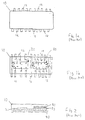
- FIG. la Shown in Figure la is a representation of a twenty pin Dual In-Line Package (DIP). Shown is an integrated circuit (IC) package 10, having twenty pins labeled 12, ten pins on each side of the IC package 10.
- Figure 1b shows the IC package 10 without a top cover, giving a view of how the pins 12 are connected within the IC package.
- the IC package 10 contains a chip 20 that has several bonding pads 14. Each bonding pad 14 is connected to one of the pins 12 of the IC package 10 in a conventional manner, such as by thermosonic or ultrasonic bonding.
- the chip 20 is coupled to eight of the twenty pins 12 of the IC package 10.
- the other twelve pins 12 of the IC package 10 are coupled to the bonding pads 14 of a chip 30.
- the chips 20 and 30 are attached to a common slug 40, shown in Figure 2.
- the common slug 40 is made from a metal material such as copper, but any suitable material can be used.
- the chips 20 and 30 can be directly soldered to, or otherwise physically attached to the slug, such as by eutectic bonding.
- the common slug 40 provides a stable base for handling during the creation of the IC package 10. Additionally, the slug acts as a large heat dissipater, removing heat from the chips 20 and 30 developed during their operation.
- an electrical insulating layer 50 ( Figure 2) is provided between the chip 30 and the common slug 40.
- This electrical insulating layer can an adhesive tape, for example, or a layer of molding compound.
- this electrical insulating layer 50 degrades the efficient heat transfer between the chip 30 and the common slug 40. Therefore, the chip 30, when electrically insulated from the common slug 40 by the electrical insulating layer 50, runs at a higher temperature than if it were directly soldered to the common slug 40. This higher temperature can degrade the performance of the chip 30, or even cause it to malfunction. However, in instances where the electrical insulating layer 50 is necessary, the chip cannot be soldered directly to the common slug 40 otherwise the electrical interference between the chip 20 and chip 30 would be present.
- One embodiment of the invention presents a multichip integrated circuit package having at least two chips electrically isolated from one another.
- a slug that is directly coupled to at least two chips, without any intervening insulating layers.
- the slug is physically separated at an appropriate place between the two chips, so that electrical interference between the two chips is eliminated.
- Another embodiment of the invention presents a method for creating a multichip integrated circuit package having at least two chips electrically isolated from one another.
- the method begins with directly attaching the two chips to a heat dissipating slug, preferably by soldering the chips to the slug.
- the heat dissipating slug has a pre-cut groove running between the chips. Once the chips are attached to the slug, the slug is molded into the multichip integrated circuit package. Then, the slug is physically separated into two pieces from the underside, the separation running along the pre-cut groove. In one embodiment, the slug is cut with a saw.
- Figure 1a is a top view of a twenty pin DIP according to the Prior Art.
- Figure 1b is a top view of the twenty pin DIP of Figure 1a, showing the connections of the pins, also according to the Prior Art.
- Figure 2 is a cross-sectional view of the twenty pin DIP of Figure 1a.
- Figure 3 is a cross-sectional diagram of a slug according to an embodiment of the invention.
- Figure 4 is a cross-sectional diagram of the slug of Figure 3, after further processing.
- FIG. 3 shows a slug 140 used in an embodiment of the invention.
- the slug 140 is made from copper and is roughly the same size of the IC package that will be ultimately produced.
- a groove 144 runs from one side of the slug 140 to the other side, effectively creating two die pads 146 and 148 in the slug. Because the slug 140 is still one large piece, it can be moved as a unit and provides a solid base for easy process handling. By including the groove 144 in the slug 140, two die pads 146 and 148 are delineated to indicate where semiconductor chips will be mounted.
- both chips 20 and 30 are power integrated circuits that generate large amounts of heat that is dissipated by the slug 140.
- the chips 20 and 30 can be attached to the slug 140 in any conventional means.
- the chips 20 and 30 are soldered directly to the slug 140, allowing the slug 140 to sink as much heat as possible from the chips 20 and 30 during operation.
- Another attachment method yielding good heat transfer from the chips 20, 30 to the slug 140 is eutectic bonding.
- a molded cavity 150 is formed around the slug in a conventional manner.
- the molded cavity 150 is made from any suitable material, such as ceramic, metal, epoxy resins, or insulating polymide.
- the die pads 146 and 148 of the slug are physically separated, such as by being sawed along the groove 144, producing a saw cut 154 ( Figure 4).
- the saw cut 154 is most easily made from the bottom of the molded cavity 150, which is opposite the direction of the groove 144 itself. While the saw cut 154 must be made in the general area of the groove 144, sawing the slug 140 is not an alignment-critical step, so long as the slug is ultimately separated between the chips 20 and 30. Other methods to physically separate the slug 140 along the groove are acceptable and fall within the scope of the invention.
- Cutting the slug 140 along the groove 144 separates the electrical connection that previously existed between the chip 20 and the chip 30, thus preventing electrical signals generated by one of the chips from interfering with the other.
- the groove 144 was filled with the material used to make the molded cavity 150 when the molded cavity was made.
- the saw cut 154 can also be filled with the same material after the saw cut is made, or it can be filled with another insulating material. The saw cut 154 can even be left as open space within the molded cavity 150. Once the saw cut 154 has been made, the slug 140 is separated into two pieces and the two resultant pieces are electrically separated from one another by the dielectric materials in the groove 144 and the saw cut 154.
- Figure 4 shows that the result of this embodiment of the invention includes both chips 20 and 30 soldered directly to the slug 140, thus maximizing the heat sinking capacity of the slug. Because neither of the chips 20 nor 30 has an intermediary layer of tape, adhesive, or molding compound between it and the slug 140, the heat transfer from the chips to the slug is as high as possible. Additionally, using the same process to bind the chips 20 and 30 to the slug 140 prevents the addition of extra materials and steps into the production process. For instance, using molding compound to attach the chip 30 while the chip 20 is soldered to the slug 140 causes several additional steps that are unnecessary if both chips are soldered to the slug. Also, using a single slug 140 allows the manufacturer to use simple leadframe structures rather than the complicated leadframes associated with a multipad slug design. Using simple leadframes makes the handling process easier for the manufacturer.
- the saw cut 154 combined with the groove 144 completely electrically insulates the chips 20 and 30 from one another, yet the direct connection of the chips to the slug 140 maintains the highest rate of heat transfer.
- the lost heat sink capacity of the slug 140 due to forming the trench 144 and the saw cut 154 is negligible.
- the IC package 10 shown in Figure 4 is a DIP package, nothing limits this process to only DIP packages. This process can be used for DIP packages, flat-packs, Pin Grid Arrays, quad packs, and the like. Also, the embodiment shown in Figure 4 only shows one saw cut 154 made in the slug 140, but as many saw cuts 154 as are necessary to electrically separate any number of chips mounted one the slug is specifically contemplated.
Landscapes
- Cooling Or The Like Of Semiconductors Or Solid State Devices (AREA)
- Lead Frames For Integrated Circuits (AREA)
Abstract
Description
Claims (22)
- An integrated electronic package containing a first and a second semiconductor circuit chip, the integrated electronic package comprising:a first slug coupled to the first semiconductor circuit chip in a first diepad area;a second slug coupled to the second semiconductor circuit chip in a second diepad area; anda dielectric material separating the first slug and the second slug.
- The integrated electronic package of claim 1 wherein the first slug and the second slug are formed from a single large slug.
- The integrated electronic package of claim 2 wherein the single large slug is made of copper.
- The integrated electronic package of claim 1 further comprising:
a molded cavity surrounding the first and second slugs. - The integrated electronic package of claim 4 wherein the molded cavity comprises the dielectric material separating the first slug and the second slug.
- The integrated circuit of claim 1 wherein the dielectric material fills a saw cut between the first slug and the second slug.
- The integrated circuit of claim 1 wherein the first semiconductor circuit chip is a power semiconductor.
- The integrated circuit of claim 1 wherein the first semiconductor circuit chip is soldered to the first slug.
- The integrated circuit of claim 1 further comprising:a third slug coupled to a third semiconductor circuit chip in a third diepad area; andthe dielectric material separating the second slug and the third slug.
- A method of making an integrated semiconductor package comprising:mounting a first semiconductor chip to a first die portion of a slug;mounting a second semiconductor chip to a second die portion of the slug;forming the slug in the integrated semiconductor package; andseparating the first die portion of the slug from the second die portion of the slug.
- The method of claim 10 wherein separating the first die portion of the slug from the second die portion of the slug comprises cutting through the slug with a saw.
- The method of claim 11 wherein the slug includes a groove lying between the first die portion and the second die portion, and wherein cutting through the slug with a saw comprises cutting the slug where the groove lies.
- The method of claim 11 wherein the slug includes a groove lying between the first die portion and the second die portion, and wherein cutting through the slug with a saw comprises cutting the slug from a side opposite a side of the slug that contains the groove until the groove is reached.
- The method of claim 11, further comprising:
after cutting through the slug with a saw, filling a cut left by the saw with a dielectric material. - The method of claim 10 wherein mounting a first semiconductor chip to a first die portion of a slug comprises soldering the first semiconductor chip to the first die portion.
- The method of claim 10 wherein mounting a first semiconductor chip to a first die portion of a slug comprises mounting a power semiconductor chip to the first die portion of the slug.
- The method of claim 10 wherein mounting a first semiconductor chip to a first die portion of a slug comprises mounting the first semiconductor chip to the first die portion of a copper slug.
- The method of claim 10 wherein forming the slug in the integrated semiconductor package comprises molding the integrated package around the plug.
- The method of claim 10 wherein separating the first die portion of the slug from the second die portion of the slug occurs after forming the slug in the integrated semiconductor package.
- An integrated power device containing a first power semiconductor chip and a second semiconductor chip, the integrated power device comprising:a package having a first slug and a second slug;the first power semiconductor chip bonded to the first slug in a diepad area of the first slug;the second semiconductor chip bonded to the second slug in a diepad area of the second slug; anda dielectric material separating the first slug from the second slug.
- The integrated power device of claim 18 wherein the package is a molded cavity comprising the dielectric material.
- The integrated power device of claim 18 wherein the first power semiconductor chip is soldered to the first slug.
Applications Claiming Priority (2)
| Application Number | Priority Date | Filing Date | Title |
|---|---|---|---|
| US09/507,558 US6473310B1 (en) | 2000-02-18 | 2000-02-18 | Insulated power multichip package |
| US507558 | 2000-02-18 |
Publications (3)
| Publication Number | Publication Date |
|---|---|
| EP1139421A2 true EP1139421A2 (en) | 2001-10-04 |
| EP1139421A3 EP1139421A3 (en) | 2003-03-12 |
| EP1139421B1 EP1139421B1 (en) | 2012-12-05 |
Family
ID=24019118
Family Applications (1)
| Application Number | Title | Priority Date | Filing Date |
|---|---|---|---|
| EP00123110A Expired - Lifetime EP1139421B1 (en) | 2000-02-18 | 2000-10-25 | Method of making an insulated power multichip package |
Country Status (2)
| Country | Link |
|---|---|
| US (1) | US6473310B1 (en) |
| EP (1) | EP1139421B1 (en) |
Families Citing this family (2)
| Publication number | Priority date | Publication date | Assignee | Title |
|---|---|---|---|---|
| US9524942B2 (en) * | 2013-12-18 | 2016-12-20 | Taiwan Semiconductor Manufacturing Company, Ltd. | Chip-on-substrate packaging on carrier |
| JP2022137337A (en) | 2021-03-09 | 2022-09-22 | キオクシア株式会社 | Semiconductor device |
Family Cites Families (10)
| Publication number | Priority date | Publication date | Assignee | Title |
|---|---|---|---|---|
| JPS5553433A (en) * | 1978-10-16 | 1980-04-18 | Hitachi Ltd | Manufacture of semiconductor device |
| US4561011A (en) * | 1982-10-05 | 1985-12-24 | Mitsubishi Denki Kabushiki Kaisha | Dimensionally stable semiconductor device |
| US5317194A (en) * | 1989-10-17 | 1994-05-31 | Kabushiki Kaisha Toshiba | Resin-sealed semiconductor device having intermediate silicon thermal dissipation means and embedded heat sink |
| JPH0548000A (en) * | 1991-08-13 | 1993-02-26 | Fujitsu Ltd | Semiconductor device |
| JP2911265B2 (en) * | 1991-09-27 | 1999-06-23 | 三洋電機株式会社 | Surface mount type semiconductor device |
| JPH0758254A (en) * | 1993-08-19 | 1995-03-03 | Fujitsu Ltd | Multi-chip module and manufacturing method thereof |
| JP3314574B2 (en) * | 1995-03-15 | 2002-08-12 | セイコーエプソン株式会社 | Method for manufacturing semiconductor device |
| KR100203934B1 (en) * | 1996-02-17 | 1999-06-15 | 윤종용 | Multi chip package using lead flame with patterning |
| JP3957803B2 (en) * | 1996-02-22 | 2007-08-15 | キヤノン株式会社 | Photoelectric conversion device |
| US6046501A (en) * | 1996-10-02 | 2000-04-04 | Matsushita Electric Industrial Co., Ltd. | RF-driven semiconductor device |
-
2000
- 2000-02-18 US US09/507,558 patent/US6473310B1/en not_active Expired - Lifetime
- 2000-10-25 EP EP00123110A patent/EP1139421B1/en not_active Expired - Lifetime
Also Published As
| Publication number | Publication date |
|---|---|
| US6473310B1 (en) | 2002-10-29 |
| EP1139421B1 (en) | 2012-12-05 |
| EP1139421A3 (en) | 2003-03-12 |
Similar Documents
| Publication | Publication Date | Title |
|---|---|---|
| US6043109A (en) | Method of fabricating wafer-level package | |
| US6545347B2 (en) | Enhanced leadless chip carrier | |
| US6818980B1 (en) | Stacked semiconductor package and method of manufacturing the same | |
| US6700187B2 (en) | Semiconductor package and method for manufacturing the same | |
| US20030011054A1 (en) | Power module package having improved heat dissipating capability | |
| KR100209760B1 (en) | Semiconductor package and its manufacturing method | |
| US20050051877A1 (en) | Semiconductor package having high quantity of I/O connections and method for fabricating the same | |
| CN100541748C (en) | Lead frame, semiconductor chip package, and method for manufacturing the package | |
| US7312525B2 (en) | Thermally enhanced package for an integrated circuit | |
| US8994161B2 (en) | Semiconductor device package and methods for producing same | |
| KR19980067735A (en) | Manufacturing method of semiconductor package | |
| US20080185698A1 (en) | Semiconductor package structure and carrier structure | |
| US6473310B1 (en) | Insulated power multichip package | |
| JP2651427B2 (en) | Method for manufacturing semiconductor device | |
| KR100206880B1 (en) | Columnar package with heat sink | |
| US6281096B1 (en) | Chip scale packaging process | |
| US6284570B1 (en) | Method of manufacturing a semiconductor component from a conductive substrate containing a plurality of vias | |
| JPS6318860B2 (en) | ||
| US12512393B2 (en) | Leadframe | |
| US20020053450A1 (en) | Wafer-level package | |
| KR19990086280A (en) | Semiconductor package | |
| KR20030050470A (en) | Semiconductor package and lead frame used in manufacturing such | |
| KR100379092B1 (en) | semiconductor package and its manufacturing method | |
| KR0161870B1 (en) | Structure and Manufacturing Method of Semiconductor Package | |
| JPH046105B2 (en) |
Legal Events
| Date | Code | Title | Description |
|---|---|---|---|
| PUAI | Public reference made under article 153(3) epc to a published international application that has entered the european phase |
Free format text: ORIGINAL CODE: 0009012 |
|
| AK | Designated contracting states |
Kind code of ref document: A2 Designated state(s): AT BE CH CY DE DK ES FI FR GB GR IE IT LI LU MC NL PT SE |
|
| AX | Request for extension of the european patent |
Free format text: AL;LT;LV;MK;RO;SI |
|
| PUAL | Search report despatched |
Free format text: ORIGINAL CODE: 0009013 |
|
| AK | Designated contracting states |
Kind code of ref document: A3 Designated state(s): AT BE CH CY DE DK ES FI FR GB GR IE IT LI LU MC NL PT SE |
|
| AX | Request for extension of the european patent |
Extension state: AL LT LV MK RO SI |
|
| RIC1 | Information provided on ipc code assigned before grant |
Ipc: 7H 01L 21/56 B Ipc: 7H 01L 23/433 A |
|
| 17P | Request for examination filed |
Effective date: 20030901 |
|
| AKX | Designation fees paid |
Designated state(s): DE FR GB IT |
|
| 17Q | First examination report despatched |
Effective date: 20061110 |
|
| RAP1 | Party data changed (applicant data changed or rights of an application transferred) |
Owner name: STMICROELECTRONICS SRL |
|
| GRAP | Despatch of communication of intention to grant a patent |
Free format text: ORIGINAL CODE: EPIDOSNIGR1 |
|
| RTI1 | Title (correction) |
Free format text: METHOD OF MAKING AN INSULATED POWER MULTICHIP PACKAGE |
|
| RAP1 | Party data changed (applicant data changed or rights of an application transferred) |
Owner name: STMICROELECTRONICS SRL |
|
| GRAS | Grant fee paid |
Free format text: ORIGINAL CODE: EPIDOSNIGR3 |
|
| GRAA | (expected) grant |
Free format text: ORIGINAL CODE: 0009210 |
|
| AK | Designated contracting states |
Kind code of ref document: B1 Designated state(s): DE FR GB IT |
|
| REG | Reference to a national code |
Ref country code: GB Ref legal event code: FG4D |
|
| REG | Reference to a national code |
Ref country code: DE Ref legal event code: R096 Ref document number: 60047673 Country of ref document: DE Effective date: 20130131 |
|
| PLBE | No opposition filed within time limit |
Free format text: ORIGINAL CODE: 0009261 |
|
| STAA | Information on the status of an ep patent application or granted ep patent |
Free format text: STATUS: NO OPPOSITION FILED WITHIN TIME LIMIT |
|
| 26N | No opposition filed |
Effective date: 20130906 |
|
| REG | Reference to a national code |
Ref country code: DE Ref legal event code: R097 Ref document number: 60047673 Country of ref document: DE Effective date: 20130906 |
|
| REG | Reference to a national code |
Ref country code: FR Ref legal event code: PLFP Year of fee payment: 16 |
|
| REG | Reference to a national code |
Ref country code: FR Ref legal event code: PLFP Year of fee payment: 17 |
|
| REG | Reference to a national code |
Ref country code: FR Ref legal event code: PLFP Year of fee payment: 18 |
|
| REG | Reference to a national code |
Ref country code: FR Ref legal event code: PLFP Year of fee payment: 19 |
|
| PGFP | Annual fee paid to national office [announced via postgrant information from national office to epo] |
Ref country code: FR Payment date: 20190919 Year of fee payment: 20 Ref country code: IT Payment date: 20190918 Year of fee payment: 20 |
|
| PGFP | Annual fee paid to national office [announced via postgrant information from national office to epo] |
Ref country code: GB Payment date: 20190923 Year of fee payment: 20 |
|
| PGFP | Annual fee paid to national office [announced via postgrant information from national office to epo] |
Ref country code: DE Payment date: 20190918 Year of fee payment: 20 |
|
| REG | Reference to a national code |
Ref country code: DE Ref legal event code: R071 Ref document number: 60047673 Country of ref document: DE |
|
| REG | Reference to a national code |
Ref country code: GB Ref legal event code: PE20 Expiry date: 20201024 |
|
| PG25 | Lapsed in a contracting state [announced via postgrant information from national office to epo] |
Ref country code: GB Free format text: LAPSE BECAUSE OF EXPIRATION OF PROTECTION Effective date: 20201024 |