EP1137070A2 - Fast line dump structure for solid state image sensor - Google Patents
Fast line dump structure for solid state image sensor Download PDFInfo
- Publication number
- EP1137070A2 EP1137070A2 EP01200923A EP01200923A EP1137070A2 EP 1137070 A2 EP1137070 A2 EP 1137070A2 EP 01200923 A EP01200923 A EP 01200923A EP 01200923 A EP01200923 A EP 01200923A EP 1137070 A2 EP1137070 A2 EP 1137070A2
- Authority
- EP
- European Patent Office
- Prior art keywords
- fast
- dump
- coupled device
- charge coupled
- dump gate
- Prior art date
- Legal status (The legal status is an assumption and is not a legal conclusion. Google has not performed a legal analysis and makes no representation as to the accuracy of the status listed.)
- Granted
Links
Images


Classifications
-
- H—ELECTRICITY
- H10—SEMICONDUCTOR DEVICES; ELECTRIC SOLID-STATE DEVICES NOT OTHERWISE PROVIDED FOR
- H10D—INORGANIC ELECTRIC SEMICONDUCTOR DEVICES
- H10D44/00—Charge transfer devices
- H10D44/40—Charge-coupled devices [CCD]
- H10D44/45—Charge-coupled devices [CCD] having field effect produced by insulated gate electrodes
- H10D44/454—Output structures
-
- H—ELECTRICITY
- H10—SEMICONDUCTOR DEVICES; ELECTRIC SOLID-STATE DEVICES NOT OTHERWISE PROVIDED FOR
- H10F—INORGANIC SEMICONDUCTOR DEVICES SENSITIVE TO INFRARED RADIATION, LIGHT, ELECTROMAGNETIC RADIATION OF SHORTER WAVELENGTH OR CORPUSCULAR RADIATION
- H10F39/00—Integrated devices, or assemblies of multiple devices, comprising at least one element covered by group H10F30/00, e.g. radiation detectors comprising photodiode arrays
- H10F39/10—Integrated devices
- H10F39/12—Image sensors
- H10F39/15—Charge-coupled device [CCD] image sensors
- H10F39/158—Charge-coupled device [CCD] image sensors having arrangements for blooming suppression
-
- H—ELECTRICITY
- H10—SEMICONDUCTOR DEVICES; ELECTRIC SOLID-STATE DEVICES NOT OTHERWISE PROVIDED FOR
- H10F—INORGANIC SEMICONDUCTOR DEVICES SENSITIVE TO INFRARED RADIATION, LIGHT, ELECTROMAGNETIC RADIATION OF SHORTER WAVELENGTH OR CORPUSCULAR RADIATION
- H10F39/00—Integrated devices, or assemblies of multiple devices, comprising at least one element covered by group H10F30/00, e.g. radiation detectors comprising photodiode arrays
- H10F39/80—Constructional details of image sensors
Definitions
- This invention relates to charge coupled devices, and more particularly to fast-dump gate formed within charge coupled devices.
- CCD charge coupled device
- FIG. 1 A conventional prior art device employing fast-dump gate structure is shown in Fig. 1 with two levels of polysilicon used to form the CCD electrodes.
- the two levels of polysilicon are indicated as H1 for the first level of polysilicon and H2 for the second level of polysilicon.
- Boron implants are used to form the two-phase CCD barrier regions in Fig. 1 and are indicated as BR1A for H1 and BR2A for H2.
- Each of the H1, H2 electrodes has an n-type buried channel beneath the poly1, poly2 electrodes in the prior art device shown in Fig. 1.
- CCD cell of the horizontal shift register which is to be connected to the fast-dump gate (shown as H1) has an effective width W2 that increases as the H1 cell of the horizontal shift register approaches the FDG along the length L2, yielding a well.
- Other prior art devices have an effective width W2 that decreases as it approaches the FDG along the length L2 creating a barrier.
- Fig. 2a is a cross sectional view of Fig. 1 along the line AA with associated potential diagrams 2b and 2c for cases where the effective channel width decreases as it approaches the fast-dump gate and the effective channel width increases as it approaches the fast-dump gate.
- W 2 eff W 1 eff
- a well is formed which is illustrated in Fig. 2c
- W 2 eff ⁇ W 1 eff a barrier is formed which is illustrated in Fig. 2b.
- the length L2 is a requirement that is dictated and determined by two level polysilicon space design rules to prevent H2 and FDG from shorting together.
- W 2 eff ⁇ W 1 eff a barrier exists which inhibits charge flow into FDD during fast-dump operation as shown in Fig. 2b.
- W 2 eff > W 1 eff no barrier exists in " L 2 " region and fast-dump operation works fine, but when FDG is off, a potential well exists in this region which can trap charge during HCCD readout as shown in Fig. 2c.
- Fig. 2d is a diagram illustrating the narrow width effect that is cured by the present invention. As the width increases, the potential shown as ⁇ (v) increases and then eventually flattens out.
- Fig. 3 is a cross sectional view of Fig. 1 along the line BB parallel to and through HCCD showing width W 1.
- the two levels of polysilicon are indicated as poly1 and poly2 for H1 and H2, respectively.
- the boron implants that form the barrier regions are indicated as BR1A for H1 and BR2A for H2.
- Each of the H1, H2 electrodes has an n-type buried channel beneath the poly1 poly2 electrodes.
- Fig. 4 is a cross-sectional view of Fig. 1 through the line CC and parallel to HCCD through the bottom part of H 1 showing second width, W 2.
- the boron implants resulting in p+ channel stops are illustrated as the identifying feature for W2.
- the p+ channel stops and Local Oxidized Silicon (LOCOS) provide channel isolation.
- Fig. 4 taken in conjunction with Fig. 1, illustrates that the width W2 increases to compensate for the narrowing effect of the boron implants used to create channel stops, resulting in the barriers and wells as previously discussed.
- the present invention solves many of the aforementioned problems within the prior art by providing a structure that comprises a fast-dump gate (FDG) and a fast-dump drain (FDD) that is connected to a horizontal readout register of a solid-state image sensor.
- FDG fast-dump gate
- FDD fast-dump drain
- lines of the captured image in the form of charge in the readout register
- This feature can be used, for example, to subsample the image or to read a frame out more quickly by throwing away selected lines.
- This structure uses a third layer of polysilicon (or other suitable gate material) to form the fast-dump gate which is in addition to the other two layers of gate material used to form the gates in the horizontal readout register. This allows the channel region under the FDG to form without the use of highly doped channel stop regions thereby eliminating the narrow-channel effect and any potential wells or barriers that may result in transfer inefficiency often times found with other structures.
- the present invention provides a solution to the problems within the prior art by providing a charge coupled device having a fast-dump gate (FDG) and a fast-dump drain (FDD) comprising: a charge coupled device having a first and a second level of polysilicon layers used to form electrodes on the charge coupled device; a third level polysilicon layer used to formed the fast-dump gate adjacent to at least one of the cells of the charge coupled device; and a drain that forms the fast-dump drain being operatively connected to the fast-dump gate.
- FDG fast-dump gate
- FDD fast-dump drain
- the invention advantages of not creating potential wells and barriers within fast-dump gate structures.
- FIG. 5 which illustrates a fast-dump structure on a charge-coupled device (CCD) as envisioned by the present invention wherein the fast-dump gate (FDG) is fabricated by use of a third level polysilicon.
- the present invention employs a third level of polysilicon which allows the FDG to be placed directly against the electrodes into the horizontal shift register area where the width is still W1, thereby, not incurring the potential barriers or wells that occur with increasing width W2 within the length L2 that are found in the prior art devices such as those shown in Fig. 1. The reasons for this is that the length L2 has been eliminated
- the fast-dump gate is an area within a charge-coupled device for removing charge from the charge-coupled device to a drain area.
- the present invention envisions employing a series of first level and second level polysilicon electrodes H1, H2 used within a horizontal charge-coupled device (HCCD) to form a two-phase device in a manner as shown in the prior art device of Fig. 1.
- the present invention envisions that the fast-dump gate be connected to the selected cells within the HCCD via implementation of a third level polysilicon such that the third level polysilicon can overlap the first and second levels of polysilicon electrodes H1, H2 without shorting them together.
- a drain is formed on the opposite side of the fast-dump gate that functions as the output node for charges that are to be dumped from the HCCD via the fast-dump gate connection.
- Fig. 1 Prior art, fast-dump gates are typically used in the area of a horizontal CCD shift register to: (1) read out selected data from the horizontal CCD in a windowing function; or (2) selectively dump lines of data from the horizontal shift register in sub-sampling modes.
- Prior art devices employ structures as shown in Fig. 1 with two levels of polysilicon to create the electrodes within the horizontal CCD.
- Fig. 2a is a cross sectional view of Fig. 1 along the line AA with associated potential diagrams for cases where the effective channel width decreases as it approaches the fast-dump gate and the effective channel width increases as it approaches the fast-dump gate.
- Fig. 4 is a cross-sectional view of Fig. 1 through the line CC and parallel to HCCD through bottom part of H1 showing second width, W2.
- the boron implants resulting in p+ channel stops are illustrated as the identifying features for W2.
- the p+ channel stops and the LOCOS confine charge to the channel region of width W2 existing between them.
- the drawn width W2 increases to compensate for the narrowing effect of the boron implants used to create channel stops possibly resulting in the potential barriers and wells as previously discussed.
- a third level polysilicon (Poly3) used in fabricating the fast-dump gate (FDG) eliminates the problem of matching effective channel widths to minimize wells or barriers at exit end of the H1 cell of the horizontal charge-coupled device. It should be noted that there is no structure that is equivalent to the L2/W2 region of Fig. 1. This is an important element within the context of the present invention.
- the effective channel length of the third level of polysilicon FDG gate is typically on the order of a couple of microns. Its effective width is virtually infinite since it typically extends along the entire length of the HCCD.
- the FDG could also be formed from a different polysilicon layer as long as there are three polysilicon layers.
- the FDG layer could be made from poly1 and the electrodes for H1 and H2 created by using poly2 and poly3 layers.
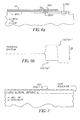
- FIG. 6a is a cross-section of Fig. 5 through line AA parallel to HCCD through the fast-dump gate (FDG) with an accompanying potential diagram as shown in Fig. 6b.
- the cross section shown in Fig. 6a appears similar to that shown in prior art device of Fig. 2a. Looking at the potential diagram in Fig. 6b, however, compared to those of Fig. 2b and Fig. 2c, it is readily apparent that the barriers of Fig. 2b and wells of Fig. 2c do not exist in the potential diagram seen in Fig. 6b for the present invention.
- Fig. 7 is not equivalent to the L2-W2 region of the prior art. It is equivalent to the BR2A region under FDG as shown (from the top) in Fig. 1. This BR2A region under FDG of Fig. 1 is not shown in cross section by any of the drawings. There are no confining LOCOS/p+ channel stop regions in the present invention, as shown Fig. 7, since they are not necessary.
- Fig. 7 is a cross section of Fig. 5 taken along line BB.
- the FDG has a virtually infinite width.
- a BR2A, or similar implant is not a requirement in this region for the present invention, but may be desirable depending on the clock voltages used. That is, it was used to shift the channel potential to a more desirable level for a given clock voltage to insure that the FDG region is truly "off' relative to the potentials under the HCCD phases so that charge does not inadvertently transfer into the FDG during HCCD readout.
Landscapes
- Solid State Image Pick-Up Elements (AREA)
- Transforming Light Signals Into Electric Signals (AREA)
Abstract
Description
Claims (10)
- A charge coupled device having a fast-dump gate (FDG) and a fast-dump drain (FDD) comprising:a charge coupled device formed upon a substrate, the charge coupled device having at least a first level and a second level of polysilicon layers used to form a plurality of electrodes on the charge coupled device;another polysilicon level used to formed gate adjacent to at least one of the electrodes of the charge coupled device to form the fast-dump gate; andwherein the fast-dump drain is coupled to the fast-dump gate away from the at least one electrode.
- The invention of claim 1 wherein the another polysilicon level is separated from the electrode by an isolation material.
- The invention of claim 1 wherein the at least one electrode that is adjacent the another polysilicon level is formed with a consistent width as it approaches the another polysilicon level.
- The invention of claim 3 wherein the fast-dump gate forms an electrical interface between the at least one electrode and the fast-dump drain.
- The invention of claim 4 wherein the electrical interface is formed without an effective resistivity change in the at least one electrode.
- A method of forming a fast-dump gate (FDG) and a fast-dump drain (FDD) on a charge coupled device having comprising the steps of:forming a charge coupled device formed upon a substrate with at least a first level and a second level of polysilicon layers used to form a plurality of electrodes on the charge coupled device;creating another polysilicon level to form the fast-dump gate adjacent to at least one of the electrodes of the charge coupled device; andcoupling the fast-dump drain to the fast-dump gate.
- The method of claim 6 wherein the step of creating further comprises creating the other polysilicon level such that it is separated from the electrode by an isolation material.
- The method of claim 6 wherein the creating further comprises creating the at least one electrode with a consistent width as it approaches the another polysilicon level.
- The method of claim 8 wherein the step of creating further comprises creating the fast-dump gate with an electrical interface between the at least one electrode and the fast-dump drain.
- The method of claim 9 wherein the step of creating further comprises creating the electrical interface is formed without an effective resistivity change in the at least one electrode.
Applications Claiming Priority (2)
| Application Number | Priority Date | Filing Date | Title |
|---|---|---|---|
| US09/533,050 US6507056B1 (en) | 2000-03-22 | 2000-03-22 | Fast line dump structure for solid state image sensor |
| US533050 | 2000-03-22 |
Publications (3)
| Publication Number | Publication Date |
|---|---|
| EP1137070A2 true EP1137070A2 (en) | 2001-09-26 |
| EP1137070A3 EP1137070A3 (en) | 2005-06-15 |
| EP1137070B1 EP1137070B1 (en) | 2014-06-04 |
Family
ID=24124251
Family Applications (1)
| Application Number | Title | Priority Date | Filing Date |
|---|---|---|---|
| EP01200923.9A Expired - Lifetime EP1137070B1 (en) | 2000-03-22 | 2001-03-12 | Fast line dump structure for solid state image sensor |
Country Status (3)
| Country | Link |
|---|---|
| US (2) | US6507056B1 (en) |
| EP (1) | EP1137070B1 (en) |
| JP (1) | JP2001298178A (en) |
Cited By (2)
| Publication number | Priority date | Publication date | Assignee | Title |
|---|---|---|---|---|
| WO2010141091A1 (en) * | 2009-06-01 | 2010-12-09 | Eastman Kodak Company | Ccd image sensors having multiple overflow drains |
| WO2011053485A1 (en) * | 2009-10-30 | 2011-05-05 | Eastman Kodak Company | Horizontal shift registers with lateral overflow drains |
Families Citing this family (3)
| Publication number | Priority date | Publication date | Assignee | Title |
|---|---|---|---|---|
| JP2001238134A (en) * | 2000-02-23 | 2001-08-31 | Sony Corp | Solid-state imaging device, driving method thereof, and camera system |
| CN104037186B (en) * | 2014-06-25 | 2017-01-18 | 中国兵器工业集团第二一四研究所苏州研发中心 | Halo resisting structure of charge carrier multiplication register |
| CN108258005B (en) * | 2018-01-11 | 2021-11-16 | 中国电子科技集团公司第四十四研究所 | CCD with rapid signal release function |
Family Cites Families (15)
| Publication number | Priority date | Publication date | Assignee | Title |
|---|---|---|---|---|
| US4040076A (en) * | 1976-07-28 | 1977-08-02 | Rca Corporation | Charge transfer skimming and reset circuit |
| JPS5721878A (en) * | 1980-07-15 | 1982-02-04 | Nec Corp | Solid state image pickp device and driving method therefor |
| US4611140A (en) | 1985-08-26 | 1986-09-09 | The United States Of America As Represented By The Secretary Of The Navy | Saw-CTD parallel to serial imager |
| US5121214A (en) | 1990-06-29 | 1992-06-09 | The United States Of America As Represented By The United States Department Of Energy | Method for eliminating artifacts in CCD imagers |
| JP3120465B2 (en) * | 1991-04-15 | 2000-12-25 | ソニー株式会社 | Solid-state imaging device |
| AU1995092A (en) | 1991-05-10 | 1992-12-30 | Q-Dot. Inc. | High-speed peristaltic ccd imager with gaas fet output |
| US5355165A (en) | 1992-08-06 | 1994-10-11 | Princeton Scientific Instruments, Inc. | Very high frame rate CCD imager |
| US5343297A (en) | 1992-09-17 | 1994-08-30 | General Electric Company | Charge amplifier with precise, integer gain |
| JPH06205298A (en) * | 1992-11-06 | 1994-07-22 | Sharp Corp | Charge-coupled solid-state imaging device |
| DE69419064T2 (en) * | 1993-04-20 | 1999-12-16 | Sony Corp., Tokio/Tokyo | Method and device for a solid-state imaging device |
| US5440343A (en) | 1994-02-28 | 1995-08-08 | Eastman Kodak Company | Motion/still electronic image sensing apparatus |
| US5668597A (en) | 1994-12-30 | 1997-09-16 | Eastman Kodak Company | Electronic camera with rapid automatic focus of an image upon a progressive scan image sensor |
| US5514886A (en) * | 1995-01-18 | 1996-05-07 | Eastman Kodak Company | Image sensor with improved output region for superior charge transfer characteristics |
| DE69632172T2 (en) * | 1995-02-21 | 2005-04-21 | Dalsa Corp | LOAD-COUPLED IMAGE RECORDING |
| US5990953A (en) * | 1995-12-15 | 1999-11-23 | Nec Corporation | Solid state imaging device having overflow drain region provided in parallel to CCD shift register |
-
2000
- 2000-03-22 US US09/533,050 patent/US6507056B1/en not_active Expired - Lifetime
-
2001
- 2001-03-06 JP JP2001061267A patent/JP2001298178A/en active Pending
- 2001-03-12 EP EP01200923.9A patent/EP1137070B1/en not_active Expired - Lifetime
-
2002
- 2002-11-13 US US10/293,672 patent/US6649442B2/en not_active Expired - Lifetime
Cited By (4)
| Publication number | Priority date | Publication date | Assignee | Title |
|---|---|---|---|---|
| WO2010141091A1 (en) * | 2009-06-01 | 2010-12-09 | Eastman Kodak Company | Ccd image sensors having multiple overflow drains |
| US8605187B2 (en) | 2009-06-01 | 2013-12-10 | Truesense Imaging, Inc. | CCD image sensors having multiple lateral overflow drain regions for a horizontal shift register |
| WO2011053485A1 (en) * | 2009-10-30 | 2011-05-05 | Eastman Kodak Company | Horizontal shift registers with lateral overflow drains |
| US8294802B2 (en) | 2009-10-30 | 2012-10-23 | Truesense Imaging, Inc. | CCD image sensors having multiple lateral overflow drain regions for a horizontal shift register |
Also Published As
| Publication number | Publication date |
|---|---|
| EP1137070B1 (en) | 2014-06-04 |
| US6649442B2 (en) | 2003-11-18 |
| US20030067019A1 (en) | 2003-04-10 |
| JP2001298178A (en) | 2001-10-26 |
| US6507056B1 (en) | 2003-01-14 |
| EP1137070A3 (en) | 2005-06-15 |
Similar Documents
| Publication | Publication Date | Title |
|---|---|---|
| US5029321A (en) | Solid state image sensing device formed of charge coupled devices | |
| US5656835A (en) | Solid state imager and its driving method | |
| CN100407434C (en) | Solid State Image Sensor | |
| EP0491922A1 (en) | Antiblooming structure for solid-state image sensor | |
| KR100266417B1 (en) | Amplfying type solid state imaging device and amplfying type solid state imaging apparatus | |
| US5402459A (en) | Frame transfer image sensor with electronic shutter | |
| US6693671B1 (en) | Fast-dump structure for full-frame image sensors with lod antiblooming structures | |
| CN101506968A (en) | Shielding floating gate tunneling element structure | |
| JPS62237761A (en) | charge coupled device | |
| EP1137070B1 (en) | Fast line dump structure for solid state image sensor | |
| EP1289020B1 (en) | A lateral overflow drain, antiblooming structure for CCD devices having improved breakdown voltage | |
| JPH07273315A (en) | CHARGE DETECTION DEVICE, MANUFACTURING METHOD THEREOF, AND CHARGE TRANSFER DETECTION DEVICE | |
| US5585298A (en) | Self aligned antiblooming structure for solid state image sensors | |
| US5256891A (en) | CCD electrode structure for image sensors | |
| JP2845216B2 (en) | Solid-state imaging device and method of manufacturing the same | |
| US6760073B1 (en) | Solid-state image sensor | |
| JPH0642540B2 (en) | Charge transfer device with anti-blooming barrier | |
| JPH07161970A (en) | Solid-state imaging device | |
| US5491354A (en) | Floating gate charge detection node | |
| US5313081A (en) | Solid-state imaging device with transport channels between photosensitive elements | |
| US6891243B2 (en) | Solid-state image pick-up device | |
| JP2877047B2 (en) | Solid-state imaging device | |
| US6417531B1 (en) | Charge transfer device with final potential well close to floating diffusion region | |
| JP2936153B2 (en) | Method for manufacturing solid-state imaging device | |
| JPH0319349A (en) | Charge-coupled device |
Legal Events
| Date | Code | Title | Description |
|---|---|---|---|
| PUAI | Public reference made under article 153(3) epc to a published international application that has entered the european phase |
Free format text: ORIGINAL CODE: 0009012 |
|
| AK | Designated contracting states |
Kind code of ref document: A2 Designated state(s): AT BE CH CY DE DK ES FI FR GB GR IE IT LI LU MC NL PT SE TR |
|
| AX | Request for extension of the european patent |
Free format text: AL;LT;LV;MK;RO;SI |
|
| PUAL | Search report despatched |
Free format text: ORIGINAL CODE: 0009013 |
|
| AK | Designated contracting states |
Kind code of ref document: A3 Designated state(s): AT BE CH CY DE DK ES FI FR GB GR IE IT LI LU MC NL PT SE TR |
|
| AX | Request for extension of the european patent |
Extension state: AL LT LV MK RO SI |
|
| RIC1 | Information provided on ipc code assigned before grant |
Ipc: 7H 01L 27/148 A Ipc: 7H 01L 29/768 B |
|
| 17P | Request for examination filed |
Effective date: 20051213 |
|
| AKX | Designation fees paid |
Designated state(s): DE FR GB NL |
|
| 17Q | First examination report despatched |
Effective date: 20060125 |
|
| 17Q | First examination report despatched |
Effective date: 20060125 |
|
| RAP1 | Party data changed (applicant data changed or rights of an application transferred) |
Owner name: TRUESENCE IMAGING, INC. |
|
| RAP1 | Party data changed (applicant data changed or rights of an application transferred) |
Owner name: TRUESENSE IMAGING, INC. |
|
| GRAP | Despatch of communication of intention to grant a patent |
Free format text: ORIGINAL CODE: EPIDOSNIGR1 |
|
| INTG | Intention to grant announced |
Effective date: 20140102 |
|
| GRAS | Grant fee paid |
Free format text: ORIGINAL CODE: EPIDOSNIGR3 |
|
| GRAA | (expected) grant |
Free format text: ORIGINAL CODE: 0009210 |
|
| AK | Designated contracting states |
Kind code of ref document: B1 Designated state(s): DE FR GB NL |
|
| REG | Reference to a national code |
Ref country code: GB Ref legal event code: FG4D |
|
| REG | Reference to a national code |
Ref country code: DE Ref legal event code: R096 Ref document number: 60148826 Country of ref document: DE Effective date: 20140710 |
|
| REG | Reference to a national code |
Ref country code: GB Ref legal event code: 732E Free format text: REGISTERED BETWEEN 20140904 AND 20140910 |
|
| REG | Reference to a national code |
Ref country code: NL Ref legal event code: VDEP Effective date: 20140604 |
|
| REG | Reference to a national code |
Ref country code: DE Ref legal event code: R082 Ref document number: 60148826 Country of ref document: DE Representative=s name: MEYER & PARTNER GBR, DE |
|
| REG | Reference to a national code |
Ref country code: DE Ref legal event code: R081 Ref document number: 60148826 Country of ref document: DE Owner name: SEMICONDUCTOR COMPONENTS INDUSTRIES, LLC (N. D, US Free format text: FORMER OWNER: TRUESENSE IMAGING, INC., NEWCASTLE, DEL., US Effective date: 20141121 Ref country code: DE Ref legal event code: R082 Ref document number: 60148826 Country of ref document: DE Representative=s name: MEYER & PARTNER GBR, DE Effective date: 20141121 Ref country code: DE Ref legal event code: R081 Ref document number: 60148826 Country of ref document: DE Owner name: SEMICONDUCTOR COMPONENTS INDUSTRIES, LLC (N. D, US Free format text: FORMER OWNER: EASTMAN KODAK CO., ROCHESTER, N.Y., US Effective date: 20140604 |
|
| PG25 | Lapsed in a contracting state [announced via postgrant information from national office to epo] |
Ref country code: NL Free format text: LAPSE BECAUSE OF FAILURE TO SUBMIT A TRANSLATION OF THE DESCRIPTION OR TO PAY THE FEE WITHIN THE PRESCRIBED TIME-LIMIT Effective date: 20140604 |
|
| REG | Reference to a national code |
Ref country code: DE Ref legal event code: R097 Ref document number: 60148826 Country of ref document: DE |
|
| PLBE | No opposition filed within time limit |
Free format text: ORIGINAL CODE: 0009261 |
|
| STAA | Information on the status of an ep patent application or granted ep patent |
Free format text: STATUS: NO OPPOSITION FILED WITHIN TIME LIMIT |
|
| 26N | No opposition filed |
Effective date: 20150305 |
|
| REG | Reference to a national code |
Ref country code: DE Ref legal event code: R097 Ref document number: 60148826 Country of ref document: DE Effective date: 20150305 |
|
| GBPC | Gb: european patent ceased through non-payment of renewal fee |
Effective date: 20150312 |
|
| REG | Reference to a national code |
Ref country code: FR Ref legal event code: ST Effective date: 20151130 |
|
| PG25 | Lapsed in a contracting state [announced via postgrant information from national office to epo] |
Ref country code: GB Free format text: LAPSE BECAUSE OF NON-PAYMENT OF DUE FEES Effective date: 20150312 |
|
| PG25 | Lapsed in a contracting state [announced via postgrant information from national office to epo] |
Ref country code: FR Free format text: LAPSE BECAUSE OF NON-PAYMENT OF DUE FEES Effective date: 20150331 |
|
| PGFP | Annual fee paid to national office [announced via postgrant information from national office to epo] |
Ref country code: DE Payment date: 20170331 Year of fee payment: 17 |
|
| REG | Reference to a national code |
Ref country code: DE Ref legal event code: R119 Ref document number: 60148826 Country of ref document: DE |
|
| PG25 | Lapsed in a contracting state [announced via postgrant information from national office to epo] |
Ref country code: DE Free format text: LAPSE BECAUSE OF NON-PAYMENT OF DUE FEES Effective date: 20181002 |