EP1136975A1 - Display device and method of controlling its brightness - Google Patents
Display device and method of controlling its brightness Download PDFInfo
- Publication number
- EP1136975A1 EP1136975A1 EP00957107A EP00957107A EP1136975A1 EP 1136975 A1 EP1136975 A1 EP 1136975A1 EP 00957107 A EP00957107 A EP 00957107A EP 00957107 A EP00957107 A EP 00957107A EP 1136975 A1 EP1136975 A1 EP 1136975A1
- Authority
- EP
- European Patent Office
- Prior art keywords
- display
- temperature
- luminance
- estimated value
- temperature difference
- Prior art date
- Legal status (The legal status is an assumption and is not a legal conclusion. Google has not performed a legal analysis and makes no representation as to the accuracy of the status listed.)
- Ceased
Links
Images





Classifications
-
- G—PHYSICS
- G09—EDUCATION; CRYPTOGRAPHY; DISPLAY; ADVERTISING; SEALS
- G09G—ARRANGEMENTS OR CIRCUITS FOR CONTROL OF INDICATING DEVICES USING STATIC MEANS TO PRESENT VARIABLE INFORMATION
- G09G3/00—Control arrangements or circuits, of interest only in connection with visual indicators other than cathode-ray tubes
- G09G3/20—Control arrangements or circuits, of interest only in connection with visual indicators other than cathode-ray tubes for presentation of an assembly of a number of characters, e.g. a page, by composing the assembly by combination of individual elements arranged in a matrix no fixed position being assigned to or needed to be assigned to the individual characters or partial characters
- G09G3/22—Control arrangements or circuits, of interest only in connection with visual indicators other than cathode-ray tubes for presentation of an assembly of a number of characters, e.g. a page, by composing the assembly by combination of individual elements arranged in a matrix no fixed position being assigned to or needed to be assigned to the individual characters or partial characters using controlled light sources
- G09G3/28—Control arrangements or circuits, of interest only in connection with visual indicators other than cathode-ray tubes for presentation of an assembly of a number of characters, e.g. a page, by composing the assembly by combination of individual elements arranged in a matrix no fixed position being assigned to or needed to be assigned to the individual characters or partial characters using controlled light sources using luminous gas-discharge panels, e.g. plasma panels
- G09G3/288—Control arrangements or circuits, of interest only in connection with visual indicators other than cathode-ray tubes for presentation of an assembly of a number of characters, e.g. a page, by composing the assembly by combination of individual elements arranged in a matrix no fixed position being assigned to or needed to be assigned to the individual characters or partial characters using controlled light sources using luminous gas-discharge panels, e.g. plasma panels using AC panels
- G09G3/296—Driving circuits for producing the waveforms applied to the driving electrodes
-
- G—PHYSICS
- G09—EDUCATION; CRYPTOGRAPHY; DISPLAY; ADVERTISING; SEALS
- G09G—ARRANGEMENTS OR CIRCUITS FOR CONTROL OF INDICATING DEVICES USING STATIC MEANS TO PRESENT VARIABLE INFORMATION
- G09G3/00—Control arrangements or circuits, of interest only in connection with visual indicators other than cathode-ray tubes
- G09G3/20—Control arrangements or circuits, of interest only in connection with visual indicators other than cathode-ray tubes for presentation of an assembly of a number of characters, e.g. a page, by composing the assembly by combination of individual elements arranged in a matrix no fixed position being assigned to or needed to be assigned to the individual characters or partial characters
- G09G3/22—Control arrangements or circuits, of interest only in connection with visual indicators other than cathode-ray tubes for presentation of an assembly of a number of characters, e.g. a page, by composing the assembly by combination of individual elements arranged in a matrix no fixed position being assigned to or needed to be assigned to the individual characters or partial characters using controlled light sources
- G09G3/28—Control arrangements or circuits, of interest only in connection with visual indicators other than cathode-ray tubes for presentation of an assembly of a number of characters, e.g. a page, by composing the assembly by combination of individual elements arranged in a matrix no fixed position being assigned to or needed to be assigned to the individual characters or partial characters using controlled light sources using luminous gas-discharge panels, e.g. plasma panels
- G09G3/288—Control arrangements or circuits, of interest only in connection with visual indicators other than cathode-ray tubes for presentation of an assembly of a number of characters, e.g. a page, by composing the assembly by combination of individual elements arranged in a matrix no fixed position being assigned to or needed to be assigned to the individual characters or partial characters using controlled light sources using luminous gas-discharge panels, e.g. plasma panels using AC panels
- G09G3/291—Control arrangements or circuits, of interest only in connection with visual indicators other than cathode-ray tubes for presentation of an assembly of a number of characters, e.g. a page, by composing the assembly by combination of individual elements arranged in a matrix no fixed position being assigned to or needed to be assigned to the individual characters or partial characters using controlled light sources using luminous gas-discharge panels, e.g. plasma panels using AC panels controlling the gas discharge to control a cell condition, e.g. by means of specific pulse shapes
- G09G3/294—Control arrangements or circuits, of interest only in connection with visual indicators other than cathode-ray tubes for presentation of an assembly of a number of characters, e.g. a page, by composing the assembly by combination of individual elements arranged in a matrix no fixed position being assigned to or needed to be assigned to the individual characters or partial characters using controlled light sources using luminous gas-discharge panels, e.g. plasma panels using AC panels controlling the gas discharge to control a cell condition, e.g. by means of specific pulse shapes for lighting or sustain discharge
- G09G3/2944—Control arrangements or circuits, of interest only in connection with visual indicators other than cathode-ray tubes for presentation of an assembly of a number of characters, e.g. a page, by composing the assembly by combination of individual elements arranged in a matrix no fixed position being assigned to or needed to be assigned to the individual characters or partial characters using controlled light sources using luminous gas-discharge panels, e.g. plasma panels using AC panels controlling the gas discharge to control a cell condition, e.g. by means of specific pulse shapes for lighting or sustain discharge by varying the frequency of sustain pulses or the number of sustain pulses proportionally in each subfield of the whole frame
-
- G—PHYSICS
- G09—EDUCATION; CRYPTOGRAPHY; DISPLAY; ADVERTISING; SEALS
- G09G—ARRANGEMENTS OR CIRCUITS FOR CONTROL OF INDICATING DEVICES USING STATIC MEANS TO PRESENT VARIABLE INFORMATION
- G09G2320/00—Control of display operating conditions
- G09G2320/02—Improving the quality of display appearance
- G09G2320/0271—Adjustment of the gradation levels within the range of the gradation scale, e.g. by redistribution or clipping
-
- G—PHYSICS
- G09—EDUCATION; CRYPTOGRAPHY; DISPLAY; ADVERTISING; SEALS
- G09G—ARRANGEMENTS OR CIRCUITS FOR CONTROL OF INDICATING DEVICES USING STATIC MEANS TO PRESENT VARIABLE INFORMATION
- G09G2320/00—Control of display operating conditions
- G09G2320/04—Maintaining the quality of display appearance
- G09G2320/041—Temperature compensation
-
- G—PHYSICS
- G09—EDUCATION; CRYPTOGRAPHY; DISPLAY; ADVERTISING; SEALS
- G09G—ARRANGEMENTS OR CIRCUITS FOR CONTROL OF INDICATING DEVICES USING STATIC MEANS TO PRESENT VARIABLE INFORMATION
- G09G2320/00—Control of display operating conditions
- G09G2320/06—Adjustment of display parameters
- G09G2320/0626—Adjustment of display parameters for control of overall brightness
-
- G—PHYSICS
- G09—EDUCATION; CRYPTOGRAPHY; DISPLAY; ADVERTISING; SEALS
- G09G—ARRANGEMENTS OR CIRCUITS FOR CONTROL OF INDICATING DEVICES USING STATIC MEANS TO PRESENT VARIABLE INFORMATION
- G09G2330/00—Aspects of power supply; Aspects of display protection and defect management
- G09G2330/04—Display protection
- G09G2330/045—Protection against panel overheating
Definitions
- the present invention relates to a display device for displaying an image with luminance corresponding to a video signal inputted from the exterior and a luminance control method therefor.
- Plasma display devices using PDPs have the advantage that thinning and larger screens are possible.
- images are displayed by utilizing light emission in cases where discharge cells composing pixels are discharged.
- heat is generated on a glass surface composing the PDP, so that the higher the luminance of an image becomes, the larger the amount of heat generation becomes. Therefore, the temperature of the glass surface is raised. In the worst case, the glass surface is damaged.
- an example of a conventional display device is a display device disclosed in JP-A-11-194745.
- the whole surface of a display screen is divided into a plurality of blocks, temperature estimated values are calculated with respect to all the blocks, and the maximum value of the calculated estimated temperatures is compared with a reference temperature to produce a luminance correction coefficient.
- the luminance of the display screen is controlled by the luminance correction coefficient.
- a display on which an image is displayed is generally fixed in its outer periphery. Damage to the display caused by the rise in the temperature with the increase in the luminance may occur in the vicinity of the outer periphery of the display in most cases. That is, the damage to the display depends on the temperature difference rather than the maximum temperature. Generally, the temperature difference between the outer periphery of the display where no heat is generated and the outer periphery of the display screen of the display where heat is generated is the largest. The display may be damaged by thermal stress created by the temperature difference in many cases.
- the luminance cannot be always controlled when excessive thermal stress is exerted on the outer periphery, which is most easily damaged, of the display, thereby making it impossible to reliably prevent the display from being damaged.
- the whole of the display screen is divided into a plurality of blocks, and the estimated temperatures are calculated with respect to all the blocks. Accordingly, operation processing becomes complicated, and long time is required to perform the operation processing. Particularly in recent years, it has been desired to make a display image highly precise.
- the number of pixels composing the display screen that is, the number of discharge cells has tended to be increased. In this case, the above-mentioned operation processing has increasingly become complicated, and the processing time is lengthened.
- An object of the present invention is to provide a display device capable of more reliably preventing a display from being damaged and a luminance control method therefor.
- Another object of the present invention is to provide a display device capable of more reliably preventing a display from being damaged in a small amount of operation and a luminance control method therefor.
- a display device comprises a display for displaying an image with luminance corresponding to a video signal inputted from the exterior; a temperature estimation circuit for estimating from the video signal a temperature estimated value corresponding to the temperature of a display screen of the display; an operation circuit for finding a temperature difference estimated value using a reference value corresponding to the temperature of the outer periphery of the display and the temperature estimated value; and a control circuit for controlling the luminance of the image displayed on the display on the basis of the temperature difference estimated value.
- the temperature estimated value corresponding to the temperature of the display screen of the display is estimated from the video signal, and the temperature difference estimated value is found using the temperature estimated value and the reference value corresponding to the temperature of the outer periphery of the display, to control the luminance of the image displayed on the display on the basis of the temperature difference estimated value.
- the display on which the image is displayed is fixed in its outer periphery. Accordingly, damage to the display caused by the rise in the temperature with the increase in the luminance may occur in the vicinity of the outer periphery of the display in most cases.
- the luminance is controlled depending on the temperature difference estimated value found from the temperature estimated value corresponding to the temperature of the display screen and the temperature of the outer periphery of the display, as described above, so that the luminance can be controlled on the basis of the temperature difference between the outer periphery of the display which most greatly affects the damage to the display and the display screen, thereby making it possible to more reliably prevent the display from being damaged.
- the temperature estimation circuit estimates the temperature estimated value corresponding to the temperature of the outer periphery of the display screen of the display.
- the temperature difference estimated value corresponding to the temperature of the outer periphery of the display screen of the display is estimated from the video signal, and the temperature difference estimated value is found using the temperature estimated value and the reference value corresponding to the temperature of the outer periphery of the display, to control the luminance of the image displayed on the display on the basis of the temperature difference estimated value.
- the temperature difference estimated value is found from the temperature estimated value corresponding to the temperature of the outer periphery of the display screen and the reference value corresponding to the temperature of the outer periphery of the display.
- the luminance can be controlled on the basis of the temperature difference between the outer periphery of the display which greatly affects the damage to the display and the outer periphery of the display screen closest to the outer periphery, thereby making it possible to more reliably prevent the display from being damaged.
- the temperature estimated value operated in order to find the temperature difference estimated value is limited to the temperature estimated value for the outer periphery of the display screen of the display. Accordingly, the amount of operation is made smaller than that in a case where the temperature estimated value on the whole of the display screen, so that the processing is simplified, and the processing time is shortened. As a result, it is possible to more reliably prevent the display from being damaged in a small amount of operation.
- the display comprises first and second boards between which a plurality of light emitting elements are formed and to which its outer periphery is fixed, and the outer periphery of the display includes a portion between the light emitting element positioned in the outermost periphery out of the plurality of light emitting elements and a fixed portion of the first and second boards.
- the reference value corresponds to the temperature of the portion between the light emitting element positioned in the outermost periphery and the fixing portion of the first and second boards. Accordingly, the luminance can be controlled using as a basis the temperature of the portion most easily damaged, thereby making it possible to more reliably prevent the display from being damaged.
- the temperature estimation circuit estimates the temperature estimated value by integrating data relating to the luminance from the video signal and subtracting the amount of dissipated heat therefrom, and the operation circuit subtracts the reference value from the temperature estimated value, to find the temperature difference estimated value.
- the data relating to the luminance is integrated from the video signal, and the amount of dissipated heat is subtracted therefrom, thereby making it possible to find the temperature estimated value corresponding to the truer temperature. Consequently, the luminance is controlled on the basis of the temperature difference estimated value obtained by subtracting the reference value from the temperature estimated value. Accordingly, it is possible to control the luminance with higher precision to more reliably prevent the display from being damaged.
- control circuit lowers the luminance of the image displayed on the display with the increase in the temperature difference estimated value.
- the luminance is lowered with the increase in the temperature difference estimated value, thereby making it possible to more reliably prevent the display from being damaged.
- control circuit lowers the maximum luminance of the image displayed on the display with the increase in the temperature difference estimated value.
- the maximum luminance is lowered with the increase in the temperature difference estimated value, thereby making it possible to more reliably prevent the display from being damaged as well as making it possible to display, when the luminance other than the maximum luminance is displayed as it is, a good image corresponding to the luminance of the video signal itself.
- the display displays the image with a gray scale corresponding to the video signal out of a plurality of gray scales, and the control circuit lowers the luminance of the image displayed on the display at the same ratio for each of the gray scales.
- the luminance is lowered at the same ratio for each gray scale, thereby making it possible to lower the luminance of the display without giving a visually uncomfortable feeling to a viewer.
- the display displays the image with a gray scale corresponding to the video signal using a plurality of light emitting formats which are the same in the total number of gray scales and differ in the number of light emitting pulses on each of the gray scales, and the control circuit controls the luminance of the image displayed on the display using the light emitting format selected depending on the temperature difference estimated value out of the plurality of light emitting formats.
- the luminance can be controlled by switching the plurality of light emitting formats in the order of their decreasing numbers of light emitting pulses on the same gray scale with the increase in the temperature difference estimated value, thereby making it possible to lower the luminance without greatly changing the total number of gray scales.
- control circuit divides the display screen of the display into a plurality of blocks, extracts from the plurality of blocks the peripheral block adjacent to the outer periphery of the display screen, and lowers the luminance of the peripheral block.
- the luminance of the peripheral block adjacent to the outer periphery of the display screen is lowered. Accordingly, the image in the block inside the display screen can be displayed with the luminance of the video signal itself, thereby making it possible to provide a display screen having no visually uncomfortable feeling by the viewer as well as to more reliably prevent the outer periphery of the display from being damaged.
- control circuit divides a display screen of the display into a plurality of blocks, extracts from the plurality of blocks the peripheral block adjacent to the outer periphery of the display screen, and makes the luminance of the peripheral block lower than that of the block inside the display screen of the display.
- the luminance of the peripheral block is made lower than that of the block inside the display screen. Accordingly, the luminance of the display screen is smoothly changed, thereby making it possible to provide a display screen having no visually uncomfortable feeling by the viewer as well as to more reliably prevent the outer periphery of the display from being damaged.
- the display device further comprises a block extraction circuit for dividing the display screen of the display into a plurality of blocks and extracting from the plurality of blocks the peripheral blocks adjacent to the outer periphery of the display screen, the temperature estimation circuit estimates the temperature estimated values for the peripheral blocks, the operation circuit finds a peripheral block temperature difference estimated value from the temperature estimated values estimated for the peripheral blocks, and the control circuit controls the luminance for each of the peripheral blocks on the basis of the peripheral block temperature difference estimated value.
- the display screen is divided into the plurality of blocks, and the luminance is controlled for each of the peripheral blocks adjacent to the outer periphery of the display screen. Accordingly, the luminance can be controlled more finely, thereby making it possible to provide a display screen having no visually uncomfortable feeling by the viewer as well as to more reliably prevent the outer periphery of the display from being damaged.
- control circuit controls the luminance for each of the peripheral blocks such that the amount of controlled luminance between the adjacent peripheral blocks is smoothly changed on the basis of the peripheral block temperature difference estimated value.
- the amount of controlled luminance between the adjacent peripheral blocks is smoothly changed. Accordingly, a display screen having no visually uncomfortable feeling can be provided for the viewer, and thermal stress created in the outer periphery of the display is smoothly changed, thereby making it possible to more reliably prevent the display from being damaged.
- the display device further comprises a block extraction circuit for dividing the display screen of the display into a plurality of blocks and extracting from the plurality of blocks the peripheral blocks adjacent to the outer periphery of the display screen, the temperature estimation circuit estimates the temperature estimated values for the peripheral blocks, the operation circuit finds, out of the temperature estimated values estimated for the peripheral blocks, peripheral block temperature difference estimated values for the peripheral blocks, and extracts from the peripheral block temperature difference estimated values the maximum peripheral block temperature difference estimated value, and the control circuit controls the luminance of the image displayed on the display on the basis of the maximum peripheral block temperature difference estimated value.
- the luminance is controlled using the maximum peripheral block temperature difference estimated value representing the largest temperature difference in the peripheral blocks, thereby making it possible to more reliably prevent the display from being damaged. Further, the luminance is controlled by the maximum peripheral block temperature difference estimated value, thereby simplifying processing for controlling the luminance.
- the reference value includes a plurality of reference values which differ depending on the position of the outer periphery of the display.
- the luminance of the image displayed on the display can be controlled using the plurality of reference values which differ depending on the position of the outer periphery of the display. Accordingly, a high reference value is set in a portion where the temperature is easily raised, while a low reference value is set in a portion where the temperature is not easily raised, thereby making it possible to control the luminance on the basis of each of the reference values. As a result, the display can be more reliably prevented from being damaged, and the luminance is not lowered any more than necessary.
- the display device further comprises a measurement circuit for measuring the temperature of the outer periphery of the display and outputting to the operation circuit the reference value corresponding to the measured temperature.
- the temperature of the outer periphery of the display is directly measured, thereby making it possible to control the luminance on the basis of the reference value corresponding to the temperature. Even when the reference value is changed by the variation in outside air temperature, for example, it is possible to reliably prevent the display from being damaged.
- a luminance control method for a display device is a luminance control method for a display device comprising a display for displaying an image with luminance corresponding to a video signal inputted from the exterior, characterized by comprising the steps of estimating from the video signal a temperature estimated value corresponding to the temperature of a display screen of the display; finding a temperature difference estimated value using a reference value corresponding to the temperature of the outer periphery of the display and the temperature estimated value; and controlling the luminance of the image displayed on the display on the basis of the temperature difference estimated value.
- the temperature estimated value corresponding to the temperature of the display screen of the display is estimated from the video signal, and the temperature difference estimated value is found using the temperature estimated value and the reference value corresponding to the temperature of the outer periphery of the display, to control the luminance of the image displayed on the display on the basis of the temperature difference estimated value.
- the display on which the image is displayed is fixed in its outer periphery. The damage to the display caused by the increase in the luminance may occur in the vicinity of the outer periphery of the display in most cases.
- the luminance is controlled depending on the temperature difference estimated value found from the temperature estimated value corresponding to the temperature of the display screen and the reference value corresponding to the temperature of the outer periphery of the display, thereby making it possible to control the luminance on the basis of the temperature difference between the outer periphery of the display which most greatly affects the damage to the display and the display screen and to more reliably prevent the display from being damaged.
- the temperature estimating step comprises the step of estimating the temperature estimated value corresponding to the temperature of the outer periphery of the display screen of the display.
- the temperature estimated value corresponding to the temperature of the outer periphery of the display screen of the display is estimated from the video signal, and the temperature difference estimated value is found using the temperature estimated value and the reference value corresponding to the temperature of the outer periphery of the display, to control the luminance of the image displayed on the display on the basis of the temperature difference estimated value.
- the temperature difference estimated value is found from the temperature estimated value corresponding to the temperature of the outer periphery of the display screen and the reference value corresponding to the temperature of the outer periphery of the display.
- the luminance can be controlled on the basis of the temperature difference between the outer periphery of the display which most greatly affects the damage to the display and the outer periphery of the display screen closest to the outer periphery of the display, thereby making it possible to more reliably prevent the display from being damaged.
- the temperature estimated value operated in order to find the temperature difference estimated value is limited to the temperature estimated value for the outer periphery of the display screen of the display. Accordingly, the amount of operation is made smaller than that in a case where the temperature estimated value on the whole of the display screen is operated, so that the processing is simplified, and the processing time is shortened. As a result, it is possible to more reliably prevent the display from being damaged in a small amount of operation.
- the display displays the image on a gray scale corresponding to the video signal using a plurality of light emitting formats which are the same in the total number of gray scales and differ in the number of light emitting pulses on each of the gray scales
- the controlling step comprises the step of controlling the luminance of the image displayed on the display using the light emitting format selected depending on the temperature difference estimated value out of the plurality of light emitting formats.
- the luminance can be controlled by switching the plurality of light emitting formats in the order of their decreasing numbers of light emitting pulses on the same gray scale with the increase in the temperature difference estimated value, thereby making it possible to lower the luminance without greatly changing the total number of gray scales.
- the controlling step comprises the step of dividing the display screen of the display into a plurality of blocks, extracting from the plurality of blocks the peripheral blocks adjacent to the outer periphery of the display screen, and lowering the luminance of the peripheral blocks.
- the luminance of the peripheral blocks adjacent to the outer periphery of the display screen is lowered. Accordingly, the image in the block inside the display screen can be displayed with the luminance of the video signal itself, thereby making it possible to provide a display screen having no visually uncomfortable feeling by the viewer as well as to more reliably prevent the outer periphery of the display from being damaged.
- the luminance control method for the display device further comprises the step of dividing the display screen of the display into a plurality of blocks and extracting from the plurality of blocks the peripheral blocks adjacent to the outer periphery of the display screen, the temperature estimating step comprises the step of estimating the temperature estimated values for the peripheral blocks, the temperature difference estimated value operating step comprises the step of finding a peripheral block temperature difference estimated value from the temperature estimated values estimated for the peripheral blocks, and the controlling step comprises the step of controlling the luminance for each of the peripheral blocks on the basis of the peripheral block temperature difference estimated value.
- the display screen is divided into the plurality of blocks, and the luminance is controlled for each of the peripheral blocks adjacent to the outer periphery of the display screen. Accordingly, the luminance can be controlled more finely, thereby making it possible to provide a display screen having no visually uncomfortable feeling by the viewer as well as to more reliably prevent the outer periphery of the display from being damaged.
- An AC-type plasma display device will be described as an example of a display device according to the present invention.
- a display device to which the present invention is applied is not particularly limited to the AC-type plasma display device.
- the present invention is similarly applicable to another display device, provided that the temperature of a display screen is changed by a change in luminance.
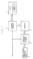
- FIG. 1 is a block diagram showing the configuration of the plasma display device according to the first embodiment of the present invention.
- the plasma display device shown in Fig. 1 comprises a display 1, a brightness controller 2, a controller 3, a temperature difference estimator 4, and a panel periphery temperature setter 5.
- a video signal VS is inputted to the brightness controller 2 and the temperature difference estimator 4.
- the panel periphery temperature setter 5 sets a reference value To representing the temperature of the panel outer periphery of the display 1, and outputs the reference value To to the temperature difference estimator 4.
- the temperature difference estimator 4 calculates a temperature difference estimated value Td representing the difference between the temperature of the panel outer periphery of the display 1 and the temperature of the display screen of the display 1 using the video signal VS and the reference value To, and outputs the temperature difference estimated value Td to the controller 3.
- the controller 3 outputs to the brightness controller 2 a brightness control signal LC for controlling the luminance of the display screen of the display 1 depending on the temperature difference estimated value Td.
- the brightness controller 2 outputs to the display 1 a data driver driving control signal DS, a scan driver driving control signal CS, and a sustain driver driving control signal US for displaying an image with luminance corresponding to the brightness control signal LC.
- Fig. 2 is a block diagram showing the configuration of the temperature difference estimator 4 shown in Fig. 1.
- the temperature difference estimator 4 comprises a periphery adjacent portion separator 41, an integration circuit 42, a dissipated heat subtraction circuit 43, and a subtracter 44.
- the periphery adjacent portion separator 41 receives the video signal VS, separates from the video signal VS a portion of a periphery adjacent portion adjacent to the outer periphery of the display screen of the display 1 from the video signal VS and outputs the separated portion to the integration circuit 42.
- the video signal VS includes not only an inherent video signal but also a vertical synchronizing signal, a horizontal synchronizing signal, and so forth.
- the periphery adjacent portion is separated using the horizontal synchronizing signal, the vertical synchronizing signal, and so forth.
- the integration circuit 42 integrates data relating to luminance from the video signal for the periphery adjacent portion separated by the periphery adjacent portion separator 41, for example, a luminance signal for the periphery adjacent portion, and outputs the integrated luminance signal to the dissipated heat subtraction circuit 43.
- the dissipated heat subtraction circuit 43 subtracts the amount of dissipated heat from the integrated luminance signal for the periphery adjacent portion to calculate a temperature estimated value Te representing the temperature of the periphery adjacent portion, and outputs the temperature estimated value Te to the subtracter 44.
- the subtracter 44 subtracts the reference value To for the panel outer periphery from the temperature estimated value Te for the periphery adjacent portion to find a temperature difference estimated value Td for the outer periphery of the display screen, and outputs the temperature difference estimated value Td to the controller 3.
- the controller 3 selects, out of a plurality of light emitting formats, the corresponding light emitting format depending on the temperature difference estimated value Td found by the processing, generates a brightness control signal LC including a light emitting pulse control signal EC for designating the selected light emitting format and a multiplication factor k in the selected light emitting format, and outputs the generated brightness control signal LC to the brightness controller 2.
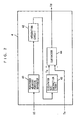
- Fig. 3 is a block diagram showing the configuration of the brightness controller 2 shown in Fig. 1.
- the brightness controller 2 comprises a multiplication circuit 21, a video signal/sub-field corresponder 22, and a sub-field pulse generator 23.
- the multiplication circuit 21 multiplies the video signal VS by the multiplication factor k included in the brightness control signal LC, and outputs to the video signal/sub-field corresponder 22 a video signal whose luminance has been controlled by the multiplication factor k.
- the video signal/sub-field corresponder 22 divides one field into a plurality of sub-fields to perform display. Accordingly, it generates from a video signal corresponding to one field image data for each sub-field in the light emitting format designated from the plurality of light emitting formats in response to the light emitting pulse control signal EC included in the brightness control signal LC, and outputs a data driver driving control signal DC corresponding to the image data for each sub-field to the display 1.
- the sub-field pulse generator 23 outputs to the display 1 the scan driver driving control signal CS and the sustain driver driving control signal US which correspond to each sub-field in the light emitting format designated from the plurality of light emitting formats in response to the light emitting pulse control signal EC included in the brightness control signal LC.
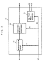
- Fig. 4 is a block diagram showing the configuration of the display 1 shown in Fig. 1.
- the display shown in Fig. 1 comprises a PDP (Plasma Display Panel) 11, a data driver 12, a scan driver 13, and a sustain driver 14.
- PDP Plasma Display Panel
- the data driver 12 is connected to a plurality of address electrodes (data electrodes) AD in the PDP 11.
- the scan driver 13 contains driving circuits respectively provided for scan electrodes SC in the PDP 11, and each of the driving circuits is connected to the corresponding scan electrode SC.
- the sustain driver 14 is together connected to a plurality of sustain electrodes SU in the PDP 11.
- the data driver 12 applies a write pulse to the corresponding address electrode AD in the PDP 11 during a write time period in accordance with the data driver driving control signal DS.
- the scan driver 13 successively applies the write pulses to the plurality of scan electrodes SC in the PDP 11 while shifting a shift pulse in the vertical scanning direction during the write time period in accordance with the scan driver driving control signal CS. Consequently, address discharges are induced in the corresponding discharge cell, and the discharge cell corresponding to the video signal VS is selected.
- the scan driver 13 applies periodical sustain pulses to the plurality of scan electrodes SC in the PDP 11 during a sustain time period in accordance with the scan driver driving control signal CS.
- the sustain driver 14 simultaneously applies sustain pulses which are shifted in phase by 180° from the sustain pulses applied to the scan electrodes SC in the sustain time period in accordance with the sustain driver driving control signal US. Consequently, sustain discharges are induced in the discharge cell selected in an address time period, and an image is displayed on the display screen with luminance corresponding to the video signal VS.
- Fig. 5 is a schematic view showing the configuration of the PDP 11 shown in Fig. 4.
- the PDP 11 comprises a plurality of address electrodes AD, a plurality of scan electrodes SC, a plurality of sustain electrodes SU, a surface glass board FP, a reverse glass board BP, and a barrier wall WA.
- the plurality of address electrodes AD are arranged in the vertical direction on the screen, and the plurality of scan electrodes SC and the plurality of sustain electrodes SU are arranged in the horizontal direction on the screen. Further, the sustain electrodes SU are together connected.
- a discharge cell CE is formed at each of the intersections of the address electrodes AD, the scan electrodes SC, and the sustain electrodes SU. Each of the discharge cells CE composes a pixel on the screen.
- the scan electrodes SC and the sustain electrodes SU are formed in the horizontal direction on the screen such that they are paired on the surface glass board FP, and are covered with a transparent dielectric layer and a protective layer.
- the address electrodes AD are formed in the vertical direction on the screen on the reverse glass board BP opposite to the surface glass board FP, a transparent dielectric layer is formed thereon, and a fluorescent member is further applied thereon.
- the barrier wall WA is provided between the address electrodes AD, so that the adjacent discharge cells CE are separated from each other.
- the address electrodes AD are provided every R, G, and B, and the barrier wall WA is provided between the address electrodes AD.
- the surface glass board FP and the reverse glass board BP are fixed with their outer peripheries joined to each other by a sealing glass SG.
- a sealing glass SG When the temperatures of the surface glass board FP and the reverse glass board BP are raised by causing the display cells CE to emit light, cracks occur in the vicinity of the sealing glass SG for the surface glass board FP and the reverse glass board BP. Consequently, the PDP 11 may be damaged in many cases.
- the luminance of the PDP 11 is controlled on the basis of the temperature difference in the portion most easily damaged. Therefore, the temperature difference estimated value Td is found in the following manner.
- a portion, including at least the discharge cells CE positioned in the outermost periphery (for example, a square frame portion indicated by hatching), of the display screen of the PDP 11, that is, a portion where the discharge cells CE are formed is taken as a periphery adjacent portion NE, to separate a video signal in the region by the periphery adjacent portion separator 41 in the temperature difference estimator 4.
- the separated video signal is integrated, for example, by the integration circuit 42 and the dissipated heat subtraction circuit 43, to find a temperature estimated value Te representing the temperature of the periphery adjacent portion NE.
- the panel periphery temperature setter 5 takes a portion of the sealing glass SG for the surface glass board FP and the reverse glass board BP and a portion between the discharge cell CE positioned in the outermost periphery and the sealing glass SG as the panel outer periphery, and sets the temperature of the portion as a reference value To. Consequently, the reference value To for the panel outer periphery is subtracted from the temperature estimated value Te for the periphery adjacent portion NE, thereby operating the temperature difference estimated value Td for the outer periphery of the display screen. Consequently, the luminance is controlled, as described later, using the temperature difference estimated value Td representing the temperature difference in the portion most easily damaged, thereby more reliably preventing the PDP 11 form being damaged.
- the PDP 11 corresponds to a display
- the temperature difference estimator 4 corresponds to a temperature estimation circuit and an operation circuit
- the brightness controller 2, the controller 3, the data driver 12, the scan driver 13, and the sustain driver 14 correspond to a control circuit
- the periphery adjacent portion separator 41, the integration circuit 42, and the dissipated heat subtraction circuit 43 correspond to a temperature estimation circuit
- the subtracter 44 corresponds to an operation circuit.
- gray scale display method using five types of light emitting formats in which the total number of gray scales is 256, and one field is divided into eight sub-fields to perform display as an example of a gray scale display method for the display device configured as described above.
- the gray scale display method to which the present invention is applied is not particularly limited to the following example. Another gray scale display method may be used.
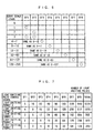
- Fig. 6 is a diagram showing sub-fields where sustain discharges should be induced when the display screen is displayed at each gray scale level in a case where the total number of gray scales is 256.
- the sub-fields SF1 to SF8 are successively respectively weighted with brightness values 1, 2, 4, 8, 16, 32, 64, and 128, for example.
- Each of the weights is a value proportional to the luminance of the display screen, for example, the number of times of light emission in each of the discharge cells.
- the sub-fields SF1 to SF8 used for causing the discharge cell to emit light at each gray scale level are indicated by ⁇ .
- the sub-field SF1 (a weight 1) may be used.
- the sub-field SF1 and the sub-field SF2 (a weight 2) may be used, and a corresponding column in each of the sub-fields is assigned ⁇ . If the sub-fields are combined with each other to cause the discharge cell to emit light in a number of times of light emission corresponding to the weight, gray scale display can be performed at each of the gray scale levels 0 to 255.
- the number of sub-fields obtained by the division, the weights, and so forth are not particularly limited to those in the above-mentioned example, and various modifications are possible.
- Fig. 7 is a diagram showing the number of light emitting pulses in each of the sub-fields SF1 to SF8 in each of the five types of light emitting formats A to E.
- Each of the light emitting formats A to E is determined by the controller 2 depending on the temperature estimated value Td, as described later, and is specified by the light emitting pulse control signal EC.
- the total number of light emitting pulses is 1275, five light emitting pulses are assigned to the sub-field SF1, 10 light emitting pulses are assigned to the sub-field SF2, and 20, 40, 80, 160, 320, and 640 light emitting pulses are similarly assigned, respectively, to the sub-fields SF3 to SF8.
- the total number of light emitting pulses is 1020 in the light emitting format B, the total number of light emitting pulses is 765 in the light emitting format C, the total number of light emitting pulses is 510 in the light emitting format D, and the total number of light emitting pulses in the light emitting format E is 255.
- the number of light emitting pulses, as shown, is assigned to each of the sub-fields SF1 to SF8.
- the light emitting formats A to E differ in the number of light emitting pulses and luminance even at the same gray scale level. That is, when the luminance in the light emitting format E is used as a basis (once), the luminance in the light emitting format D is twice that in the light emitting format E, the luminance in the light emitting format C is three times that in the light emitting format E, the luminance in the light emitting format B is four times that in the light emitting format E, and the luminance in the light emitting format A is five times that in the light emitting format E. Consequently, the light emitting formats are successively switched from A to E, therefore, the luminance of the display screen can be lowered without significantly changing the total number of gray scales.
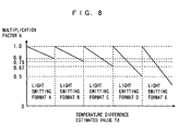
- Fig. 8 is a diagram showing the relationship between a temperature difference estimated value Td and a multiplication factor k in a case where the light emitting formats A to E are combined with each other to induce sustain discharges.
- the relationship between the temperature difference estimated value Td and the multiplication factor k shown in Fig. 8 is previously stored in the controller 3.
- the light emitting format and the multiplication factor k which correspond to the temperature difference estimated value Td estimated by the temperature difference estimator 4 are specified by the controller 3.
- the multiplication factor k linearly decreases from 1.0 to 0.8.
- the multiplication factor k decreases from 1.0 to 0.75.
- the multiplication factor k decreases from 1.0 to 0.67.
- the multiplication factor k decreases from 1.0 to 0.5.
- the multiplication factor k decreases from 1.0.
- the multiplication factor is returned to 1.0 when the light emitting format is switched after decreasing from 1.0. That is, the total number of light emitting pulses in the light emitting format A is 1275, and the total number of light emitting pulses in the light emitting format B is 1020. Accordingly, the ratio of the numbers of pulses is 0.8.
- the multiplication factor k is switched from 0.8 to 1.0, thereby making it possible to reduce the number of light emitting pulses at a predetermined ratio depending on the temperature difference estimated value Td before and after the switching and to linearly control the luminance of the display screen. The same is true even at the time of later switching the light emitting format.
- the multiplication factor k is thus switched depending on the total number of light emitting pulses at the time of switching the light emitting format, thereby making it possible to linearly control the luminance of the display screen depending on the temperature difference estimated value Td even when the image is displayed using the different light emitting format as well as to lower the luminance without extremely reducing the total number of gray scales.
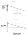
- the temperature difference estimated value Td increases, and the luminance after the control linearly decreases, as shown in Fig. 9, thereby making it possible to lower the luminance of the display screen depending on the temperature difference estimated value Td.
- the luminance in a case where the luminance is not decreased, that is, the temperature difference estimated value Td is zero is 5 (a relative value).
- the light emitting format is not particularly limited to the above-mentioned example.
- the sustain discharges may be induced using only the light emitting format A out of the light emitting formats A to E.
- Fig. 10 is a diagram showing the relationship between the temperature difference estimated value Td and the multiplication factor k in a case where the light emitting format A is used.
- the multiplication factor k is outputted as 1.0.
- the video signal VS is multiplexed by the multiplication factor k by the multiplication circuit 21, thereby making it possible to lower the luminance of the display screen depending on the temperature difference estimated value Td, as in a case shown in Fig. 9.
- a video signal for the periphery adjacent portion is separated from a video signal VS by the periphery adjacent portion separator 41, a luminance signal in the video signal for the periphery adjacent portion is integrated by the integration circuit 42, and the amount of dissipated heat is subtracted by the dissipated heat subtraction circuit 43, to calculate a temperature estimated value Te for the periphery adjacent portion.
- a reference value To for the panel outer periphery set by the panel periphery temperature setter 5 is subtracted from the temperature estimated value Te for the periphery adjacent portion by the subtracter 44, so that a temperature difference estimated value Td for the periphery of the display screen is calculated.
- a light emitting format and a multiplication factor k which correspond to the temperature difference estimated value Td are then determined by the controller 3, so that a light emitting pulse control signal EC corresponding to the determined light emitting format and a brightness control signal LC including the determined multiplication factor k are generated.
- the video signal VS is multiplied by the multiplication factor k included in the brightness control signal LC by the multiplication circuit 21, so that a video signal whose luminance has been controlled is generated depending on the multiplication factor k.
- Image data for each sub-field in the light emitting format corresponding to the light emitting pulse control signal EC included in the brightness control signal LC is then generated from the video signal corresponding to one field whose luminance has been controlled by the video signal/sub-field corresponder 22, and a data driver driving control signal DS corresponding to the image data is outputted.
- a scan driver driving control signal CS and a sustain driver driving control signal US which correspond to each sub-field in the light emitting format corresponding to the light emitting pulse control signal EC are generated by the sub-field pulse generator 23.
- address discharges in the corresponding discharge cell are induced in response to the data driver driving control signal DS and the scan driver driving control signal CS by the data driver 12 and the scan driver 13, and sustain discharges are then induced in the discharge cell in which the address discharges have been induced in response to the scan driver driving control signal CS and the sustain driver driving control signal US by the scan driver 13 and the sustain driver 14. Accordingly, an image is displayed on the display screen with the luminance controlled depending on the multiplication factor k. The larger the temperature difference estimated value Td becomes, the lower the luminance of the display screen becomes.
- the temperature estimated value Te corresponding to the temperature of the periphery adjacent portion of the display screen of the PDP 11 is estimated from the video signal VS, the temperature difference estimated value Td is found using the temperature estimated value Te and the reference value To corresponding to the temperature of the panel outer periphery, the light emitting format and the multiplication factor k which correspond to the temperature difference estimated value Td are determined, and the luminance of the display screen of the PDP 11 is controlled by the light emitting format and the multiplication factor k which have been determined.
- the luminance can be controlled on the basis of the temperature difference between the panel outer periphery which greatly affects the damage to the PDP 11 and the periphery adjacent portion closest to the panel outer periphery, thereby making it possible to more reliably prevent the PDP 11 from being damaged. Further, only the temperature estimated value Td for the periphery adjacent portion is operated, so that the amount of operation is reduced, thereby making it possible to simplify the processing as well as to shorten the processing time.
- the second luminance control method is a method of dividing the display screen into a plurality of blocks and controlling the luminance of the peripheral block adjacent to the outer periphery of the display screen out of the blocks obtained by the division.
- the control method is carried out by the controller 3 outputting a multiplication factor k corresponding to a temperature difference estimated value Td when a video signal VS corresponding to the peripheral block is inputted to the multiplication circuit 21, outputting one as the multiplication factor k when the video signal VS corresponding to the inner block other than the peripheral block is inputted to the multiplication circuit 21, and multiplying the video signal VS by the multiplication factors k by the multiplication circuit 21.
- a vertical synchronizing signal and a horizontal synchronizing signal are inputted to the controller 3 through the temperature difference estimator 4, and the display screen is divided using the horizontal synchronizing signal and the vertical synchronizing signal, for example, to specify the peripheral block.
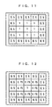
- Fig. 11 is a diagram showing an example of a multiplication factor k for each block in a case where the luminance of the peripheral block is controlled.
- the display screen is divided into a total of 25 blocks, that is, five blocks in the longitudinal direction and five blocks in the transverse direction.
- the number of divisions of the display screen is not particularly limited to that in this example. The number can be suitably determined depending on the number of pixels composing the display screen, and the processing capabilities of the temperature difference estimator 4, the controller 3, and so forth, for example.
- a discharge cell in the outermost periphery is positioned in the outermost periphery of each peripheral block, and an outer frame indicates the outer periphery of the PDP 11.
- the multiplication factor k for the peripheral blocks (blocks indicated by hatching) is set to 0.5, and the multiplication factor k for the other inner blocks is set to one.
- the multiplication factor k is decreased only in a portion of the peripheral block most easily damaged, and the luminance of this portion is reduced. Consequently, the PDP 11 can be more reliably prevented from being damaged without lowering the luminance of the inside of the display screen.
- the third luminance control method is a method of controlling the luminance of each of blocks such that the luminance of the peripheral block is made lower than that of the inner block.
- the control method is carried out by the controller 3 outputting a multiplication factor k corresponding to a temperature difference estimated value Td when a video signal VS corresponding to the peripheral block is inputted to the multiplication circuit 21, increasing the multiplication factor k depending on the position of each of the blocks such that the multiplication factor for the block at the center is one when the video signal VS corresponding to the inner block other than the peripheral block is inputted to the multiplication circuit 21, and multiplying the video signal VS by the multiplication factor k by the multiplication circuit 21.
- Fig. 12 is a diagram showing an example of the multiplication factor k for each block in a case where the luminance of the blocks is controlled such that the luminance of the peripheral blocks is made lower than that of the inner blocks.
- the multiplication factor k for the peripheral blocks is set to 0.5
- the multiplication factor k for the inner blocks is set to 0.75
- the multiplication factor k for the block at the center is set to one.
- the luminance of a portion of the peripheral block most easily damaged is most greatly reduced, thereby making it possible to more reliably prevent the PDP 11 from being damaged.
- the amount of change of the multiplication factor k depending on the position of the block is not particularly limited to that in the above-mentioned example. Various modifications are possible. For example, the amount of change on the side of the outer periphery is made larger.
- Fig. 13 is a block diagram showing the configuration of the plasma display device according to the second embodiment of the present invention.
- the plasma display device shown in Fig. 13 divides a display screen of a display 1 into a plurality of blocks, finds a peripheral block temperature difference estimated value Tbd for each peripheral block adjacent to the outer periphery of the display screen out of the blocks obtained by the division, and controls luminance using the peripheral block temperature difference estimated value Tbd. Consequently, the plasma display device shown in Fig. 13 is the same as the plasma display device shown in Fig. 1 except that the temperature difference estimator 4 is changed into a temperature difference estimator 4A for estimating the peripheral block temperature difference estimated value Tbd for each peripheral block. Accordingly, the same portions are assigned the same reference numerals and hence, the description thereof is not repeated. Only the temperature difference estimator 4A obtained by the change will be described in detail.
- Fig. 14 is a block diagram showing the configuration of the temperature difference estimator 4A shown in Fig. 13.
- the temperature difference estimator 4A shown in Fig. 14 is the same as the temperature difference estimator 4 shown in Fig. 2 except that a block separator 45 is added between a periphery adjacent portion separator 41 and an integration circuit 42. Accordingly, the same portions are assigned the same reference numerals and hence, the description thereof is not repeated.
- the block separator 45 is connected to the periphery adjacent portion separator 41, and receives a video signal for a periphery adjacent portion which is outputted from the periphery adjacent portion separator 41, separates the video signal for each peripheral block adjacent to the outer periphery of the display screen, and outputs the divided video signal to the integration circuit 42.
- a vertical synchronizing signal and a horizontal synchronizing signal, for example, included in the video signal VS are inputted to the block separator 45, so that the peripheral block is extracted using the horizontal synchronizing signal and the vertical synchronizing signal, for example.
- each processing is performed, as in the first embodiment, for each peripheral block.
- the peripheral block temperature difference estimated value Tbd is outputted for each peripheral block from a subtracter 44.
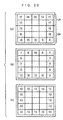
- Fig. 15 is a diagram showing an example of a temperature estimated value Tb and a peripheral block temperature difference estimated value Tbd which are estimated for each peripheral block.
- Tb temperature estimated value
- Tbd peripheral block temperature difference estimated value
- the number of divisions of the display screen is not particularly limited to that in this example. The number can be suitably determined depending on the number of pixels composing the display screen, and the processing capabilities of the temperature difference estimator 4A, the controller 3, and so forth, for example.
- a discharge cell in the outermost periphery is positioned in the outermost periphery of the peripheral block, and an outer frame indicates the outer periphery of a PDP 11.
- the temperature estimated value Tb is determined for each peripheral block.
- the temperature estimated value Tb for the peripheral block in the upper left of the display screen is 17
- the temperature estimated value Tb for the peripheral block adjacent thereto on the right side is 18, and the temperature estimated value Tb for the peripheral block adjacent thereto on the right side is 20.
- the temperature estimated value Tb is thus estimated for each peripheral block.
- a reference value To is subtracted from each of the temperature estimated values Tb shown in Fig. 15(a).
- the reference value To for the peripheral blocks included in two rows in an upper part UR is set to 10
- a multiplication factor k is determined, as in Fig. 8, for each of the peripheral blocks using the value, and the luminance of the peripheral block is controlled depending on the multiplication factor k.
- an address electrode AD is wired to its upper part, as shown in Fig. 5. Accordingly, a vent for cooling, for example, is provided in its lower part.
- the temperature of the upper part tends to be raised more easily, as compared with the temperature of the lower part. Consequently, a high reference value is set with respect to the upper part UR in the PDP 11, and a lower reference value is set in the lower part DR, as compared with that in the upper part UR, thereby making it possible to calculate a temperature difference estimated value closer to thermal stress actually created in the panel outer periphery of the PDP 11.
- the PDP 11 can be more reliably prevented from being damaged, and the luminance is not lowered any more than necessary.
- a method of controlling luminance using a plurality of reference values which differ depending on the position of the panel outer periphery of the PDP 11, as described above, is also applicable to other embodiments.
- the controller 3 uses the peripheral block temperature difference estimated value Tbd for each peripheral block found in the above-mentioned manner, to output a brightness control signal LC to a brightness controller 2 such that luminance is controlled for each peripheral block.
- the brightness controller 2 outputs to the display 1 an address driver driving control signal AD, a scan driver driving control signal CS, and a sustain driver driving control signal US for controlling the luminance for each peripheral block in response to a brightness control signal LC.
- the luminance is controlled for each peripheral block in response to each of the inputted driving control signals by each luminance control method described below.
- the present embodiment is the same as the first embodiment except that the temperature difference estimator 4A corresponds to a temperature estimation circuit and an operation circuit, and the block separator 45 corresponds to a block extraction circuit.
- the first luminance control method is a method of estimating a temperature estimated value Tb for each peripheral block, subtracting a reference value To from the temperature estimated value Tb for the peripheral block to find a peripheral block temperature difference estimated value Tbd, and controlling luminance depending on the peripheral block temperature difference estimated value Tbd for the peripheral block.
- a multiplication factor k corresponding to the peripheral block temperature difference estimated value Tbd for the peripheral block is outputted when a video signal VS corresponding to the peripheral block separated by the block separator 45 is inputted to a multiplication circuit 21, one is outputted as the multiplication factor k when the video signal VS corresponding to the inner block other than the peripheral block is inputted to the multiplication circuit 21, and the video signal VS is multiplied by the multiplication factors k by the multiplication circuit 21.
- Fig. 16 is a diagram showing an example of a peripheral block temperature difference estimated value Tbd and a multiplication factor for each peripheral block in a case where luminance is controlled for the peripheral block by the first luminance control method.
- a peripheral block temperature difference estimated value Tbd is estimated for each peripheral block. That is, it is assumed that the peripheral block temperature difference estimated value Tbd for the peripheral blocks positioned at the respective centers of the upper side, the lower side, the left side, and the right side of the display screen is 20, and the peripheral block temperature difference estimated value Tbd for the other peripheral blocks is zero.
- a multiplication factor k for the peripheral block is as shown in Fig. 16(b). That is, the multiplication factor k for the peripheral blocks at the respective centers of the upper side, the lower side, the left side, and the right side is 0.5, and the multiplication factor k for the other peripheral blocks is one. The luminance of each of the peripheral blocks is controlled depending on the multiplication factor k.
- the multiplication factor k is decreased only in the peripheral block where the peripheral block temperature difference estimated value Tbd is large, and only the luminance of this portion is reduced. Consequently, only the luminance of the peripheral block most easily damaged is lowered without lowering the luminance of the other block, thereby making it possible to more reliably prevent the PDP 11 from being damaged.
- the second luminance control method is for controlling luminance for each peripheral block on the basis of a peripheral block temperature difference estimated value Tbd' obtained by subjecting a peripheral block temperature difference value Tbd between adjacent peripheral blocks to filtering processing such that the amount of controlled luminance between the adjacent peripheral blocks is smoothly changed.
- the peripheral block temperature difference estimated value Tbd is subjected to filtering processing such as integration or interpolation between the adjacent peripheral blocks by the controller 3, a multiplication factor k corresponding to the peripheral block temperature difference estimated value Tbd' after the filtering processing is outputted, and a video signal VS corresponding to the peripheral block is multiplied by the multiplication factor k in the multiplication circuit 21.
- Fig. 17 is a diagram showing an example of a peripheral block temperature difference estimated value Tbd for each peripheral block, a peripheral block temperature difference estimated value Tbd' after filtering processing, and a multiplication factor k in a case where luminance is controlled for each peripheral block such that the amount of controlled luminance is smoothly changed by the second luminance control method.
- a peripheral block temperature difference estimated value Tbd is estimated for each peripheral block, as in Fig. 16(a).
- the peripheral block temperature difference estimated value Tbd is then filtered by interpolation between the adjacent peripheral blocks.
- the peripheral block temperature difference estimated value Tbd' after the filtering processing is as shown in Fig. 17(b).
- a peripheral block temperature difference estimated value Tbd for the peripheral block between the peripheral block having a peripheral block temperature difference estimated value Tbd of 20 and the peripheral block having a peripheral block temperature difference estimated value Tbd of 0 is interpolated from zero to 10.
- a multiplication factor k for each of the peripheral blocks is as shown in Fig. 17(c).
- the multiplication factor k for the peripheral blocks at the respective centers of the upper side, the lower side, the left side and the right side is 0.5
- the multiplication factor k for the peripheral block positioned at each vertex of the display screen is one
- the multiplication factor k for the intermediate peripheral block is 0.75.
- the multiplication factor k is smoothly changed.
- the luminance of each of the peripheral blocks is controlled depending on the multiplication factor k.
- the luminance of a portion of the peripheral block most easily damaged is most greatly reduced, and thermal stress in the peripheral block is smoothly changed, thereby making it possible to more reliably prevent the PDP 11 from being damaged.
- the multiplication factor k is gradually smoothly changed. Accordingly, the change in the luminance by the change in the multiplication factor k is difficult to visually know, thereby making it possible to prevent the image quality from being degraded.
- the change in the multiplication factor k by the filtering processing is not particularly limited. Various modifications are possible. For example, the multiplication factor k is exponentially changed.
- Fig. 18 is a block diagram showing the configuration of the plasma display device according to the third embodiment of the present invention.
- the plasma display device shown in Fig. 18 divides a display screen of a display 1 into a plurality of blocks, finds a peripheral block temperature difference estimated value Tbd for each peripheral block adjacent to the outer periphery of the display screen out of the blocks obtained by the division, extracts the maximum peripheral block temperature difference estimated value Tmax out of the peripheral block temperature difference estimated values Tbd, and controls luminance using the maximum peripheral block temperature difference estimated value Tmax. Consequently, the plasma display device shown in Fig. 18 is the same as the plasma display device shown in Fig. 13 except that the temperature difference estimator 4A is changed into a temperature difference estimator 4B for estimating the peripheral block temperature difference estimated value Tbd for each peripheral block and extracting the maximum peripheral block temperature difference estimated value Tmax. Accordingly, the same portions are assigned the same reference numerals and hence, the description thereof is not repeated. Only the temperature difference estimator 4B obtained by the change will be described in detail.
- Fig. 19 is a block diagram showing the configuration of the temperature difference estimator 4B shown in Fig. 18.
- the temperature difference estimator 4B shown in Fig. 18 is the same as the temperature difference estimator 4A shown in Fig. 14 except that a maximum selector 46 is added in a stage succeeding a subtracter 44. Accordingly, the same portions are assigned the same reference numerals and hence, the description thereof is not repeated.
- the maximum selector 46 is connected to the subtracter 44, and selects a maximum peripheral block temperature difference estimated value Tb out of the peripheral block temperature difference estimated values Tbd for the peripheral blocks in one field, that is, one display screen which are outputted from the subtracter 44 and extracts the maximum peripheral block temperature difference estimated value Tbd as a maximum peripheral block temperature difference estimated value Tmax.
- Fig. 20 is a diagram showing an example of a temperature estimated value Tb, a peripheral block temperature difference estimated value Tbd, and a maximum peripheral block temperature difference estimated value Tmax which are estimated for each peripheral block.
- a temperature estimated value Tb is estimated for each peripheral block, as in Fig. 15(a).
- a peripheral block temperature difference estimated value Tbd for each peripheral block is then found, as in Fig. 15(b).
- a peripheral block at the lower left corner having a maximum peripheral block temperature difference estimated value Tbd (13 in the example shown in Fig. 20) out of peripheral block temperature difference estimated values Tbd shown in Fig. 20(b) is selected, and 13 which is the peripheral block temperature difference estimated value Tbd for the peripheral block is taken as the maximum peripheral block temperature difference estimated value Tmax.
- the peripheral block temperature difference estimated values Tbd for all the peripheral blocks are replaced with the maximum peripheral block temperature difference estimated value Tmax.
- a multiplication factor k is determined, as in Fig. 8, for each peripheral block using the maximum peripheral block temperature difference estimated value Tmax, and the luminance of each of the peripheral blocks is controlled depending on the multiplication factor k.
- a controller 3 uses the maximum peripheral block temperature difference estimated value Tmax found in the above-mentioned manner, to output a brightness control signal LC to a brightness controller 2 such that the luminance is controlled for each peripheral block.
- the brightness controller 2 outputs to a display 1 an address driver driving control signal AD, a scan driver driving control signal CS, and a sustain driver driving control signal US for controlling luminance for each peripheral block depending on the brightness control signal LC.
- the luminance is controlled in response to each of the inputted driving control signals.
- the present embodiment is the same as the second embodiment except that a temperature difference estimator 4B corresponds to a temperature estimation circuit and an operation circuit.
- the luminance control method for each of the above-mentioned embodiments can be used, thereby making it possible to obtain the same effect.
- the luminance is controlled using the maximum peripheral block temperature difference estimated value Tmax representing the largest temperature difference in the peripheral blocks, thereby making it possible to more reliably prevent the PDP 11 from being damaged. Further, the luminance is controlled by one maximum peripheral block temperature difference estimated value, so that processing for controlling the luminance is simplified.
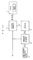
- Fig. 21 is a block diagram showing the configuration of the plasma display device according to the fourth embodiment of the present invention.
- the plasma display device shown in Fig. 21 is the same as the plasma display device shown in Fig. 1 except that a temperature measuring unit 6 is added. Accordingly, the same portions are assigned the same reference numerals and hence, the description thereof is not repeated.
- the temperature measuring unit 6 is connected to a panel periphery temperature setter 5, and directly measures the temperature of the panel outer periphery of a PDP 11 and outputs the measured temperature to the panel periphery temperature setter 5.
- the panel periphery temperature setter 5 sets a reference value To corresponding to the measured temperature and outputs the set reference value To to a temperature difference estimator 4. After that, the subsequent processing is performed, as in the first embodiment, so that luminance is controlled.
- the present embodiment is the same as the first embodiment except that the panel periphery temperature setter 5 and the temperature measuring unit 6 correspond to a measurement circuit.
- the luminance control method in the first embodiment can be similarly used, thereby making it possible to obtain the same effect.
- a luminance control method in another embodiment can be also similarly used, thereby making it possible to obtain the same effect.
- the temperature of the panel outer periphery is directly measured, and the luminance can be controlled on the basis of the reference value To corresponding to the temperature. Even when the reference value To is changed due to the variation in outer air temperature, for example, therefore, the PDP 11 can be more reliably prevented from being damaged.
- the number of measuring points in the temperature measuring unit 6 may be one or plural in the panel outer periphery. When a plurality of points are measured, a reference value may be set for each of the measuring points, or a reference value may be set, for example, with respect to the average of the results of the measurement of the plurality of points.
- the video signal VS is multiplexed by the multiplication factor k included in the brightness control signal LC outputted from the controller 3 in the multiplication circuit 21 to control the luminance
- the maximum luminance of an image displayed on the PDP 11 may be lowered by changing the multiplication circuit 21 into a limiting circuit for limiting the maximum luminance of the video signal, outputting an upper-limit value of the maximum luminance corresponding to the temperature difference estimated value from the controller 3, and limiting only luminance exceeding the upper-limit value of the maximum luminance by the limiting circuit.
Landscapes
- Engineering & Computer Science (AREA)
- Physics & Mathematics (AREA)
- Power Engineering (AREA)
- Plasma & Fusion (AREA)
- Computer Hardware Design (AREA)
- General Physics & Mathematics (AREA)
- Theoretical Computer Science (AREA)
- Control Of Gas Discharge Display Tubes (AREA)
- Control Of Indicators Other Than Cathode Ray Tubes (AREA)
- Transforming Electric Information Into Light Information (AREA)
- Control Of El Displays (AREA)
- Electroluminescent Light Sources (AREA)
Abstract
A temperature difference estimated value is found from
a video signal using a temperature estimated value
representing the temperature of the panel outer periphery of
a display screen of a PDP and a reference value representing
the temperature of the panel outer periphery of the PDP which
is outputted from a panel periphery temperature setter by a
temperature difference estimator, and the luminance of an
image displayed on a display is controlled depending on the
temperature difference estimated value by a controller and
a brightness controller.
Description
The present invention relates to a display device for
displaying an image with luminance corresponding to a video
signal inputted from the exterior and a luminance control
method therefor.
Plasma display devices using PDPs (Plasma Display
Panels) have the advantage that thinning and larger screens
are possible. In the plasma display devices, images are
displayed by utilizing light emission in cases where
discharge cells composing pixels are discharged. As light
is thus emitted, heat is generated on a glass surface
composing the PDP, so that the higher the luminance of an image
becomes, the larger the amount of heat generation becomes.
Therefore, the temperature of the glass surface is raised.
In the worst case, the glass surface is damaged.
In order to solve the above-mentioned problem, an
example of a conventional display device is a display device
disclosed in JP-A-11-194745. In the display device, the whole
surface of a display screen is divided into a plurality of
blocks, temperature estimated values are calculated with
respect to all the blocks, and the maximum value of the
calculated estimated temperatures is compared with a
reference temperature to produce a luminance correction
coefficient. The luminance of the display screen is
controlled by the luminance correction coefficient.
A display on which an image is displayed is generally
fixed in its outer periphery. Damage to the display caused
by the rise in the temperature with the increase in the
luminance may occur in the vicinity of the outer periphery
of the display in most cases. That is, the damage to the
display depends on the temperature difference rather than the
maximum temperature. Generally, the temperature difference
between the outer periphery of the display where no heat is
generated and the outer periphery of the display screen of
the display where heat is generated is the largest. The
display may be damaged by thermal stress created by the
temperature difference in many cases.
In the conventional display device, however, only when
the maximum value of the estimated temperatures reaches not
less than the reference temperature, that is, when the
temperature of any portion on the display screen exceeds its
certain upper-limit value, the luminance is controlled.
Therefore, the luminance cannot be always controlled when
excessive thermal stress is exerted on the outer periphery,
which is most easily damaged, of the display, thereby making
it impossible to reliably prevent the display from being
damaged.
In the conventional display device, the whole of the
display screen is divided into a plurality of blocks, and the
estimated temperatures are calculated with respect to all the
blocks. Accordingly, operation processing becomes
complicated, and long time is required to perform the
operation processing. Particularly in recent years, it has
been desired to make a display image highly precise. The
number of pixels composing the display screen, that is, the
number of discharge cells has tended to be increased. In this
case, the above-mentioned operation processing has
increasingly become complicated, and the processing time is
lengthened.
An object of the present invention is to provide a
display device capable of more reliably preventing a display
from being damaged and a luminance control method therefor.
Another object of the present invention is to provide
a display device capable of more reliably preventing a display
from being damaged in a small amount of operation and a
luminance control method therefor.
A display device according to an aspect of the present
invention comprises a display for displaying an image with
luminance corresponding to a video signal inputted from the
exterior; a temperature estimation circuit for estimating
from the video signal a temperature estimated value
corresponding to the temperature of a display screen of the
display; an operation circuit for finding a temperature
difference estimated value using a reference value
corresponding to the temperature of the outer periphery of
the display and the temperature estimated value; and a control
circuit for controlling the luminance of the image displayed
on the display on the basis of the temperature difference
estimated value.
In the display device, the temperature estimated value
corresponding to the temperature of the display screen of the
display is estimated from the video signal, and the
temperature difference estimated value is found using the
temperature estimated value and the reference value
corresponding to the temperature of the outer periphery of
the display, to control the luminance of the image displayed
on the display on the basis of the temperature difference
estimated value. Generally, the display on which the image
is displayed is fixed in its outer periphery. Accordingly,
damage to the display caused by the rise in the temperature
with the increase in the luminance may occur in the vicinity
of the outer periphery of the display in most cases.
Therefore, the luminance is controlled depending on the
temperature difference estimated value found from the
temperature estimated value corresponding to the temperature
of the display screen and the temperature of the outer
periphery of the display, as described above, so that the
luminance can be controlled on the basis of the temperature
difference between the outer periphery of the display which
most greatly affects the damage to the display and the display
screen, thereby making it possible to more reliably prevent
the display from being damaged.
It is preferable that the temperature estimation
circuit estimates the temperature estimated value
corresponding to the temperature of the outer periphery of
the display screen of the display.
In this case, the temperature difference estimated
value corresponding to the temperature of the outer periphery
of the display screen of the display is estimated from the
video signal, and the temperature difference estimated value
is found using the temperature estimated value and the
reference value corresponding to the temperature of the outer
periphery of the display, to control the luminance of the
image displayed on the display on the basis of the temperature
difference estimated value. The temperature difference
estimated value is found from the temperature estimated value
corresponding to the temperature of the outer periphery of
the display screen and the reference value corresponding to
the temperature of the outer periphery of the display.
Accordingly, the luminance can be controlled on the basis of
the temperature difference between the outer periphery of the
display which greatly affects the damage to the display and
the outer periphery of the display screen closest to the outer
periphery, thereby making it possible to more reliably
prevent the display from being damaged. Further, the
temperature estimated value operated in order to find the
temperature difference estimated value is limited to the
temperature estimated value for the outer periphery of the
display screen of the display. Accordingly, the amount of
operation is made smaller than that in a case where the
temperature estimated value on the whole of the display
screen, so that the processing is simplified, and the
processing time is shortened. As a result, it is possible
to more reliably prevent the display from being damaged in
a small amount of operation.
It is preferable that the display comprises first and
second boards between which a plurality of light emitting
elements are formed and to which its outer periphery is fixed,
and the outer periphery of the display includes a portion
between the light emitting element positioned in the
outermost periphery out of the plurality of light emitting
elements and a fixed portion of the first and second boards.
In this case, the reference value corresponds to the
temperature of the portion between the light emitting element
positioned in the outermost periphery and the fixing portion
of the first and second boards. Accordingly, the luminance
can be controlled using as a basis the temperature of the
portion most easily damaged, thereby making it possible to
more reliably prevent the display from being damaged.
It is preferable that the temperature estimation
circuit estimates the temperature estimated value by
integrating data relating to the luminance from the video
signal and subtracting the amount of dissipated heat
therefrom, and the operation circuit subtracts the reference
value from the temperature estimated value, to find the
temperature difference estimated value.
In this case, the data relating to the luminance is
integrated from the video signal, and the amount of dissipated
heat is subtracted therefrom, thereby making it possible to
find the temperature estimated value corresponding to the
truer temperature. Consequently, the luminance is controlled
on the basis of the temperature difference estimated value
obtained by subtracting the reference value from the
temperature estimated value. Accordingly, it is possible to
control the luminance with higher precision to more reliably
prevent the display from being damaged.
It is preferable that the control circuit lowers the
luminance of the image displayed on the display with the
increase in the temperature difference estimated value.
In this case, the luminance is lowered with the increase
in the temperature difference estimated value, thereby making
it possible to more reliably prevent the display from being
damaged.
It is preferable that the control circuit lowers the
maximum luminance of the image displayed on the display with
the increase in the temperature difference estimated value.
In this case, the maximum luminance is lowered with the
increase in the temperature difference estimated value,
thereby making it possible to more reliably prevent the
display from being damaged as well as making it possible to
display, when the luminance other than the maximum luminance
is displayed as it is, a good image corresponding to the
luminance of the video signal itself.
It is preferable that the display displays the image
with a gray scale corresponding to the video signal out of
a plurality of gray scales, and the control circuit lowers
the luminance of the image displayed on the display at the
same ratio for each of the gray scales.
In this case, the luminance is lowered at the same ratio
for each gray scale, thereby making it possible to lower the
luminance of the display without giving a visually
uncomfortable feeling to a viewer.
It is preferable that the display displays the image
with a gray scale corresponding to the video signal using a
plurality of light emitting formats which are the same in the
total number of gray scales and differ in the number of light
emitting pulses on each of the gray scales, and the control
circuit controls the luminance of the image displayed on the
display using the light emitting format selected depending
on the temperature difference estimated value out of the
plurality of light emitting formats.
In this case, the luminance can be controlled by
switching the plurality of light emitting formats in the order
of their decreasing numbers of light emitting pulses on the
same gray scale with the increase in the temperature
difference estimated value, thereby making it possible to
lower the luminance without greatly changing the total number
of gray scales.
It is preferable that the control circuit divides the
display screen of the display into a plurality of blocks,
extracts from the plurality of blocks the peripheral block
adjacent to the outer periphery of the display screen, and
lowers the luminance of the peripheral block.
In this case, the luminance of the peripheral block
adjacent to the outer periphery of the display screen is
lowered. Accordingly, the image in the block inside the
display screen can be displayed with the luminance of the
video signal itself, thereby making it possible to provide
a display screen having no visually uncomfortable feeling by
the viewer as well as to more reliably prevent the outer
periphery of the display from being damaged.
It is preferable that the control circuit divides a
display screen of the display into a plurality of blocks,
extracts from the plurality of blocks the peripheral block
adjacent to the outer periphery of the display screen, and
makes the luminance of the peripheral block lower than that
of the block inside the display screen of the display.
In this case, the luminance of the peripheral block is
made lower than that of the block inside the display screen.
Accordingly, the luminance of the display screen is smoothly
changed, thereby making it possible to provide a display
screen having no visually uncomfortable feeling by the viewer
as well as to more reliably prevent the outer periphery of
the display from being damaged.
It is preferable that the display device further
comprises a block extraction circuit for dividing the display
screen of the display into a plurality of blocks and
extracting from the plurality of blocks the peripheral blocks
adjacent to the outer periphery of the display screen, the
temperature estimation circuit estimates the temperature
estimated values for the peripheral blocks, the operation
circuit finds a peripheral block temperature difference
estimated value from the temperature estimated values
estimated for the peripheral blocks, and the control circuit
controls the luminance for each of the peripheral blocks on
the basis of the peripheral block temperature difference
estimated value.
In this case, the display screen is divided into the
plurality of blocks, and the luminance is controlled for each
of the peripheral blocks adjacent to the outer periphery of
the display screen. Accordingly, the luminance can be
controlled more finely, thereby making it possible to provide
a display screen having no visually uncomfortable feeling by
the viewer as well as to more reliably prevent the outer
periphery of the display from being damaged.
It is preferable that the control circuit controls the
luminance for each of the peripheral blocks such that the
amount of controlled luminance between the adjacent
peripheral blocks is smoothly changed on the basis of the
peripheral block temperature difference estimated value.
In this case, the amount of controlled luminance between
the adjacent peripheral blocks is smoothly changed.
Accordingly, a display screen having no visually
uncomfortable feeling can be provided for the viewer, and
thermal stress created in the outer periphery of the display
is smoothly changed, thereby making it possible to more
reliably prevent the display from being damaged.
It is preferable that the display device further
comprises a block extraction circuit for dividing the display
screen of the display into a plurality of blocks and
extracting from the plurality of blocks the peripheral blocks
adjacent to the outer periphery of the display screen, the
temperature estimation circuit estimates the temperature
estimated values for the peripheral blocks, the operation
circuit finds, out of the temperature estimated values
estimated for the peripheral blocks, peripheral block
temperature difference estimated values for the peripheral
blocks, and extracts from the peripheral block temperature
difference estimated values the maximum peripheral block
temperature difference estimated value, and the control
circuit controls the luminance of the image displayed on the
display on the basis of the maximum peripheral block
temperature difference estimated value.
In this case, the luminance is controlled using the
maximum peripheral block temperature difference estimated
value representing the largest temperature difference in the
peripheral blocks, thereby making it possible to more
reliably prevent the display from being damaged. Further,
the luminance is controlled by the maximum peripheral block
temperature difference estimated value, thereby simplifying
processing for controlling the luminance.
It is preferable that the reference value includes a
plurality of reference values which differ depending on the
position of the outer periphery of the display.
In this case, the luminance of the image displayed on
the display can be controlled using the plurality of reference
values which differ depending on the position of the outer
periphery of the display. Accordingly, a high reference value
is set in a portion where the temperature is easily raised,
while a low reference value is set in a portion where the
temperature is not easily raised, thereby making it possible
to control the luminance on the basis of each of the reference
values. As a result, the display can be more reliably
prevented from being damaged, and the luminance is not lowered
any more than necessary.
It is preferable that the display device further
comprises a measurement circuit for measuring the temperature
of the outer periphery of the display and outputting to the
operation circuit the reference value corresponding to the
measured temperature.
In this case, the temperature of the outer periphery of
the display is directly measured, thereby making it possible
to control the luminance on the basis of the reference value
corresponding to the temperature. Even when the reference
value is changed by the variation in outside air temperature,
for example, it is possible to reliably prevent the display
from being damaged.
A luminance control method for a display device
according to another aspect of the present invention is a
luminance control method for a display device comprising a
display for displaying an image with luminance corresponding
to a video signal inputted from the exterior, characterized
by comprising the steps of estimating from the video signal
a temperature estimated value corresponding to the
temperature of a display screen of the display; finding a
temperature difference estimated value using a reference
value corresponding to the temperature of the outer periphery
of the display and the temperature estimated value; and
controlling the luminance of the image displayed on the
display on the basis of the temperature difference estimated
value.
In the luminance control method for the display device,
the temperature estimated value corresponding to the
temperature of the display screen of the display is estimated
from the video signal, and the temperature difference
estimated value is found using the temperature estimated
value and the reference value corresponding to the
temperature of the outer periphery of the display, to control
the luminance of the image displayed on the display on the
basis of the temperature difference estimated value.
Generally, the display on which the image is displayed is
fixed in its outer periphery. The damage to the display caused
by the increase in the luminance may occur in the vicinity
of the outer periphery of the display in most cases.
Consequently, the luminance is controlled depending on the
temperature difference estimated value found from the
temperature estimated value corresponding to the temperature
of the display screen and the reference value corresponding
to the temperature of the outer periphery of the display,
thereby making it possible to control the luminance on the
basis of the temperature difference between the outer
periphery of the display which most greatly affects the damage
to the display and the display screen and to more reliably
prevent the display from being damaged.
It is preferable that the temperature estimating step
comprises the step of estimating the temperature estimated
value corresponding to the temperature of the outer periphery
of the display screen of the display.
In this case, the temperature estimated value
corresponding to the temperature of the outer periphery of
the display screen of the display is estimated from the video
signal, and the temperature difference estimated value is
found using the temperature estimated value and the reference
value corresponding to the temperature of the outer periphery
of the display, to control the luminance of the image
displayed on the display on the basis of the temperature
difference estimated value. The temperature difference
estimated value is found from the temperature estimated value
corresponding to the temperature of the outer periphery of
the display screen and the reference value corresponding to
the temperature of the outer periphery of the display.
Accordingly, the luminance can be controlled on the basis of
the temperature difference between the outer periphery of the
display which most greatly affects the damage to the display
and the outer periphery of the display screen closest to the
outer periphery of the display, thereby making it possible
to more reliably prevent the display from being damaged.
Further, the temperature estimated value operated in order
to find the temperature difference estimated value is limited
to the temperature estimated value for the outer periphery
of the display screen of the display. Accordingly, the amount
of operation is made smaller than that in a case where the
temperature estimated value on the whole of the display screen
is operated, so that the processing is simplified, and the
processing time is shortened. As a result, it is possible
to more reliably prevent the display from being damaged in
a small amount of operation.
It is preferable that the display displays the image on
a gray scale corresponding to the video signal using a
plurality of light emitting formats which are the same in the
total number of gray scales and differ in the number of light
emitting pulses on each of the gray scales, and the
controlling step comprises the step of controlling the
luminance of the image displayed on the display using the
light emitting format selected depending on the temperature
difference estimated value out of the plurality of light
emitting formats.
In this case, the luminance can be controlled by
switching the plurality of light emitting formats in the order
of their decreasing numbers of light emitting pulses on the
same gray scale with the increase in the temperature
difference estimated value, thereby making it possible to
lower the luminance without greatly changing the total number
of gray scales.
It is preferable that the controlling step comprises the
step of dividing the display screen of the display into a
plurality of blocks, extracting from the plurality of blocks
the peripheral blocks adjacent to the outer periphery of the
display screen, and lowering the luminance of the peripheral
blocks.
In this case, the luminance of the peripheral blocks
adjacent to the outer periphery of the display screen is
lowered. Accordingly, the image in the block inside the
display screen can be displayed with the luminance of the
video signal itself, thereby making it possible to provide
a display screen having no visually uncomfortable feeling by
the viewer as well as to more reliably prevent the outer
periphery of the display from being damaged.
It is preferable that the luminance control method for
the display device further comprises the step of dividing the
display screen of the display into a plurality of blocks and
extracting from the plurality of blocks the peripheral blocks
adjacent to the outer periphery of the display screen, the
temperature estimating step comprises the step of estimating
the temperature estimated values for the peripheral blocks,
the temperature difference estimated value operating step
comprises the step of finding a peripheral block temperature
difference estimated value from the temperature estimated
values estimated for the peripheral blocks, and the
controlling step comprises the step of controlling the
luminance for each of the peripheral blocks on the basis of
the peripheral block temperature difference estimated value.
In this case, the display screen is divided into the
plurality of blocks, and the luminance is controlled for each
of the peripheral blocks adjacent to the outer periphery of
the display screen. Accordingly, the luminance can be
controlled more finely, thereby making it possible to provide
a display screen having no visually uncomfortable feeling by
the viewer as well as to more reliably prevent the outer
periphery of the display from being damaged.
An AC-type plasma display device will be described as
an example of a display device according to the present
invention. A display device to which the present invention
is applied is not particularly limited to the AC-type plasma
display device. The present invention is similarly
applicable to another display device, provided that the
temperature of a display screen is changed by a change in
luminance.
A plasma display device according to a first embodiment
of the present invention will be first described. Fig. 1 is
a block diagram showing the configuration of the plasma
display device according to the first embodiment of the
present invention.
The plasma display device shown in Fig. 1 comprises a
display 1, a brightness controller 2, a controller 3, a
temperature difference estimator 4, and a panel periphery
temperature setter 5.
A video signal VS is inputted to the brightness
controller 2 and the temperature difference estimator 4. The
panel periphery temperature setter 5 sets a reference value
To representing the temperature of the panel outer periphery
of the display 1, and outputs the reference value To to the
temperature difference estimator 4. The temperature
difference estimator 4 calculates a temperature difference
estimated value Td representing the difference between the
temperature of the panel outer periphery of the display 1 and
the temperature of the display screen of the display 1 using
the video signal VS and the reference value To, and outputs
the temperature difference estimated value Td to the
controller 3.
The controller 3 outputs to the brightness controller
2 a brightness control signal LC for controlling the luminance
of the display screen of the display 1 depending on the
temperature difference estimated value Td. The brightness
controller 2 outputs to the display 1 a data driver driving
control signal DS, a scan driver driving control signal CS,
and a sustain driver driving control signal US for displaying
an image with luminance corresponding to the brightness
control signal LC.
Fig. 2 is a block diagram showing the configuration of
the temperature difference estimator 4 shown in Fig. 1. As
shown in Fig. 2, the temperature difference estimator 4
comprises a periphery adjacent portion separator 41, an
integration circuit 42, a dissipated heat subtraction circuit
43, and a subtracter 44.
The periphery adjacent portion separator 41 receives
the video signal VS, separates from the video signal VS a
portion of a periphery adjacent portion adjacent to the outer
periphery of the display screen of the display 1 from the video
signal VS and outputs the separated portion to the integration
circuit 42. The video signal VS includes not only an inherent
video signal but also a vertical synchronizing signal, a
horizontal synchronizing signal, and so forth. The periphery
adjacent portion is separated using the horizontal
synchronizing signal, the vertical synchronizing signal, and
so forth.
The integration circuit 42 integrates data relating to
luminance from the video signal for the periphery adjacent
portion separated by the periphery adjacent portion separator
41, for example, a luminance signal for the periphery adjacent
portion, and outputs the integrated luminance signal to the
dissipated heat subtraction circuit 43.
The dissipated heat subtraction circuit 43 subtracts
the amount of dissipated heat from the integrated luminance
signal for the periphery adjacent portion to calculate a
temperature estimated value Te representing the temperature
of the periphery adjacent portion, and outputs the
temperature estimated value Te to the subtracter 44.
The subtracter 44 subtracts the reference value To for
the panel outer periphery from the temperature estimated
value Te for the periphery adjacent portion to find a
temperature difference estimated value Td for the outer
periphery of the display screen, and outputs the temperature
difference estimated value Td to the controller 3.
The controller 3 selects, out of a plurality of light
emitting formats, the corresponding light emitting format
depending on the temperature difference estimated value Td
found by the processing, generates a brightness control
signal LC including a light emitting pulse control signal EC
for designating the selected light emitting format and a
multiplication factor k in the selected light emitting
format, and outputs the generated brightness control signal
LC to the brightness controller 2.
Fig. 3 is a block diagram showing the configuration of
the brightness controller 2 shown in Fig. 1. As shown in Fig.
3, the brightness controller 2 comprises a multiplication
circuit 21, a video signal/sub-field corresponder 22, and a
sub-field pulse generator 23.
The multiplication circuit 21 multiplies the video
signal VS by the multiplication factor k included in the
brightness control signal LC, and outputs to the video
signal/sub-field corresponder 22 a video signal whose
luminance has been controlled by the multiplication factor
k.
The video signal/sub-field corresponder 22 divides one
field into a plurality of sub-fields to perform display.
Accordingly, it generates from a video signal corresponding
to one field image data for each sub-field in the light
emitting format designated from the plurality of light
emitting formats in response to the light emitting pulse
control signal EC included in the brightness control signal
LC, and outputs a data driver driving control signal DC
corresponding to the image data for each sub-field to the
display 1.
The sub-field pulse generator 23 outputs to the display
1 the scan driver driving control signal CS and the sustain
driver driving control signal US which correspond to each
sub-field in the light emitting format designated from the
plurality of light emitting formats in response to the light
emitting pulse control signal EC included in the brightness
control signal LC.
Fig. 4 is a block diagram showing the configuration of
the display 1 shown in Fig. 1. The display shown in Fig. 1
comprises a PDP (Plasma Display Panel) 11, a data driver 12,
a scan driver 13, and a sustain driver 14.
The data driver 12 is connected to a plurality of address
electrodes (data electrodes) AD in the PDP 11. The scan driver
13 contains driving circuits respectively provided for scan
electrodes SC in the PDP 11, and each of the driving circuits
is connected to the corresponding scan electrode SC. The
sustain driver 14 is together connected to a plurality of
sustain electrodes SU in the PDP 11.
The data driver 12 applies a write pulse to the
corresponding address electrode AD in the PDP 11 during a
write time period in accordance with the data driver driving
control signal DS. On the other hand, the scan driver 13
successively applies the write pulses to the plurality of scan
electrodes SC in the PDP 11 while shifting a shift pulse in
the vertical scanning direction during the write time period
in accordance with the scan driver driving control signal CS.
Consequently, address discharges are induced in the
corresponding discharge cell, and the discharge cell
corresponding to the video signal VS is selected.
The scan driver 13 applies periodical sustain pulses to
the plurality of scan electrodes SC in the PDP 11 during a
sustain time period in accordance with the scan driver driving
control signal CS. On the other hand, the sustain driver 14
simultaneously applies sustain pulses which are shifted in
phase by 180° from the sustain pulses applied to the scan
electrodes SC in the sustain time period in accordance with
the sustain driver driving control signal US. Consequently,
sustain discharges are induced in the discharge cell selected
in an address time period, and an image is displayed on the
display screen with luminance corresponding to the video
signal VS.
Fig. 5 is a schematic view showing the configuration of
the PDP 11 shown in Fig. 4. As shown in Fig. 5, the PDP 11
comprises a plurality of address electrodes AD, a plurality
of scan electrodes SC, a plurality of sustain electrodes SU,
a surface glass board FP, a reverse glass board BP, and a
barrier wall WA.
The plurality of address electrodes AD are arranged in
the vertical direction on the screen, and the plurality of
scan electrodes SC and the plurality of sustain electrodes
SU are arranged in the horizontal direction on the screen.
Further, the sustain electrodes SU are together connected.
A discharge cell CE is formed at each of the intersections
of the address electrodes AD, the scan electrodes SC, and the
sustain electrodes SU. Each of the discharge cells CE
composes a pixel on the screen.
Furthermore, the scan electrodes SC and the sustain
electrodes SU are formed in the horizontal direction on the
screen such that they are paired on the surface glass board
FP, and are covered with a transparent dielectric layer and
a protective layer. On the other hand, the address electrodes
AD are formed in the vertical direction on the screen on the
reverse glass board BP opposite to the surface glass board
FP, a transparent dielectric layer is formed thereon, and a
fluorescent member is further applied thereon. The barrier
wall WA is provided between the address electrodes AD, so that
the adjacent discharge cells CE are separated from each other.
When color display is performed, the address electrodes AD
are provided every R, G, and B, and the barrier wall WA is
provided between the address electrodes AD.
The surface glass board FP and the reverse glass board
BP are fixed with their outer peripheries joined to each other
by a sealing glass SG. When the temperatures of the surface
glass board FP and the reverse glass board BP are raised by
causing the display cells CE to emit light, cracks occur in
the vicinity of the sealing glass SG for the surface glass
board FP and the reverse glass board BP. Consequently, the
PDP 11 may be damaged in many cases. In the present
embodiment, the luminance of the PDP 11 is controlled on the
basis of the temperature difference in the portion most easily
damaged. Therefore, the temperature difference estimated
value Td is found in the following manner.
A portion, including at least the discharge cells CE
positioned in the outermost periphery (for example, a square
frame portion indicated by hatching), of the display screen
of the PDP 11, that is, a portion where the discharge cells
CE are formed is taken as a periphery adjacent portion NE,
to separate a video signal in the region by the periphery
adjacent portion separator 41 in the temperature difference
estimator 4. The separated video signal is integrated, for
example, by the integration circuit 42 and the dissipated heat
subtraction circuit 43, to find a temperature estimated value
Te representing the temperature of the periphery adjacent
portion NE.
On the other hand, the panel periphery temperature
setter 5 takes a portion of the sealing glass SG for the
surface glass board FP and the reverse glass board BP and a
portion between the discharge cell CE positioned in the
outermost periphery and the sealing glass SG as the panel
outer periphery, and sets the temperature of the portion as
a reference value To. Consequently, the reference value To
for the panel outer periphery is subtracted from the
temperature estimated value Te for the periphery adjacent
portion NE, thereby operating the temperature difference
estimated value Td for the outer periphery of the display
screen. Consequently, the luminance is controlled, as
described later, using the temperature difference estimated
value Td representing the temperature difference in the
portion most easily damaged, thereby more reliably preventing
the PDP 11 form being damaged.
In the present embodiment, the PDP 11 corresponds to a
display, the temperature difference estimator 4 corresponds
to a temperature estimation circuit and an operation circuit,
and the brightness controller 2, the controller 3, the data
driver 12, the scan driver 13, and the sustain driver 14
correspond to a control circuit. Further, the periphery
adjacent portion separator 41, the integration circuit 42,
and the dissipated heat subtraction circuit 43 correspond to
a temperature estimation circuit, and the subtracter 44
corresponds to an operation circuit.
Description is now made of a gray scale display method
using five types of light emitting formats in which the total
number of gray scales is 256, and one field is divided into
eight sub-fields to perform display as an example of a gray
scale display method for the display device configured as
described above. The gray scale display method to which the
present invention is applied is not particularly limited to
the following example. Another gray scale display method may
be used.
Fig. 6 is a diagram showing sub-fields where sustain
discharges should be induced when the display screen is
displayed at each gray scale level in a case where the total
number of gray scales is 256. In Fig. 6, the sub-fields SF1
to SF8 are successively respectively weighted with brightness
values 1, 2, 4, 8, 16, 32, 64, and 128, for example. Each
of the weights is a value proportional to the luminance of
the display screen, for example, the number of times of light
emission in each of the discharge cells.
In Fig. 6, the sub-fields SF1 to SF8 used for causing
the discharge cell to emit light at each gray scale level are
indicated by ○. In order to cause the discharge cell to emit
light at a gray scale level 1, the sub-field SF1 (a weight
1) may be used. In order to cause the discharge cell to emit
light at a gray scale level 3, the sub-field SF1 and the
sub-field SF2 (a weight 2) may be used, and a corresponding
column in each of the sub-fields is assigned ○. If the
sub-fields are combined with each other to cause the discharge
cell to emit light in a number of times of light emission
corresponding to the weight, gray scale display can be
performed at each of the gray scale levels 0 to 255. The number
of sub-fields obtained by the division, the weights, and so
forth are not particularly limited to those in the above-mentioned
example, and various modifications are possible.
Description is now made of five types of light emitting
formats in which the total number of gray scales is 256 as
an example of a light emitting format using the sub-fields
SF1 to SF8 which are weighted as described above.
Fig. 7 is a diagram showing the number of light emitting
pulses in each of the sub-fields SF1 to SF8 in each of the
five types of light emitting formats A to E. Each of the light
emitting formats A to E is determined by the controller 2
depending on the temperature estimated value Td, as described
later, and is specified by the light emitting pulse control
signal EC.
In the light emitting format A, the total number of light
emitting pulses is 1275, five light emitting pulses are
assigned to the sub-field SF1, 10 light emitting pulses are
assigned to the sub-field SF2, and 20, 40, 80, 160, 320, and
640 light emitting pulses are similarly assigned,
respectively, to the sub-fields SF3 to SF8.
The total number of light emitting pulses is 1020 in the
light emitting format B, the total number of light emitting
pulses is 765 in the light emitting format C, the total number
of light emitting pulses is 510 in the light emitting format
D, and the total number of light emitting pulses in the light
emitting format E is 255. The number of light emitting pulses,
as shown, is assigned to each of the sub-fields SF1 to SF8.
When the sub-fields SF1 to SF8 are combined to perform
display on 256 gray scales, therefore, the light emitting
formats A to E differ in the number of light emitting pulses
and luminance even at the same gray scale level. That is,
when the luminance in the light emitting format E is used as
a basis (once), the luminance in the light emitting format
D is twice that in the light emitting format E, the luminance
in the light emitting format C is three times that in the light
emitting format E, the luminance in the light emitting format
B is four times that in the light emitting format E, and the
luminance in the light emitting format A is five times that
in the light emitting format E. Consequently, the light
emitting formats are successively switched from A to E,
therefore, the luminance of the display screen can be lowered
without significantly changing the total number of gray
scales.
Description is now made of the relationship between a
temperature difference estimated value Td and a
multiplication factor k in a case where the light emitting
formats A to E are combined with each other to induce sustain
discharges. Fig. 8 is a diagram showing the relationship
between a temperature difference estimated value Td and a
multiplication factor k in a case where the light emitting
formats A to E are combined with each other to induce sustain
discharges. The relationship between the temperature
difference estimated value Td and the multiplication factor
k shown in Fig. 8 is previously stored in the controller 3.
The light emitting format and the multiplication factor k
which correspond to the temperature difference estimated
value Td estimated by the temperature difference estimator
4 are specified by the controller 3.
As shown in Fig. 8, in the light emitting format A, as
the temperature difference estimated value Td increases, the
multiplication factor k linearly decreases from 1.0 to 0.8.
Then, in the light emitting format B, as the temperature
difference estimated value Td increases, the multiplication
factor k decreases from 1.0 to 0.75. Then, in the light
emitting format C, as the temperature difference estimated
value Td increases, the multiplication factor k decreases
from 1.0 to 0.67. Then, in the light emitting format D, as
the temperature difference estimated value Td increases, the
multiplication factor k decreases from 1.0 to 0.5. Finally,
in the light emitting format E, as the temperature difference
estimated value Td increases, the multiplication factor k
decreases from 1.0.
From the following reason, the multiplication factor is
returned to 1.0 when the light emitting format is switched
after decreasing from 1.0. That is, the total number of light
emitting pulses in the light emitting format A is 1275, and
the total number of light emitting pulses in the light
emitting format B is 1020. Accordingly, the ratio of the
numbers of pulses is 0.8. When the light emitting format is
switched from A to B, therefore, the multiplication factor
k is switched from 0.8 to 1.0, thereby making it possible to
reduce the number of light emitting pulses at a predetermined
ratio depending on the temperature difference estimated value
Td before and after the switching and to linearly control the
luminance of the display screen. The same is true even at
the time of later switching the light emitting format.
The multiplication factor k is thus switched depending
on the total number of light emitting pulses at the time of
switching the light emitting format, thereby making it
possible to linearly control the luminance of the display
screen depending on the temperature difference estimated
value Td even when the image is displayed using the different
light emitting format as well as to lower the luminance
without extremely reducing the total number of gray scales.
When the video signal VS is multiplexed by the
multiplication factor k, to display the image using the video
signal, the temperature difference estimated value Td
increases, and the luminance after the control linearly
decreases, as shown in Fig. 9, thereby making it possible to
lower the luminance of the display screen depending on the
temperature difference estimated value Td. In Fig. 9, the
luminance in a case where the luminance is not decreased, that
is, the temperature difference estimated value Td is zero is
5 (a relative value).
The light emitting format is not particularly limited
to the above-mentioned example. The sustain discharges may
be induced using only the light emitting format A out of the
light emitting formats A to E. Fig. 10 is a diagram showing
the relationship between the temperature difference
estimated value Td and the multiplication factor k in a case
where the light emitting format A is used. When the
temperature difference estimated value Td is zero, that is,
the temperature is not raised, as shown in Fig. 10, the
multiplication factor k is outputted as 1.0. As the
temperature difference estimated value Td increases, the
multiplication factor k linearly decreases. Consequently,
the video signal VS is multiplexed by the multiplication
factor k by the multiplication circuit 21, thereby making it
possible to lower the luminance of the display screen
depending on the temperature difference estimated value Td,
as in a case shown in Fig. 9.
Description is now made of a first luminance control
method for the plasma display device configured as described
above.
First in the temperature difference estimator 4, a video
signal for the periphery adjacent portion is separated from
a video signal VS by the periphery adjacent portion separator
41, a luminance signal in the video signal for the periphery
adjacent portion is integrated by the integration circuit 42,
and the amount of dissipated heat is subtracted by the
dissipated heat subtraction circuit 43, to calculate a
temperature estimated value Te for the periphery adjacent
portion. A reference value To for the panel outer periphery
set by the panel periphery temperature setter 5 is subtracted
from the temperature estimated value Te for the periphery
adjacent portion by the subtracter 44, so that a temperature
difference estimated value Td for the periphery of the display
screen is calculated.
As shown in Fig. 8, a light emitting format and a
multiplication factor k which correspond to the temperature
difference estimated value Td are then determined by the
controller 3, so that a light emitting pulse control signal
EC corresponding to the determined light emitting format and
a brightness control signal LC including the determined
multiplication factor k are generated.
Then in the brightness controller 2, the video signal
VS is multiplied by the multiplication factor k included in
the brightness control signal LC by the multiplication
circuit 21, so that a video signal whose luminance has been
controlled is generated depending on the multiplication
factor k. Image data for each sub-field in the light emitting
format corresponding to the light emitting pulse control
signal EC included in the brightness control signal LC is then
generated from the video signal corresponding to one field
whose luminance has been controlled by the video
signal/sub-field corresponder 22, and a data driver driving
control signal DS corresponding to the image data is
outputted. Further, a scan driver driving control signal CS
and a sustain driver driving control signal US which
correspond to each sub-field in the light emitting format
corresponding to the light emitting pulse control signal EC
are generated by the sub-field pulse generator 23.
Finally, in the display 1, address discharges in the
corresponding discharge cell are induced in response to the
data driver driving control signal DS and the scan driver
driving control signal CS by the data driver 12 and the scan
driver 13, and sustain discharges are then induced in the
discharge cell in which the address discharges have been
induced in response to the scan driver driving control signal
CS and the sustain driver driving control signal US by the
scan driver 13 and the sustain driver 14. Accordingly, an
image is displayed on the display screen with the luminance
controlled depending on the multiplication factor k. The
larger the temperature difference estimated value Td becomes,
the lower the luminance of the display screen becomes.
As described in the foregoing, in the luminance control
method, the temperature estimated value Te corresponding to
the temperature of the periphery adjacent portion of the
display screen of the PDP 11 is estimated from the video signal
VS, the temperature difference estimated value Td is found
using the temperature estimated value Te and the reference
value To corresponding to the temperature of the panel outer
periphery, the light emitting format and the multiplication
factor k which correspond to the temperature difference
estimated value Td are determined, and the luminance of the
display screen of the PDP 11 is controlled by the light
emitting format and the multiplication factor k which have
been determined. Consequently, the luminance can be
controlled on the basis of the temperature difference between
the panel outer periphery which greatly affects the damage
to the PDP 11 and the periphery adjacent portion closest to
the panel outer periphery, thereby making it possible to more
reliably prevent the PDP 11 from being damaged. Further, only
the temperature estimated value Td for the periphery adjacent
portion is operated, so that the amount of operation is
reduced, thereby making it possible to simplify the
processing as well as to shorten the processing time.
Description is now made of a second luminance control
method for the plasma display device. The second luminance
control method is a method of dividing the display screen into
a plurality of blocks and controlling the luminance of the
peripheral block adjacent to the outer periphery of the
display screen out of the blocks obtained by the division.
The control method is carried out by the controller 3
outputting a multiplication factor k corresponding to a
temperature difference estimated value Td when a video signal
VS corresponding to the peripheral block is inputted to the
multiplication circuit 21, outputting one as the
multiplication factor k when the video signal VS
corresponding to the inner block other than the peripheral
block is inputted to the multiplication circuit 21, and
multiplying the video signal VS by the multiplication factors
k by the multiplication circuit 21. In this case, a vertical
synchronizing signal and a horizontal synchronizing signal,
for example, are inputted to the controller 3 through the
temperature difference estimator 4, and the display screen
is divided using the horizontal synchronizing signal and the
vertical synchronizing signal, for example, to specify the
peripheral block.
Fig. 11 is a diagram showing an example of a
multiplication factor k for each block in a case where the
luminance of the peripheral block is controlled. In the
following, description is made of a case where the display
screen is divided into a total of 25 blocks, that is, five
blocks in the longitudinal direction and five blocks in the
transverse direction. However, the number of divisions of
the display screen is not particularly limited to that in this
example. The number can be suitably determined depending on
the number of pixels composing the display screen, and the
processing capabilities of the temperature difference
estimator 4, the controller 3, and so forth, for example. In
Fig. 11, a discharge cell in the outermost periphery is
positioned in the outermost periphery of each peripheral
block, and an outer frame indicates the outer periphery of
the PDP 11.
In the example shown in Fig. 11, the multiplication
factor k for the peripheral blocks (blocks indicated by
hatching) is set to 0.5, and the multiplication factor k for
the other inner blocks is set to one. In this case, the
multiplication factor k is decreased only in a portion of the
peripheral block most easily damaged, and the luminance of
this portion is reduced. Consequently, the PDP 11 can be more
reliably prevented from being damaged without lowering the
luminance of the inside of the display screen.
Description is now made of a third luminance control
method for the plasma display device. The third luminance
control method is a method of controlling the luminance of
each of blocks such that the luminance of the peripheral block
is made lower than that of the inner block. The control method
is carried out by the controller 3 outputting a multiplication
factor k corresponding to a temperature difference estimated
value Td when a video signal VS corresponding to the
peripheral block is inputted to the multiplication circuit
21, increasing the multiplication factor k depending on the
position of each of the blocks such that the multiplication
factor for the block at the center is one when the video signal
VS corresponding to the inner block other than the peripheral
block is inputted to the multiplication circuit 21, and
multiplying the video signal VS by the multiplication factor
k by the multiplication circuit 21.
Fig. 12 is a diagram showing an example of the
multiplication factor k for each block in a case where the
luminance of the blocks is controlled such that the luminance
of the peripheral blocks is made lower than that of the inner
blocks. In the example shown in Fig. 12, the multiplication
factor k for the peripheral blocks is set to 0.5, the
multiplication factor k for the inner blocks is set to 0.75,
and the multiplication factor k for the block at the center
is set to one. In this case, the luminance of a portion of
the peripheral block most easily damaged is most greatly
reduced, thereby making it possible to more reliably prevent
the PDP 11 from being damaged. Since the multiplication
factor k is gradually decreased toward the outer periphery
of the PDP 11, the change in the luminance by the change in
the multiplication factor k is difficult to visually know,
thereby making it possible to prevent the image quality from
being degraded. The amount of change of the multiplication
factor k depending on the position of the block is not
particularly limited to that in the above-mentioned example.
Various modifications are possible. For example, the amount
of change on the side of the outer periphery is made larger.
Description is now made of a plasma display device
according to a second embodiment of the present invention.
Fig. 13 is a block diagram showing the configuration of the
plasma display device according to the second embodiment of
the present invention.
The plasma display device shown in Fig. 13 divides a
display screen of a display 1 into a plurality of blocks, finds
a peripheral block temperature difference estimated value Tbd
for each peripheral block adjacent to the outer periphery of
the display screen out of the blocks obtained by the division,
and controls luminance using the peripheral block temperature
difference estimated value Tbd. Consequently, the plasma
display device shown in Fig. 13 is the same as the plasma
display device shown in Fig. 1 except that the temperature
difference estimator 4 is changed into a temperature
difference estimator 4A for estimating the peripheral block
temperature difference estimated value Tbd for each
peripheral block. Accordingly, the same portions are
assigned the same reference numerals and hence, the
description thereof is not repeated. Only the temperature
difference estimator 4A obtained by the change will be
described in detail.
Fig. 14 is a block diagram showing the configuration of
the temperature difference estimator 4A shown in Fig. 13. The
temperature difference estimator 4A shown in Fig. 14 is the
same as the temperature difference estimator 4 shown in Fig.
2 except that a block separator 45 is added between a periphery
adjacent portion separator 41 and an integration circuit 42.
Accordingly, the same portions are assigned the same
reference numerals and hence, the description thereof is not
repeated.
As shown in Fig. 14, the block separator 45 is connected
to the periphery adjacent portion separator 41, and receives
a video signal for a periphery adjacent portion which is
outputted from the periphery adjacent portion separator 41,
separates the video signal for each peripheral block adjacent
to the outer periphery of the display screen, and outputs the
divided video signal to the integration circuit 42. In this
case, a vertical synchronizing signal and a horizontal
synchronizing signal, for example, included in the video
signal VS are inputted to the block separator 45, so that the
peripheral block is extracted using the horizontal
synchronizing signal and the vertical synchronizing signal,
for example. In a stage succeeding the integration circuit
42, each processing is performed, as in the first embodiment,
for each peripheral block. Finally, the peripheral block
temperature difference estimated value Tbd is outputted for
each peripheral block from a subtracter 44.
Fig. 15 is a diagram showing an example of a temperature
estimated value Tb and a peripheral block temperature
difference estimated value Tbd which are estimated for each
peripheral block. Although in the following, description is
made of a case where the display screen is divided into five
blocks in the longitudinal direction and five blocks in the
transverse direction, and the block adjacent to the outer
periphery of the display screen out of the blocks obtained
by the division is taken as a peripheral block, the number
of divisions of the display screen is not particularly limited
to that in this example. The number can be suitably determined
depending on the number of pixels composing the display
screen, and the processing capabilities of the temperature
difference estimator 4A, the controller 3, and so forth, for
example. In Fig. 15, a discharge cell in the outermost
periphery is positioned in the outermost periphery of the
peripheral block, and an outer frame indicates the outer
periphery of a PDP 11.
As shown in Fig. 15(a), the temperature estimated value
Tb is determined for each peripheral block. For example, the
temperature estimated value Tb for the peripheral block in
the upper left of the display screen is 17, the temperature
estimated value Tb for the peripheral block adjacent thereto
on the right side is 18, and the temperature estimated value
Tb for the peripheral block adjacent thereto on the right side
is 20. The temperature estimated value Tb is thus estimated
for each peripheral block.
A reference value To is subtracted from each of the
temperature estimated values Tb shown in Fig. 15(a). In this
example, the reference value To for the peripheral blocks
included in two rows in an upper part UR is set to 10, and
the reference value To for the peripheral blocks included in
three rows in a lower part DR is set to five. Consequently,
the peripheral block temperature difference estimated value
Tbd for each of the peripheral blocks from which each of the
reference values has been subtracted is a value shown in Fig.
15(b). A multiplication factor k is determined, as in Fig.
8, for each of the peripheral blocks using the value, and the
luminance of the peripheral block is controlled depending on
the multiplication factor k.
Generally in the PDP 11, an address electrode AD is wired
to its upper part, as shown in Fig. 5. Accordingly, a vent
for cooling, for example, is provided in its lower part. The
temperature of the upper part tends to be raised more easily,
as compared with the temperature of the lower part.
Consequently, a high reference value is set with respect to
the upper part UR in the PDP 11, and a lower reference value
is set in the lower part DR, as compared with that in the upper
part UR, thereby making it possible to calculate a temperature
difference estimated value closer to thermal stress actually
created in the panel outer periphery of the PDP 11. As a
result, the PDP 11 can be more reliably prevented from being
damaged, and the luminance is not lowered any more than
necessary. A method of controlling luminance using a
plurality of reference values which differ depending on the
position of the panel outer periphery of the PDP 11, as
described above, is also applicable to other embodiments.
The controller 3 uses the peripheral block temperature
difference estimated value Tbd for each peripheral block
found in the above-mentioned manner, to output a brightness
control signal LC to a brightness controller 2 such that
luminance is controlled for each peripheral block. The
brightness controller 2 outputs to the display 1 an address
driver driving control signal AD, a scan driver driving
control signal CS, and a sustain driver driving control signal
US for controlling the luminance for each peripheral block
in response to a brightness control signal LC. In the display
1, the luminance is controlled for each peripheral block in
response to each of the inputted driving control signals by
each luminance control method described below.
The present embodiment is the same as the first
embodiment except that the temperature difference estimator
4A corresponds to a temperature estimation circuit and an
operation circuit, and the block separator 45 corresponds to
a block extraction circuit.
A first luminance control method for the plasma display
device configured as described above will be described. The
first luminance control method is a method of estimating a
temperature estimated value Tb for each peripheral block,
subtracting a reference value To from the temperature
estimated value Tb for the peripheral block to find a
peripheral block temperature difference estimated value Tbd,
and controlling luminance depending on the peripheral block
temperature difference estimated value Tbd for the peripheral
block. Also in the control method, a multiplication factor
k corresponding to the peripheral block temperature
difference estimated value Tbd for the peripheral block is
outputted when a video signal VS corresponding to the
peripheral block separated by the block separator 45 is
inputted to a multiplication circuit 21, one is outputted as
the multiplication factor k when the video signal VS
corresponding to the inner block other than the peripheral
block is inputted to the multiplication circuit 21, and the
video signal VS is multiplied by the multiplication factors
k by the multiplication circuit 21.
Fig. 16 is a diagram showing an example of a peripheral
block temperature difference estimated value Tbd and a
multiplication factor for each peripheral block in a case
where luminance is controlled for the peripheral block by the
first luminance control method.
First, as shown in Fig. 16(a), it is assumed that a
peripheral block temperature difference estimated value Tbd
is estimated for each peripheral block. That is, it is assumed
that the peripheral block temperature difference estimated
value Tbd for the peripheral blocks positioned at the
respective centers of the upper side, the lower side, the left
side, and the right side of the display screen is 20, and the
peripheral block temperature difference estimated value Tbd
for the other peripheral blocks is zero. In this case, a
multiplication factor k for the peripheral block is as shown
in Fig. 16(b). That is, the multiplication factor k for the
peripheral blocks at the respective centers of the upper side,
the lower side, the left side, and the right side is 0.5, and
the multiplication factor k for the other peripheral blocks
is one. The luminance of each of the peripheral blocks is
controlled depending on the multiplication factor k.
In this case, the multiplication factor k is decreased
only in the peripheral block where the peripheral block
temperature difference estimated value Tbd is large, and only
the luminance of this portion is reduced. Consequently, only
the luminance of the peripheral block most easily damaged is
lowered without lowering the luminance of the other block,
thereby making it possible to more reliably prevent the PDP
11 from being damaged.
A second luminance control method for the plasma display
device will be described. The second luminance control method
is for controlling luminance for each peripheral block on the
basis of a peripheral block temperature difference estimated
value Tbd' obtained by subjecting a peripheral block
temperature difference value Tbd between adjacent peripheral
blocks to filtering processing such that the amount of
controlled luminance between the adjacent peripheral blocks
is smoothly changed. In the control method, the peripheral
block temperature difference estimated value Tbd is subjected
to filtering processing such as integration or interpolation
between the adjacent peripheral blocks by the controller 3,
a multiplication factor k corresponding to the peripheral
block temperature difference estimated value Tbd' after the
filtering processing is outputted, and a video signal VS
corresponding to the peripheral block is multiplied by the
multiplication factor k in the multiplication circuit 21.
Fig. 17 is a diagram showing an example of a peripheral
block temperature difference estimated value Tbd for each
peripheral block, a peripheral block temperature difference
estimated value Tbd' after filtering processing, and a
multiplication factor k in a case where luminance is
controlled for each peripheral block such that the amount of
controlled luminance is smoothly changed by the second
luminance control method.
First, as shown in Fig. 17(a), it is assumed that a
peripheral block temperature difference estimated value Tbd
is estimated for each peripheral block, as in Fig. 16(a). The
peripheral block temperature difference estimated value Tbd
is then filtered by interpolation between the adjacent
peripheral blocks. The peripheral block temperature
difference estimated value Tbd' after the filtering
processing is as shown in Fig. 17(b). A peripheral block
temperature difference estimated value Tbd for the peripheral
block between the peripheral block having a peripheral block
temperature difference estimated value Tbd of 20 and the
peripheral block having a peripheral block temperature
difference estimated value Tbd of 0 is interpolated from zero
to 10. In this case, a multiplication factor k for each of
the peripheral blocks is as shown in Fig. 17(c). That is,
the multiplication factor k for the peripheral blocks at the
respective centers of the upper side, the lower side, the left
side and the right side is 0.5, the multiplication factor k
for the peripheral block positioned at each vertex of the
display screen is one, and the multiplication factor k for
the intermediate peripheral block is 0.75. The
multiplication factor k is smoothly changed. The luminance
of each of the peripheral blocks is controlled depending on
the multiplication factor k.
In this case, the luminance of a portion of the
peripheral block most easily damaged is most greatly reduced,
and thermal stress in the peripheral block is smoothly
changed, thereby making it possible to more reliably prevent
the PDP 11 from being damaged. Further, the multiplication
factor k is gradually smoothly changed. Accordingly, the
change in the luminance by the change in the multiplication
factor k is difficult to visually know, thereby making it
possible to prevent the image quality from being degraded.
The change in the multiplication factor k by the filtering
processing is not particularly limited. Various
modifications are possible. For example, the multiplication
factor k is exponentially changed.
Description is now made of a plasma display device
according to a third embodiment of the present invention.
Fig. 18 is a block diagram showing the configuration of the
plasma display device according to the third embodiment of
the present invention.
The plasma display device shown in Fig. 18 divides a
display screen of a display 1 into a plurality of blocks, finds
a peripheral block temperature difference estimated value Tbd
for each peripheral block adjacent to the outer periphery of
the display screen out of the blocks obtained by the division,
extracts the maximum peripheral block temperature difference
estimated value Tmax out of the peripheral block temperature
difference estimated values Tbd, and controls luminance using
the maximum peripheral block temperature difference
estimated value Tmax. Consequently, the plasma display
device shown in Fig. 18 is the same as the plasma display
device shown in Fig. 13 except that the temperature difference
estimator 4A is changed into a temperature difference
estimator 4B for estimating the peripheral block temperature
difference estimated value Tbd for each peripheral block and
extracting the maximum peripheral block temperature
difference estimated value Tmax. Accordingly, the same
portions are assigned the same reference numerals and hence,
the description thereof is not repeated. Only the temperature
difference estimator 4B obtained by the change will be
described in detail.
Fig. 19 is a block diagram showing the configuration of
the temperature difference estimator 4B shown in Fig. 18. The
temperature difference estimator 4B shown in Fig. 18 is the
same as the temperature difference estimator 4A shown in Fig.
14 except that a maximum selector 46 is added in a stage
succeeding a subtracter 44. Accordingly, the same portions
are assigned the same reference numerals and hence, the
description thereof is not repeated.
As shown in Fig. 19, the maximum selector 46 is connected
to the subtracter 44, and selects a maximum peripheral block
temperature difference estimated value Tb out of the
peripheral block temperature difference estimated values Tbd
for the peripheral blocks in one field, that is, one display
screen which are outputted from the subtracter 44 and extracts
the maximum peripheral block temperature difference
estimated value Tbd as a maximum peripheral block temperature
difference estimated value Tmax.
Fig. 20 is a diagram showing an example of a temperature
estimated value Tb, a peripheral block temperature difference
estimated value Tbd, and a maximum peripheral block
temperature difference estimated value Tmax which are
estimated for each peripheral block.
As shown in Fig. 20(a), it is assumed that a temperature
estimated value Tb is estimated for each peripheral block,
as in Fig. 15(a). As shown in Fig. 20(b), a peripheral block
temperature difference estimated value Tbd for each
peripheral block is then found, as in Fig. 15(b). Finally,
a peripheral block at the lower left corner having a maximum
peripheral block temperature difference estimated value Tbd
(13 in the example shown in Fig. 20) out of peripheral block
temperature difference estimated values Tbd shown in Fig.
20(b) is selected, and 13 which is the peripheral block
temperature difference estimated value Tbd for the peripheral
block is taken as the maximum peripheral block temperature
difference estimated value Tmax.
As a result, as shown in Fig. 20(C), the peripheral block
temperature difference estimated values Tbd for all the
peripheral blocks are replaced with the maximum peripheral
block temperature difference estimated value Tmax. A
multiplication factor k is determined, as in Fig. 8, for each
peripheral block using the maximum peripheral block
temperature difference estimated value Tmax, and the
luminance of each of the peripheral blocks is controlled
depending on the multiplication factor k.
A controller 3 uses the maximum peripheral block
temperature difference estimated value Tmax found in the
above-mentioned manner, to output a brightness control signal
LC to a brightness controller 2 such that the luminance is
controlled for each peripheral block. The brightness
controller 2 outputs to a display 1 an address driver driving
control signal AD, a scan driver driving control signal CS,
and a sustain driver driving control signal US for controlling
luminance for each peripheral block depending on the
brightness control signal LC. In the display 1, the luminance
is controlled in response to each of the inputted driving
control signals.
The present embodiment is the same as the second
embodiment except that a temperature difference estimator 4B
corresponds to a temperature estimation circuit and an
operation circuit.
In the plasma display device configured as described
above, the luminance control method for each of the
above-mentioned embodiments can be used, thereby making it
possible to obtain the same effect.
In the present embodiment, the luminance is controlled
using the maximum peripheral block temperature difference
estimated value Tmax representing the largest temperature
difference in the peripheral blocks, thereby making it
possible to more reliably prevent the PDP 11 from being
damaged. Further, the luminance is controlled by one maximum
peripheral block temperature difference estimated value, so
that processing for controlling the luminance is simplified.
Description is now made of a plasma display device
according to a fourth embodiment of the present invention.
Fig. 21 is a block diagram showing the configuration of the
plasma display device according to the fourth embodiment of
the present invention.
The plasma display device shown in Fig. 21 is the same
as the plasma display device shown in Fig. 1 except that a
temperature measuring unit 6 is added. Accordingly, the same
portions are assigned the same reference numerals and hence,
the description thereof is not repeated.
As shown in Fig. 21, the temperature measuring unit 6
is connected to a panel periphery temperature setter 5, and
directly measures the temperature of the panel outer
periphery of a PDP 11 and outputs the measured temperature
to the panel periphery temperature setter 5. The panel
periphery temperature setter 5 sets a reference value To
corresponding to the measured temperature and outputs the set
reference value To to a temperature difference estimator 4.
After that, the subsequent processing is performed, as in the
first embodiment, so that luminance is controlled.
The present embodiment is the same as the first
embodiment except that the panel periphery temperature setter
5 and the temperature measuring unit 6 correspond to a
measurement circuit.
In the plasma display device configured as described
above, the luminance control method in the first embodiment
can be similarly used, thereby making it possible to obtain
the same effect. When the temperature measuring unit 6 in
the present embodiment is used for another embodiment, a
luminance control method in another embodiment can be also
similarly used, thereby making it possible to obtain the same
effect.
In the present embodiment, the temperature of the panel
outer periphery is directly measured, and the luminance can
be controlled on the basis of the reference value To
corresponding to the temperature. Even when the reference
value To is changed due to the variation in outer air
temperature, for example, therefore, the PDP 11 can be more
reliably prevented from being damaged. The number of
measuring points in the temperature measuring unit 6 may be
one or plural in the panel outer periphery. When a plurality
of points are measured, a reference value may be set for each
of the measuring points, or a reference value may be set, for
example, with respect to the average of the results of the
measurement of the plurality of points.
Although in each of the above-mentioned embodiments,
the video signal VS is multiplexed by the multiplication
factor k included in the brightness control signal LC
outputted from the controller 3 in the multiplication circuit
21 to control the luminance, the maximum luminance of an image
displayed on the PDP 11 may be lowered by changing the
multiplication circuit 21 into a limiting circuit for
limiting the maximum luminance of the video signal,
outputting an upper-limit value of the maximum luminance
corresponding to the temperature difference estimated value
from the controller 3, and limiting only luminance exceeding
the upper-limit value of the maximum luminance by the limiting
circuit.
Claims (20)
- A display device comprising:a display for displaying an image with luminance corresponding to a video signal inputted from the exterior;a temperature estimation circuit for estimating from said video signal a temperature estimated value corresponding to the temperature of a display screen of said display;an operation circuit for finding a temperature difference estimated value using a reference value corresponding to the temperature of the outer periphery of said display and said temperature estimated value; anda control circuit for controlling the luminance of the image displayed on said display on the basis of said temperature difference estimated value.
- The display device according to claim 1, characterized in that said temperature estimation circuit estimates the temperature estimated value corresponding to the temperature of the outer periphery of the display screen of said display.
- The display device according to claim 1, characterized in thatsaid display comprises first and second boards between which a plurality of light emitting elements are formed and to which its outer periphery is fixed, andthe outer periphery of said display includes a portion between the light emitting element positioned in the outermost periphery out of said plurality of light emitting elements and a fixed portion of said first and second boards.
- The display device according to claim 1, characterized in thatsaid temperature estimation circuit estimates said temperature estimated value by integrating data relating to the luminance from said video signal and subtracting the amount of dissipated heat therefrom, andsaid operation circuit subtracts said reference value from said temperature estimated value, to find said temperature difference estimated value.
- The display device according to claim 1, characterized in that said control circuit lowers the luminance of the image displayed on said display with the increase in said temperature difference estimated value.
- The display device according to claim 1, characterized in that said control circuit lowers the maximum luminance of the image displayed on said display with the increase in said temperature difference estimated value.
- The display device according to claim 1, characterized in thatsaid display displays the image with a gray scale corresponding to said video signal out of a plurality of gray scales, andsaid control circuit lowers the luminance of the image displayed on said display at the same ratio for each of the gray scales.
- The display device according to claim 1, characterized in thatsaid display displays the image with a gray scale corresponding to said video signal using a plurality of light emitting formats which are the same in the total number of gray scales and differ in the number of light emitting pulses on each of the gray scales, andsaid control circuit controls the luminance of the image displayed on said display using the light emitting format selected depending on the temperature difference estimated value out of said plurality of light emitting formats.
- The display device according to claim 1, characterized in that said control circuit divides the display screen of said display into a plurality of blocks, extracts from the plurality of blocks the peripheral block adjacent to the outer periphery of the display screen, and lowers the luminance of said peripheral block.
- The display device according to claim 1, characterized in that said control circuit divides the display screen of said display into a plurality of blocks, extracts from the plurality of blocks the peripheral block adjacent to the outer periphery of the display screen, and makes the luminance of said peripheral block lower than that of the block inside the display screen of said display.
- The display device according to claim 1, characterized by further comprisinga block extraction circuit for dividing the display screen of said display into a plurality of blocks and extracting from said plurality of blocks the peripheral blocks adjacent to the outer periphery of the display screen,said temperature estimation circuit estimates the temperature estimated values for said peripheral blocks,said operation circuit finds a peripheral block temperature difference estimated value from the temperature estimated values estimated for the peripheral blocks, andsaid control circuit controls the luminance for each of the peripheral blocks on the basis of the peripheral block temperature difference estimated value.
- The display device according to claim 11, characterized in that said control circuit controls the luminance for each of said peripheral blocks such that the amount of controlled luminance between the adjacent peripheral blocks is smoothly changed on the basis of the peripheral block temperature difference estimated value.
- The display device according to claim 1, characterized by further comprisinga block extraction circuit for dividing the display screen of said display into a plurality of blocks and extracting from said plurality of blocks the peripheral blocks adjacent to the outer periphery of the display screen,said temperature estimation circuit estimates the temperature estimated values for said peripheral blocks,said operation circuit finds, out of the temperature estimated values estimated for the peripheral blocks, peripheral block temperature difference estimated values for the peripheral blocks, and extracts from the peripheral block temperature difference estimated values the maximum peripheral block temperature difference estimated value, andsaid control circuit controls the luminance of the image displayed on the display on the basis of the maximum peripheral block temperature difference estimated value.
- The display device according to claim 1, characterized in that said reference value includes a plurality of reference values which differ depending on the position of the outer periphery of said display.
- The display device according to claim 1, characterized by further comprising a measurement circuit for measuring the temperature of the outer periphery of said display and outputting to said operation circuit the reference value corresponding to the measured temperature.
- A luminance control method for a display device comprising a display for displaying an image with luminance corresponding to a video signal inputted from the exterior, characterized by comprising the steps of:estimating from said video signal a temperature estimated value corresponding to the temperature of a display screen of said display;finding a temperature difference estimated value using a reference value corresponding to the temperature of the outer periphery of said display and said temperature estimated value; andcontrolling the luminance of the image displayed on said display on the basis of said temperature difference estimated value.
- The luminance control method for the display device according to claim 16, characterized in that said temperature estimating step comprises the step of estimating the temperature estimated value corresponding to the temperature of the outer periphery of the display screen of said display.
- The luminance control method for the display device according to claim 16, characterized in thatsaid display displays the image on a gray scale corresponding to said video signal using a plurality of light emitting formats which are the same in the total number of gray scales and differ in the number of light emitting pulses on each of the gray scales, andsaid controlling step comprises the step of controlling the luminance of the image displayed on said display using the light emitting format selected depending on the temperature difference estimated value out of said plurality of light emitting formats.
- The luminance control method for the display device according to claim 16, characterized in that said controlling step comprises the step of dividing the display screen of said display into a plurality of blocks, extracting from the plurality of blocks the peripheral blocks adjacent to the outer periphery of the display screen, and lowering the luminance of said peripheral blocks.
- The luminance control method for the display device according to claim 16, characterized by further comprising the step of dividing the display screen of said display into a plurality of blocks and extracting from said plurality of blocks the peripheral blocks adjacent to the outer periphery of the display screen,said temperature estimating step comprises the step of estimating the temperature estimated values for said peripheral blocks,said temperature difference estimated value operating step comprises the step of finding a peripheral block temperature difference estimated value from the temperature estimated values estimated for the peripheral blocks, andsaid controlling step comprises the step of controlling the luminance for each of the peripheral blocks on the basis of the peripheral block temperature difference estimated value.
Priority Applications (3)
| Application Number | Priority Date | Filing Date | Title |
|---|---|---|---|
| EP01121826A EP1162595A3 (en) | 1999-10-04 | 2000-09-11 | Display device and luminance control method therefor |
| EP01121829A EP1162596A3 (en) | 1999-10-04 | 2000-09-11 | Display device and luminance control method therefor |
| EP01121824A EP1168290A3 (en) | 1999-10-04 | 2000-09-11 | Display device and luminance control method therefor |
Applications Claiming Priority (3)
| Application Number | Priority Date | Filing Date | Title |
|---|---|---|---|
| JP28322899 | 1999-10-04 | ||
| JP28322899A JP3270435B2 (en) | 1999-10-04 | 1999-10-04 | Display device and brightness control method thereof |
| PCT/JP2000/006212 WO2001026086A1 (en) | 1999-10-04 | 2000-09-11 | Display device and method of controlling its brightness |
Related Child Applications (3)
| Application Number | Title | Priority Date | Filing Date |
|---|---|---|---|
| EP01121824A Division EP1168290A3 (en) | 1999-10-04 | 2000-09-11 | Display device and luminance control method therefor |
| EP01121829A Division EP1162596A3 (en) | 1999-10-04 | 2000-09-11 | Display device and luminance control method therefor |
| EP01121826A Division EP1162595A3 (en) | 1999-10-04 | 2000-09-11 | Display device and luminance control method therefor |
Publications (2)
| Publication Number | Publication Date |
|---|---|
| EP1136975A1 true EP1136975A1 (en) | 2001-09-26 |
| EP1136975A4 EP1136975A4 (en) | 2003-02-26 |
Family
ID=17662759
Family Applications (4)
| Application Number | Title | Priority Date | Filing Date |
|---|---|---|---|
| EP00957107A Ceased EP1136975A4 (en) | 1999-10-04 | 2000-09-11 | DISPLAY DEVICE AND METHOD FOR ADJUSTING ITS BRIGHTNESS |
| EP01121826A Ceased EP1162595A3 (en) | 1999-10-04 | 2000-09-11 | Display device and luminance control method therefor |
| EP01121829A Ceased EP1162596A3 (en) | 1999-10-04 | 2000-09-11 | Display device and luminance control method therefor |
| EP01121824A Ceased EP1168290A3 (en) | 1999-10-04 | 2000-09-11 | Display device and luminance control method therefor |
Family Applications After (3)
| Application Number | Title | Priority Date | Filing Date |
|---|---|---|---|
| EP01121826A Ceased EP1162595A3 (en) | 1999-10-04 | 2000-09-11 | Display device and luminance control method therefor |
| EP01121829A Ceased EP1162596A3 (en) | 1999-10-04 | 2000-09-11 | Display device and luminance control method therefor |
| EP01121824A Ceased EP1168290A3 (en) | 1999-10-04 | 2000-09-11 | Display device and luminance control method therefor |
Country Status (7)
| Country | Link |
|---|---|
| US (8) | US6414660B1 (en) |
| EP (4) | EP1136975A4 (en) |
| JP (1) | JP3270435B2 (en) |
| KR (1) | KR100411918B1 (en) |
| CN (1) | CN1173318C (en) |
| TW (1) | TW476054B (en) |
| WO (1) | WO2001026086A1 (en) |
Cited By (5)
| Publication number | Priority date | Publication date | Assignee | Title |
|---|---|---|---|---|
| EP1387344A2 (en) | 2002-08-01 | 2004-02-04 | Lg Electronics Inc. | Method and apparatus for driving plasma display panel |
| EP1708158A3 (en) * | 2001-10-25 | 2006-11-22 | LG Electronics, Inc. | Apparatus and method for driving plasma display panel |
| EP1388841A3 (en) * | 2002-08-06 | 2007-07-18 | Lg Electronics Inc. | Method and apparatus for driving a plasma display panel at low temperature |
| US7348938B2 (en) | 2002-09-12 | 2008-03-25 | Lg Electronics Inc. | Method and apparatus for driving plasma display panel |
| EP1868177A3 (en) * | 2006-06-13 | 2008-05-14 | LG Electronics Inc. | Plasma display apparatus and driving method thereof |
Families Citing this family (34)
| Publication number | Priority date | Publication date | Assignee | Title |
|---|---|---|---|---|
| JP3270435B2 (en) | 1999-10-04 | 2002-04-02 | 松下電器産業株式会社 | Display device and brightness control method thereof |
| JP3556163B2 (en) * | 2000-09-25 | 2004-08-18 | 富士通日立プラズマディスプレイ株式会社 | Display device |
| TW504928B (en) * | 2001-04-03 | 2002-10-01 | Chunghwa Picture Tubes Ltd | Compensation method for improving color purity and color temperature of plasma display panel by adjusting the intensity of input image signals |
| KR100438910B1 (en) | 2001-12-01 | 2004-07-03 | 엘지전자 주식회사 | Cooling Apperatus and Power Control Method and Apparatus in Plasma Display Panel |
| FR2846730B1 (en) | 2002-11-05 | 2005-01-21 | Ind B V | NOZZLE OR FLUE DUCT WITH ADJUSTABLE CLOSURE |
| KR100497378B1 (en) * | 2003-01-04 | 2005-06-23 | 삼성전자주식회사 | Apparatus and method for display |
| JP2004325568A (en) * | 2003-04-22 | 2004-11-18 | Fujitsu Hitachi Plasma Display Ltd | Plasma display device and power module |
| KR100515360B1 (en) * | 2003-09-02 | 2005-09-15 | 삼성에스디아이 주식회사 | Plasma display panel and Driving method thereof |
| CN1849848A (en) * | 2003-09-12 | 2006-10-18 | 松下电器产业株式会社 | Backlight device and display device having same |
| KR100509765B1 (en) * | 2003-10-14 | 2005-08-24 | 엘지전자 주식회사 | Method and Apparatus of Driving Plasma Display Panel |
| KR100612300B1 (en) * | 2003-11-19 | 2006-08-11 | 삼성에스디아이 주식회사 | Plasma Display Panel, Driving Device And Driving Method thereof |
| JP4625642B2 (en) * | 2004-02-19 | 2011-02-02 | 日立プラズマディスプレイ株式会社 | Display device |
| US20050248517A1 (en) * | 2004-05-05 | 2005-11-10 | Visteon Global Technologies, Inc. | System and method for luminance degradation reduction using thermal feedback |
| KR100911005B1 (en) * | 2004-05-31 | 2009-08-05 | 삼성에스디아이 주식회사 | Discharge display device whose brightness is adjusted according to external pressure |
| JP2006018169A (en) * | 2004-07-05 | 2006-01-19 | Sony Corp | Image display device and temperature correction method thereof |
| JP4586435B2 (en) * | 2004-07-05 | 2010-11-24 | ソニー株式会社 | Image display apparatus and driving method thereof |
| JP2006030336A (en) * | 2004-07-13 | 2006-02-02 | Sony Corp | Image display apparatus, driving method thereof, and scanning line driving circuit |
| JP4792788B2 (en) * | 2005-04-01 | 2011-10-12 | ソニー株式会社 | Temperature information detection method, display device, temperature information detection device, and program |
| US7990344B2 (en) * | 2006-02-14 | 2011-08-02 | Panasonic Corporation | Plasma display panel driving method having a high temperature and low temperature driving mode and plasma display device thereof |
| JP2007264014A (en) * | 2006-03-27 | 2007-10-11 | Pioneer Electronic Corp | Brightness controller, display device, brightness controlling method, its program, and recording medium recording program |
| US20080284712A1 (en) * | 2006-08-04 | 2008-11-20 | Seiko Epson Corporation | Display driver and electronic equipment |
| WO2008066005A1 (en) * | 2006-11-27 | 2008-06-05 | Panasonic Corporation | Luminance level controller |
| JP4238913B2 (en) * | 2006-12-19 | 2009-03-18 | ソニー株式会社 | Display device temperature control method and display device |
| US8326048B2 (en) * | 2007-10-04 | 2012-12-04 | Microsoft Corporation | Geo-relevance for images |
| JP2009115938A (en) * | 2007-11-05 | 2009-05-28 | Panasonic Corp | Plasma display device |
| GB0804462D0 (en) * | 2008-03-11 | 2008-12-17 | Bauer Eran N | Aircraft approach path indicator |
| JP2012189766A (en) * | 2011-03-10 | 2012-10-04 | Panasonic Liquid Crystal Display Co Ltd | Liquid crystal display device |
| JP2013137418A (en) * | 2011-12-28 | 2013-07-11 | Panasonic Liquid Crystal Display Co Ltd | Liquid crystal display device |
| JP6088278B2 (en) * | 2013-02-12 | 2017-03-01 | 日本圧着端子製造株式会社 | Electrical connector |
| CN104299563B (en) * | 2014-09-05 | 2017-06-30 | 青岛海信电器股份有限公司 | A kind of luminance compensation method and self-emission display apparatus |
| KR102557420B1 (en) * | 2016-02-17 | 2023-07-20 | 삼성디스플레이 주식회사 | Luminance compensator in display device |
| KR102783373B1 (en) * | 2021-02-09 | 2025-03-20 | 삼성디스플레이 주식회사 | Screen saver controller, display device including the same and method of operating a display device including the same |
| US12198641B2 (en) * | 2022-11-23 | 2025-01-14 | Samsung Electronics Co., Ltd. | Head-mounted electronic device and method for operating the same |
| KR20250138860A (en) * | 2024-03-13 | 2025-09-23 | 삼성디스플레이 주식회사 | Display device and method for predicting display panel deterioration |
Family Cites Families (32)
| Publication number | Priority date | Publication date | Assignee | Title |
|---|---|---|---|---|
| JPH01200087A (en) | 1988-02-03 | 1989-08-11 | Matsushita Refrig Co Ltd | Rotary compressor |
| US6320568B1 (en) * | 1990-12-31 | 2001-11-20 | Kopin Corporation | Control system for display panels |
| JPH04284492A (en) * | 1991-03-13 | 1992-10-09 | Fujitsu Ltd | Brightness adjustment device of plasma display panel |
| DE69319943T2 (en) * | 1992-02-28 | 1999-02-11 | Canon K.K., Tokio/Tokyo | Liquid crystal display device |
| JP3115727B2 (en) | 1993-03-25 | 2000-12-11 | パイオニア株式会社 | Driving device for plasma display panel |
| JP2900966B2 (en) * | 1993-04-02 | 1999-06-02 | 株式会社富士通ゼネラル | Image display method and apparatus |
| JP3891499B2 (en) * | 1995-04-14 | 2007-03-14 | パイオニア株式会社 | Brightness adjustment device for plasma display panel |
| JP3571805B2 (en) | 1995-06-16 | 2004-09-29 | 富士通株式会社 | Plasma display panel temperature compensation method and apparatus, and plasma display apparatus using the same |
| FR2738393B1 (en) | 1995-09-06 | 2000-03-24 | Kyocera Corp | PLASMA DISPLAY SUBSTRATE AND METHOD FOR THE PRODUCTION THEREOF |
| JPH09198005A (en) | 1996-01-19 | 1997-07-31 | Matsushita Electric Ind Co Ltd | Plasma display |
| JP3093972B2 (en) | 1996-04-22 | 2000-10-03 | 株式会社ニッシン | Panel temperature control method for electronic display panel and electronic display panel |
| TW381286B (en) * | 1996-12-18 | 2000-02-01 | Toshiba Corp | Color cathode ray tube |
| JP3685575B2 (en) | 1997-01-30 | 2005-08-17 | 三菱電機株式会社 | Display device |
| JPH1115387A (en) | 1997-06-20 | 1999-01-22 | Matsushita Electric Ind Co Ltd | Display surface protection device |
| JP3636573B2 (en) * | 1997-06-27 | 2005-04-06 | パイオニア株式会社 | Brightness control device |
| JPH11127547A (en) | 1997-10-21 | 1999-05-11 | Nec Corp | Power supply unit on / off control device |
| JP3414265B2 (en) | 1997-11-18 | 2003-06-09 | 松下電器産業株式会社 | Multi-tone image display device |
| JP2994630B2 (en) * | 1997-12-10 | 1999-12-27 | 松下電器産業株式会社 | Display device capable of adjusting the number of subfields by brightness |
| JP2994631B2 (en) * | 1997-12-10 | 1999-12-27 | 松下電器産業株式会社 | Drive pulse control device for PDP display |
| DE19756653A1 (en) * | 1997-12-19 | 1999-06-24 | Grundig Ag | Device for avoiding overheating of a plasma display |
| JP3238365B2 (en) | 1998-01-07 | 2001-12-10 | 三菱電機株式会社 | Display device |
| DE19800846C2 (en) | 1998-01-13 | 1999-12-09 | Grundig Ag | Device for avoiding overheating of a display driver component of a plasma display |
| JP3642170B2 (en) * | 1998-02-02 | 2005-04-27 | 三菱電機株式会社 | Plasma display panel temperature control method and plasma display apparatus |
| JP3160243B2 (en) * | 1998-02-16 | 2001-04-25 | 三菱電機株式会社 | Plasma display device |
| JPH11283228A (en) | 1998-03-26 | 1999-10-15 | Showa Denko Kk | Magnetic recording media |
| JP3620275B2 (en) | 1998-04-03 | 2005-02-16 | 三菱電機株式会社 | Display device, display method, and plasma display device |
| FR2784311B1 (en) | 1998-10-09 | 2000-12-08 | Air Liquide | DEVICE FOR AGITATING A LIQUID IN A REACTOR AND FOR INJECTING A GAS IN THIS LIQUID |
| JP2000132145A (en) * | 1998-10-28 | 2000-05-12 | Alps Electric Co Ltd | Image display device |
| JP2000284743A (en) * | 1999-03-30 | 2000-10-13 | Nec Corp | Device for driving plasma display panel |
| JP2001020087A (en) | 1999-07-05 | 2001-01-23 | Toshiba Corp | Aqueous dispersion for chemical mechanical polishing of copper |
| JP3270435B2 (en) | 1999-10-04 | 2002-04-02 | 松下電器産業株式会社 | Display device and brightness control method thereof |
| JP4100850B2 (en) | 2000-01-14 | 2008-06-11 | 株式会社カネカ | Polystyrene resin extruded foam and method for producing the same |
-
1999
- 1999-10-04 JP JP28322899A patent/JP3270435B2/en not_active Expired - Fee Related
-
2000
- 2000-09-11 EP EP00957107A patent/EP1136975A4/en not_active Ceased
- 2000-09-11 CN CNB008021430A patent/CN1173318C/en not_active Expired - Fee Related
- 2000-09-11 TW TW089118614A patent/TW476054B/en not_active IP Right Cessation
- 2000-09-11 EP EP01121826A patent/EP1162595A3/en not_active Ceased
- 2000-09-11 US US09/856,161 patent/US6414660B1/en not_active Ceased
- 2000-09-11 US US10/727,326 patent/USRE39740E1/en not_active Expired - Fee Related
- 2000-09-11 KR KR10-2001-7006834A patent/KR100411918B1/en not_active Expired - Fee Related
- 2000-09-11 EP EP01121829A patent/EP1162596A3/en not_active Ceased
- 2000-09-11 EP EP01121824A patent/EP1168290A3/en not_active Ceased
- 2000-09-11 WO PCT/JP2000/006212 patent/WO2001026086A1/en not_active Ceased
-
2001
- 2001-11-28 US US09/994,771 patent/US6509884B2/en not_active Ceased
- 2001-11-28 US US09/994,794 patent/US6441803B1/en not_active Ceased
- 2001-11-28 US US09/994,775 patent/US6492965B2/en not_active Ceased
-
2003
- 2003-12-04 US US10/727,329 patent/USRE39741E1/en not_active Expired - Lifetime
- 2003-12-04 US US10/727,330 patent/USRE39742E1/en not_active Expired - Lifetime
- 2003-12-04 US US10/727,331 patent/USRE39711E1/en not_active Expired - Fee Related
Cited By (10)
| Publication number | Priority date | Publication date | Assignee | Title |
|---|---|---|---|---|
| EP1708158A3 (en) * | 2001-10-25 | 2006-11-22 | LG Electronics, Inc. | Apparatus and method for driving plasma display panel |
| US7215316B2 (en) | 2001-10-25 | 2007-05-08 | Lg Electronics Inc. | Apparatus and method for driving plasma display panel |
| US7538748B2 (en) | 2001-10-25 | 2009-05-26 | Lg Electronics Inc. | Apparatus and method for driving plasma display panel |
| US8471784B2 (en) | 2001-10-25 | 2013-06-25 | Lg Electronics Inc. | Apparatus and method for driving plasma display panel |
| EP1387344A2 (en) | 2002-08-01 | 2004-02-04 | Lg Electronics Inc. | Method and apparatus for driving plasma display panel |
| EP1387344A3 (en) * | 2002-08-01 | 2006-07-26 | Lg Electronics Inc. | Method and apparatus for driving plasma display panel |
| EP1388841A3 (en) * | 2002-08-06 | 2007-07-18 | Lg Electronics Inc. | Method and apparatus for driving a plasma display panel at low temperature |
| US7348938B2 (en) | 2002-09-12 | 2008-03-25 | Lg Electronics Inc. | Method and apparatus for driving plasma display panel |
| EP1868177A3 (en) * | 2006-06-13 | 2008-05-14 | LG Electronics Inc. | Plasma display apparatus and driving method thereof |
| US7817110B2 (en) | 2006-06-13 | 2010-10-19 | Lg Electronics Inc. | Plasma display apparatus having enhanced discharge stability and driving thereof |
Also Published As
| Publication number | Publication date |
|---|---|
| US6509884B2 (en) | 2003-01-21 |
| JP3270435B2 (en) | 2002-04-02 |
| USRE39711E1 (en) | 2007-07-03 |
| EP1136975A4 (en) | 2003-02-26 |
| EP1168290A3 (en) | 2003-02-26 |
| US20020033814A1 (en) | 2002-03-21 |
| EP1162595A2 (en) | 2001-12-12 |
| CN1173318C (en) | 2004-10-27 |
| EP1162596A3 (en) | 2003-02-26 |
| USRE39740E1 (en) | 2007-07-24 |
| US6441803B1 (en) | 2002-08-27 |
| US6414660B1 (en) | 2002-07-02 |
| CN1327571A (en) | 2001-12-19 |
| WO2001026086A1 (en) | 2001-04-12 |
| US6492965B2 (en) | 2002-12-10 |
| EP1162596A2 (en) | 2001-12-12 |
| US20020036633A1 (en) | 2002-03-28 |
| US20020033815A1 (en) | 2002-03-21 |
| JP2001109426A (en) | 2001-04-20 |
| TW476054B (en) | 2002-02-11 |
| USRE39741E1 (en) | 2007-07-24 |
| EP1168290A2 (en) | 2002-01-02 |
| KR100411918B1 (en) | 2003-12-18 |
| KR20010080649A (en) | 2001-08-22 |
| EP1162595A3 (en) | 2003-02-26 |
| USRE39742E1 (en) | 2007-07-24 |
Similar Documents
| Publication | Publication Date | Title |
|---|---|---|
| USRE39740E1 (en) | Display device and method of controlling its brightness | |
| KR100497887B1 (en) | Picture display apparatus and method | |
| JPH1124631A (en) | Brightness control device | |
| KR100783240B1 (en) | Plasma display panel display apparatus | |
| KR100496296B1 (en) | Method and apparatus for displaying gray scale of plasma display panel | |
| JP4660036B2 (en) | Plasma display apparatus and driving method thereof | |
| US7414598B2 (en) | Apparatus and method for driving plasma display panel | |
| US20050200571A1 (en) | Display device | |
| US20050248583A1 (en) | Dither processing circuit of display apparatus | |
| US7453422B2 (en) | Plasma display panel having an apparatus and method for displaying pictures | |
| JP3270458B2 (en) | Display device and brightness control method thereof | |
| US7342595B2 (en) | Apparatus and method for driving plasma display panel | |
| JP3249813B1 (en) | Display device and control method thereof | |
| JP3249814B1 (en) | Display device and brightness control method thereof | |
| EP1826742B1 (en) | Plasma display device and driving method |
Legal Events
| Date | Code | Title | Description |
|---|---|---|---|
| PUAI | Public reference made under article 153(3) epc to a published international application that has entered the european phase |
Free format text: ORIGINAL CODE: 0009012 |
|
| 17P | Request for examination filed |
Effective date: 20010607 |
|
| AK | Designated contracting states |
Kind code of ref document: A1 Designated state(s): DE FR GB |
|
| A4 | Supplementary search report drawn up and despatched |
Effective date: 20030113 |
|
| 17Q | First examination report despatched |
Effective date: 20030417 |
|
| STAA | Information on the status of an ep patent application or granted ep patent |
Free format text: STATUS: THE APPLICATION HAS BEEN REFUSED |
|
| 18R | Application refused |
Effective date: 20040301 |