EP1136862A2 - Optical semiconductor device provided with high numerical aperture lens - Google Patents
Optical semiconductor device provided with high numerical aperture lens Download PDFInfo
- Publication number
- EP1136862A2 EP1136862A2 EP01100598A EP01100598A EP1136862A2 EP 1136862 A2 EP1136862 A2 EP 1136862A2 EP 01100598 A EP01100598 A EP 01100598A EP 01100598 A EP01100598 A EP 01100598A EP 1136862 A2 EP1136862 A2 EP 1136862A2
- Authority
- EP
- European Patent Office
- Prior art keywords
- lens
- optical
- semiconductor device
- groove portion
- optical semiconductor
- Prior art date
- Legal status (The legal status is an assumption and is not a legal conclusion. Google has not performed a legal analysis and makes no representation as to the accuracy of the status listed.)
- Withdrawn
Links
Images






Classifications
-
- G—PHYSICS
- G02—OPTICS
- G02B—OPTICAL ELEMENTS, SYSTEMS OR APPARATUS
- G02B6/00—Light guides; Structural details of arrangements comprising light guides and other optical elements, e.g. couplings
- G02B6/24—Coupling light guides
- G02B6/42—Coupling light guides with opto-electronic elements
- G02B6/4201—Packages, e.g. shape, construction, internal or external details
- G02B6/4204—Packages, e.g. shape, construction, internal or external details the coupling comprising intermediate optical elements, e.g. lenses, holograms
-
- H—ELECTRICITY
- H01—ELECTRIC ELEMENTS
- H01S—DEVICES USING THE PROCESS OF LIGHT AMPLIFICATION BY STIMULATED EMISSION OF RADIATION [LASER] TO AMPLIFY OR GENERATE LIGHT; DEVICES USING STIMULATED EMISSION OF ELECTROMAGNETIC RADIATION IN WAVE RANGES OTHER THAN OPTICAL
- H01S5/00—Semiconductor lasers
- H01S5/02—Structural details or components not essential to laser action
- H01S5/022—Mountings; Housings
- H01S5/023—Mount members, e.g. sub-mount members
- H01S5/02325—Mechanically integrated components on mount members or optical micro-benches
- H01S5/02326—Arrangements for relative positioning of laser diodes and optical components, e.g. grooves in the mount to fix optical fibres or lenses
-
- H—ELECTRICITY
- H01—ELECTRIC ELEMENTS
- H01S—DEVICES USING THE PROCESS OF LIGHT AMPLIFICATION BY STIMULATED EMISSION OF RADIATION [LASER] TO AMPLIFY OR GENERATE LIGHT; DEVICES USING STIMULATED EMISSION OF ELECTROMAGNETIC RADIATION IN WAVE RANGES OTHER THAN OPTICAL
- H01S5/00—Semiconductor lasers
- H01S5/02—Structural details or components not essential to laser action
- H01S5/022—Mountings; Housings
- H01S5/0225—Out-coupling of light
- H01S5/02251—Out-coupling of light using optical fibres
Definitions
- the present invention relates to a semiconductor device used in the optical communication field and, in particular, to a semiconductor device provided with a high-NA (numerical aperture) lens in conformity with high-speed/large-capacitance optical communications.
- a semiconductor device used in the optical communication field and, in particular, to a semiconductor device provided with a high-NA (numerical aperture) lens in conformity with high-speed/large-capacitance optical communications.
- an optical coupling construction is adopted in which light 52 radiated from the end surface of a light emitting element 11 is condensed on an end surface of an optical fiber 14 by using a ball lens 53.
- a silicon (Si) substrate 55 shown in Figs. 8A through 8C is used.
- V-shaped groove 55b having a substantially V-shaped (trapezoidal) sectional configuration.
- This V-shaped groove 55b is formed by performing anisotropic etching on the surface of the silicon substrate 55 by using a resist mask formed by photolithography.
- the edge portion connected to the upper surface portion 55a of the V-shaped groove 55b exhibited inclined surfaces 55e, 55f and 55g having peculiar inclination angles due to the silicon crystal structure ( ⁇ 1, ⁇ 2 and ⁇ 3, which are all 54.7 degrees).
- the positioning of the light emitting element 11 is effected in the upper surface portion 55a near the V-shaped groove 55b, the positioning of the ball lens 53 being effected in the V-shaped groove 55b, the optical axes of the light emitting element 11 and the ball lens 53 coinciding with each other.
- the present applicant has proposed use of a aspheric lens, which is capable of low-loss optical coupling, instead of the ball lens 53.
- a aspheric lens 63 is mounted and fixed in the V-shaped groove 55b of the silicon substrate 55.
- NA n sin ⁇ where ⁇ is the angle made by the ray having maximum opening of the rays emitted from the object point in the axis and the optical axis; and n is the refractive index of the medium where the object point exists.
- the lens in an aspheric configuration it is possible to restrain the influence of the aberration.
- the output light 52 radiated from the end surface of the light emitting element 11 passes the aspheric lens 52 63 as shown in Fig. 9, and focuses on the end surface of the optical fiber 14 (See Fig. 7), making it possible to transfer light in which an improvement is achieve in terms of the loss in optical coupling as compared with the ball lens 53.
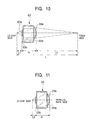
- an aspheric lens 23 having high NA and short WD is mounted on a silicon substrate 55.
- the aspheric lens 23 consists of an infinite-type lens of optical glass and comprises a lens main body 23a provided with double convex aspheric surfaces and an edge portion 23b in the periphery of the lens main body 23a, the outer diameter ( ⁇ ) being 1.0 mm, the lens thickness (tc) being 0.81 mm, the focal distance (L2) being infinite, the NA (numerical aperture) being 0.60.
- an optical semiconductor device comprising a silicon substrate having on one side a V-shaped first groove portion formed by etching, an optical element having an optical axis in the direction of the first groove portion and mounted to this side, and a lens mounted in the first groove portion, wherein the first groove portion comprises first and second opposing inclined surfaces and a third inclined surface perpendicular to the first and second inclined surfaces, wherein there is formed in the silicon substrate a second groove portion extending in a direction perpendicular to the direction of the first groove portion and formed by cutting so as to include the first through third inclined surfaces, and wherein the lens is mounted to the first and second inclined surfaces, with a part thereof protruding in the second groove portion, the optical element being capable of optical communication through the lens.
- an optical semiconductor device wherein the second groove portion is formed as a recess extending across the silicon substrate.
- an optical semiconductor device wherein an edge portion of the lens abuts the side wall of the second groove portion.
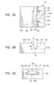
- the optical semiconductor device 10 is provided with a silicon substrate 15 having a first groove portion 15b of a substantially V-shaped (trapezoidal) configuration formed in the upper surface portion (one side) thereof.
- the silicon substrate 15 consists of a silicon (Si) single crystal, and the upper surface portion 15a thereof has a (111) crystal surface, the surface of the first groove portion 15b having a (100) crystal surface.
- the first groove portion 15b comprises a rectangular small bottom surface 15d, a first inclined surface 15e and a second inclined surface 15f surrounding the small bottom surface 15d and opposing to each other, and a third inclined surface 15g perpendicular to the first and second inclined surfaces 15e and 15f.
- the first through third inclined surfaces 15e, 15f and 15g which are the (100) crystal surfaces of the first groove portion 15b are formed by performing anisotropic etching on the (111) crystal surface of the upper surface portion 15a by using a resist mask formed by photolithography.
- a recessed slit (second groove portion) 15k formed by cutting so as to include the first, second and third inclined surfaces 15e, 15f and 15g.
- this slit 15k there is formed a side wall 15j which is perpendicular to the upper surface portion 15a and the small bottom surface 15d.
- the upper surface portion 15a comprises a large first region 15m adjacent to the third inclined surface 15g, and small second and third regions 15n and 15p respectively adjacent to the first and second inclined surfaces 15e and 15f.
- a light emitting element 11 such as a semiconductor laser or the like, which is an optical element.
- This light emitting element 11 is arranged on the first region 15m and close to the edge portion of the third inclined surface 15g, the optical axis of the light 12 emitted from the end surface thereof being in the direction along the firs and second inclined surfaces 15e and 15f of the first groove portion 15b.
- an aspheric lens 23 (See Fig. 11) of high NA (numeric aperture).
- the positioning of the aspheric lens 23 is effected by the first and second inclined surfaces 15e and 15f, and it is mounted and fixed such that its optical axis coincides with the optical axis of the light emitting element 11.
- the aspheric lens 23 is mounted and fixed in the first groove portion 15b and the slit 15k close to the light emitting element 11 side, that is, in a condition in which the working distance (WD) is short, without generating any interfering portion (H) .
- the silicon substrate 15 shown in Figs. 5A through 5C is prepared.
- anisopropic etching is performed on the upper surface of the substrate consisting of silicon single crystal, thereby forming a substantially V-shaped (trapezoidal) first groove portion 15b.
- the inclination angle ( ⁇ 1, ⁇ 2, and ⁇ 3) of the first through third inclined surfaces 15e, 15f and 15g are all 54.7 degrees.
- the light emitting element 11 and the high NA aspheric lens 23 are placed on the silicon substrate 15.
- the light emitting element 11 is accurately optical-axis-adjusted and mounted and fixed to the first region 15m of the upper surface portion 15a by a jig (not shown).
- the edge portion 23b of the aspheric lens 23 is positioned in the direction perpendicular to the optical axis by the first and second inclined surfaces 15e and 15f. That is, positioning and adjustment is effected in the horizontal direction (X-axis direction) and the vertical direction (Y-axis direction). Further, along the optical axis direction, the positioning (Z-axis direction) of the aspheric lens 23 is effected by moving it from the first and second inclined surfaces 15e and 15f to the slit 15k and the third inclined surface 15g while effecting optical adjustment, and it mounted and fixed to predetermined positions of the first groove portion 15b and the slit 15k of the silicon substrate 15.
- the operation of the optical semiconductor device 10, constructed and assembled as described above, will be illustrated.
- the light 12 radiated from the end surface of the light emitting element 11 impinges upon a surface of the high NA aspheric lens 23 without being interrupted, and is further emitted from the other surface of the aspheric lens 23 as parallel rays 12'.
- the configuration of the slit 15k thereof is such that it is a recess completely extending across the silicon substrate 15, if there is no interfering portion (H) in the mounting portion of the aspheric lens 23, there is no need to completely extend across the silicon substrate 15.
- the slit may be formed in the configuration shown in Fig. 6.
- the section of the slit 15k' of the silicon 15 formed has a sectional configuration such that it is recessed in the direction perpendicular to the optical axis direction and curved in the optical axis direction.
- portions of the first, second and third regions 15m, 15n and 15p of the upper surface portion 15a are connected to each other.
- the aspheric lens 23 While in the optical semiconductor device 10 the high NA aspheric lens 23 is mounted, this should not be construed restrictively. It is also applicable to an aspheric lens of an optical system in which it is necessary to avoid the interfering portion in the prior art.
- the aspheric lens may be a finite system in which the outer diameter ( ⁇ ) is 1.0 mm, the lens thickness (tc) is 0.81, the optical length (L) is 3.98 mm, the focal distance (f) is approximately 2.91 mm, the NA (numerical aperture) is 0.5, magnification (m) is 5, and the distance (L1) from the object point to the apex of the lens surface is 0.25.
- optical semiconductor device 10 is a transmission side optical semiconductor device in which the light emitting element 11 is mounted, it may also be a reception side optical semiconductor device in which a photo detector (optical element) such as a photo diode is incorporated.
- the positioning of the optical semiconductor device 10 may be effected by causing the side wall 15j formed by cutting a part of the third inclined surface 15g of the silicon substrate 15 against the edge portion 23b of the aspheric lens 23.
- the optical semiconductor device 10 constructed as described above, has the following advantages.
- an optical semiconductor device comprising a silicon substrate having on one side a V-shaped first groove portion formed by etching, an optical element having an optical axis in the direction of the first groove portion and mounted to this side, and a lens mounted in the first groove portion, wherein the first groove portion comprises first and second opposing inclined surfaces and a third inclined surface perpendicular to the first and second inclined surfaces, wherein there is formed in the silicon substrate a second groove portion extending in a direction perpendicular to the direction of the first groove portion and formed by cutting so as to include the first through third inclined surfaces, and wherein the lens is mounted to the first and second inclined surfaces, with a part thereof protruding in the second groove portion, the optical element being capable of optical communication through the lens, whereby it is possible to mount the lens to a desired position in the vicinity of the optical element, so that it is possible to effect mounting on the silicon substrate with the lens being of high NA and utilizing the characteristics of the short WD lens.
- this optical semiconductor device it is possible to achieve an enhancement in efficiency in optical coupling in conformity with the increase in speed and capacitance in optical communication.
- the second groove portion is formed as a recess extending across the silicon substrate, whereby the machining is effected solely by cutting in one direction, so that the machining can be effected easily and accurately.
- an edge portion of the lens abuts the side wall of the second groove portion, whereby, due to the side wall, the positioning in the optical axis (Z-axis) direction is possible, so that the optical adjustment at the time of mounting the lens can be effected easily, and the positioning and fixing can be effected more accurately.
Landscapes
- Physics & Mathematics (AREA)
- General Physics & Mathematics (AREA)
- Optics & Photonics (AREA)
- Condensed Matter Physics & Semiconductors (AREA)
- Electromagnetism (AREA)
- Optical Couplings Of Light Guides (AREA)
- Led Devices (AREA)
- Semiconductor Lasers (AREA)
- Led Device Packages (AREA)
- Light Receiving Elements (AREA)
Abstract
Description
Claims (3)
- An optical semiconductor device comprising a silicon substrate having on one side a V-shaped first groove portion formed by etching, an optical element having an optical axis in the direction of the first groove portion and mounted to this side, and a lens mounted in the first groove portion,wherein the first groove portion comprises first and second opposing inclined surfaces and a third inclined surface perpendicular to the first and second inclined surfaces,wherein there is formed in the silicon substrate a second groove portion extending in a direction perpendicular to the direction of the first groove portion and formed by cutting so as to include the first through third inclined surfaces, andwherein the lens is mounted to the first and second inclined surfaces, with a part thereof protruding in the second groove portion, the optical element being capable of optical communication through the lens.
- An optical semiconductor device according to Claim 1, wherein the second groove portion is formed as a recess extending across the silicon substrate.
- An optical semiconductor device according to Claim 1, wherein an edge portion of the lens abuts the side wall of the second groove portion.
Applications Claiming Priority (2)
| Application Number | Priority Date | Filing Date | Title |
|---|---|---|---|
| JP2000056013 | 2000-02-28 | ||
| JP2000056013A JP2001242357A (en) | 2000-02-28 | 2000-02-28 | Optical semiconductor device |
Publications (2)
| Publication Number | Publication Date |
|---|---|
| EP1136862A2 true EP1136862A2 (en) | 2001-09-26 |
| EP1136862A3 EP1136862A3 (en) | 2004-06-23 |
Family
ID=18577043
Family Applications (1)
| Application Number | Title | Priority Date | Filing Date |
|---|---|---|---|
| EP01100598A Withdrawn EP1136862A3 (en) | 2000-02-28 | 2001-01-10 | Optical semiconductor device provided with high numerical aperture lens |
Country Status (3)
| Country | Link |
|---|---|
| US (2) | US6625188B2 (en) |
| EP (1) | EP1136862A3 (en) |
| JP (1) | JP2001242357A (en) |
Families Citing this family (13)
| Publication number | Priority date | Publication date | Assignee | Title |
|---|---|---|---|---|
| DE10042904C2 (en) * | 2000-08-31 | 2003-03-13 | Infineon Technologies Ag | Semiconductor laser chip with integrated beam former and method for producing a semiconductor laser chip with integrated beam former |
| JP2003303975A (en) * | 2002-04-08 | 2003-10-24 | Opnext Japan Inc | Optical module with monitor photodiode. |
| JP2007286211A (en) * | 2006-04-14 | 2007-11-01 | Alps Electric Co Ltd | Optical member and optical communication module |
| JP5172113B2 (en) * | 2006-07-19 | 2013-03-27 | 新日本無線株式会社 | Manufacturing method of light emitting / receiving element |
| US9018561B2 (en) * | 2007-05-23 | 2015-04-28 | Cymer, Llc | High power seed/amplifier laser system with beam shaping intermediate the seed and amplifier |
| US8490678B2 (en) * | 2008-06-02 | 2013-07-23 | Gerald Ho Kim | Silicon-based thermal energy transfer device and apparatus |
| US8238401B2 (en) * | 2008-08-25 | 2012-08-07 | Gerald Ho Kim | Silicon-based lens support structure for diode laser |
| USD630666S1 (en) * | 2008-12-23 | 2011-01-11 | Alps Electric Co., Ltd. | Lens for light communication |
| WO2010116862A1 (en) * | 2009-03-30 | 2010-10-14 | アルプス電気株式会社 | Collimating lens |
| JP1552762S (en) * | 2015-10-30 | 2016-06-27 | ||
| JP1552852S (en) * | 2015-10-30 | 2016-06-27 | ||
| JP1557566S (en) * | 2015-10-30 | 2016-08-29 | ||
| DE102017123798B4 (en) | 2017-10-12 | 2022-03-03 | OSRAM Opto Semiconductors Gesellschaft mit beschränkter Haftung | Semiconductor lasers and manufacturing processes for optoelectronic semiconductor components |
Family Cites Families (10)
| Publication number | Priority date | Publication date | Assignee | Title |
|---|---|---|---|---|
| US5555333A (en) * | 1993-07-12 | 1996-09-10 | Ricoh Company, Ltd. | Optical module and a fabrication process thereof |
| JPH07199006A (en) * | 1994-01-11 | 1995-08-04 | Hitachi Ltd | Optical subassembly and optical module |
| DE69514358T2 (en) * | 1994-06-29 | 2000-08-24 | British Telecommunications Public Ltd. Co., London | OPTICAL COMPONENT ARRANGEMENT |
| JP3853866B2 (en) * | 1995-02-21 | 2006-12-06 | 日本碍子株式会社 | Optical fiber fixing substrate |
| JP3592406B2 (en) * | 1995-07-10 | 2004-11-24 | 富士通株式会社 | Optical module and method for manufacturing optical module |
| US5706371A (en) * | 1996-12-03 | 1998-01-06 | E-Tek Dynamics, Inc. | Optical isolator array device |
| US5870417A (en) * | 1996-12-20 | 1999-02-09 | Sdl, Inc. | Thermal compensators for waveguide DBR laser sources |
| JPH11264920A (en) * | 1998-03-18 | 1999-09-28 | Fujitsu Ltd | Optical transmission module |
| JP3429190B2 (en) | 1998-04-10 | 2003-07-22 | 株式会社日立製作所 | Optical semiconductor device |
| US6172997B1 (en) * | 1998-06-16 | 2001-01-09 | Aculight Corporation | Integrated semiconductor diode laser pumped solid state laser |
-
2000
- 2000-02-28 JP JP2000056013A patent/JP2001242357A/en not_active Withdrawn
-
2001
- 2001-01-10 EP EP01100598A patent/EP1136862A3/en not_active Withdrawn
- 2001-02-15 US US09/784,592 patent/US6625188B2/en not_active Expired - Fee Related
-
2003
- 2003-06-26 US US10/607,475 patent/US6813294B2/en not_active Expired - Fee Related
Also Published As
| Publication number | Publication date |
|---|---|
| US6625188B2 (en) | 2003-09-23 |
| US6813294B2 (en) | 2004-11-02 |
| US20040013140A1 (en) | 2004-01-22 |
| EP1136862A3 (en) | 2004-06-23 |
| JP2001242357A (en) | 2001-09-07 |
| US20010030984A1 (en) | 2001-10-18 |
Similar Documents
| Publication | Publication Date | Title |
|---|---|---|
| US5552918A (en) | Transmission and reception module for a bidirectional optical communication and signal transmission | |
| US6625188B2 (en) | Optical semiconductor device provided with high-NA lens | |
| US6311894B1 (en) | Optical scanning device having a reflection section and photodetecting section integrally formed on a moving part of an optical scanning section | |
| US4611883A (en) | Two-dimensional optics element for correcting aberrations | |
| WO2012108545A1 (en) | Optical module having enhanced optical coupling efficiency between laser diode and optical fiber | |
| EP0826993A1 (en) | Optoelectronics module | |
| US20040101246A1 (en) | Optical via for three dimensional interconnection | |
| JP3495493B2 (en) | Light emitting module | |
| JP2007212795A (en) | Optical semiconductor module, adjustment method therefor and manufacturing method therefor | |
| JP2000028865A (en) | Semiconductor laser module | |
| JPH0519195A (en) | Optical device | |
| JPH09218324A (en) | Light emission module | |
| US20210026080A1 (en) | Optical receptacle and optical transceiver | |
| JPS63182617A (en) | optical device | |
| GB2295265A (en) | Injection laser assembly incorporating a monitor photosensor | |
| JPH11295559A (en) | Semiconductor laser module | |
| JPH08146250A (en) | Condensing lens and manufacturing method thereof | |
| US20060045423A1 (en) | Diffractive coupler optimized for alignment tolerances | |
| JPH0667069A (en) | Photosemiconductor device | |
| JP2004333885A (en) | Optical device and lens member used for the same | |
| JP2001133714A (en) | Optical scanning optical system | |
| JPH02106707A (en) | Optical circuit device | |
| JP2000304964A (en) | Optical coupling device | |
| JP2000101516A (en) | Transmission/reception integrated optical communication equipment | |
| JPH10239564A (en) | Optical module |
Legal Events
| Date | Code | Title | Description |
|---|---|---|---|
| PUAI | Public reference made under article 153(3) epc to a published international application that has entered the european phase |
Free format text: ORIGINAL CODE: 0009012 |
|
| AK | Designated contracting states |
Kind code of ref document: A2 Designated state(s): AT BE CH CY DE DK ES FI FR GB GR IE IT LI LU MC NL PT SE TR |
|
| AX | Request for extension of the european patent |
Free format text: AL;LT;LV;MK;RO;SI |
|
| PUAL | Search report despatched |
Free format text: ORIGINAL CODE: 0009013 |
|
| AK | Designated contracting states |
Kind code of ref document: A3 Designated state(s): AT BE CH CY DE DK ES FI FR GB GR IE IT LI LU MC NL PT SE TR |
|
| AX | Request for extension of the european patent |
Extension state: AL LT LV MK RO SI |
|
| 17P | Request for examination filed |
Effective date: 20040713 |
|
| AKX | Designation fees paid |
Designated state(s): DE FR GB |
|
| STAA | Information on the status of an ep patent application or granted ep patent |
Free format text: STATUS: THE APPLICATION IS DEEMED TO BE WITHDRAWN |
|
| 18D | Application deemed to be withdrawn |
Effective date: 20060223 |