EP1134617A2 - Pattern formation material and method - Google Patents
Pattern formation material and method Download PDFInfo
- Publication number
- EP1134617A2 EP1134617A2 EP01105830A EP01105830A EP1134617A2 EP 1134617 A2 EP1134617 A2 EP 1134617A2 EP 01105830 A EP01105830 A EP 01105830A EP 01105830 A EP01105830 A EP 01105830A EP 1134617 A2 EP1134617 A2 EP 1134617A2
- Authority
- EP
- European Patent Office
- Prior art keywords
- chemical formula
- pattern formation
- unit represented
- resist film
- chlorine atom
- Prior art date
- Legal status (The legal status is an assumption and is not a legal conclusion. Google has not performed a legal analysis and makes no representation as to the accuracy of the status listed.)
- Withdrawn
Links
Images


Classifications
-
- G—PHYSICS
- G03—PHOTOGRAPHY; CINEMATOGRAPHY; ANALOGOUS TECHNIQUES USING WAVES OTHER THAN OPTICAL WAVES; ELECTROGRAPHY; HOLOGRAPHY
- G03F—PHOTOMECHANICAL PRODUCTION OF TEXTURED OR PATTERNED SURFACES, e.g. FOR PRINTING, FOR PROCESSING OF SEMICONDUCTOR DEVICES; MATERIALS THEREFOR; ORIGINALS THEREFOR; APPARATUS SPECIALLY ADAPTED THEREFOR
- G03F7/00—Photomechanical, e.g. photolithographic, production of textured or patterned surfaces, e.g. printing surfaces; Materials therefor, e.g. comprising photoresists; Apparatus specially adapted therefor
- G03F7/004—Photosensitive materials
- G03F7/027—Non-macromolecular photopolymerisable compounds having carbon-to-carbon double bonds, e.g. ethylenic compounds
- G03F7/028—Non-macromolecular photopolymerisable compounds having carbon-to-carbon double bonds, e.g. ethylenic compounds with photosensitivity-increasing substances, e.g. photoinitiators
-
- G—PHYSICS
- G03—PHOTOGRAPHY; CINEMATOGRAPHY; ANALOGOUS TECHNIQUES USING WAVES OTHER THAN OPTICAL WAVES; ELECTROGRAPHY; HOLOGRAPHY
- G03F—PHOTOMECHANICAL PRODUCTION OF TEXTURED OR PATTERNED SURFACES, e.g. FOR PRINTING, FOR PROCESSING OF SEMICONDUCTOR DEVICES; MATERIALS THEREFOR; ORIGINALS THEREFOR; APPARATUS SPECIALLY ADAPTED THEREFOR
- G03F7/00—Photomechanical, e.g. photolithographic, production of textured or patterned surfaces, e.g. printing surfaces; Materials therefor, e.g. comprising photoresists; Apparatus specially adapted therefor
- G03F7/004—Photosensitive materials
- G03F7/0045—Photosensitive materials with organic non-macromolecular light-sensitive compounds not otherwise provided for, e.g. dissolution inhibitors
-
- G—PHYSICS
- G03—PHOTOGRAPHY; CINEMATOGRAPHY; ANALOGOUS TECHNIQUES USING WAVES OTHER THAN OPTICAL WAVES; ELECTROGRAPHY; HOLOGRAPHY
- G03F—PHOTOMECHANICAL PRODUCTION OF TEXTURED OR PATTERNED SURFACES, e.g. FOR PRINTING, FOR PROCESSING OF SEMICONDUCTOR DEVICES; MATERIALS THEREFOR; ORIGINALS THEREFOR; APPARATUS SPECIALLY ADAPTED THEREFOR
- G03F7/00—Photomechanical, e.g. photolithographic, production of textured or patterned surfaces, e.g. printing surfaces; Materials therefor, e.g. comprising photoresists; Apparatus specially adapted therefor
- G03F7/004—Photosensitive materials
- G03F7/039—Macromolecular compounds which are photodegradable, e.g. positive electron resists
-
- Y—GENERAL TAGGING OF NEW TECHNOLOGICAL DEVELOPMENTS; GENERAL TAGGING OF CROSS-SECTIONAL TECHNOLOGIES SPANNING OVER SEVERAL SECTIONS OF THE IPC; TECHNICAL SUBJECTS COVERED BY FORMER USPC CROSS-REFERENCE ART COLLECTIONS [XRACs] AND DIGESTS
- Y10—TECHNICAL SUBJECTS COVERED BY FORMER USPC
- Y10S—TECHNICAL SUBJECTS COVERED BY FORMER USPC CROSS-REFERENCE ART COLLECTIONS [XRACs] AND DIGESTS
- Y10S430/00—Radiation imagery chemistry: process, composition, or product thereof
- Y10S430/1053—Imaging affecting physical property or radiation sensitive material, or producing nonplanar or printing surface - process, composition, or product: radiation sensitive composition or product or process of making binder containing
- Y10S430/1055—Radiation sensitive composition or product or process of making
- Y10S430/106—Binder containing
-
- Y—GENERAL TAGGING OF NEW TECHNOLOGICAL DEVELOPMENTS; GENERAL TAGGING OF CROSS-SECTIONAL TECHNOLOGIES SPANNING OVER SEVERAL SECTIONS OF THE IPC; TECHNICAL SUBJECTS COVERED BY FORMER USPC CROSS-REFERENCE ART COLLECTIONS [XRACs] AND DIGESTS
- Y10—TECHNICAL SUBJECTS COVERED BY FORMER USPC
- Y10S—TECHNICAL SUBJECTS COVERED BY FORMER USPC CROSS-REFERENCE ART COLLECTIONS [XRACs] AND DIGESTS
- Y10S430/00—Radiation imagery chemistry: process, composition, or product thereof
- Y10S430/1053—Imaging affecting physical property or radiation sensitive material, or producing nonplanar or printing surface - process, composition, or product: radiation sensitive composition or product or process of making binder containing
- Y10S430/1055—Radiation sensitive composition or product or process of making
- Y10S430/106—Binder containing
- Y10S430/11—Vinyl alcohol polymer or derivative
-
- Y—GENERAL TAGGING OF NEW TECHNOLOGICAL DEVELOPMENTS; GENERAL TAGGING OF CROSS-SECTIONAL TECHNOLOGIES SPANNING OVER SEVERAL SECTIONS OF THE IPC; TECHNICAL SUBJECTS COVERED BY FORMER USPC CROSS-REFERENCE ART COLLECTIONS [XRACs] AND DIGESTS
- Y10—TECHNICAL SUBJECTS COVERED BY FORMER USPC
- Y10S—TECHNICAL SUBJECTS COVERED BY FORMER USPC CROSS-REFERENCE ART COLLECTIONS [XRACs] AND DIGESTS
- Y10S430/00—Radiation imagery chemistry: process, composition, or product thereof
- Y10S430/1053—Imaging affecting physical property or radiation sensitive material, or producing nonplanar or printing surface - process, composition, or product: radiation sensitive composition or product or process of making binder containing
- Y10S430/1055—Radiation sensitive composition or product or process of making
- Y10S430/106—Binder containing
- Y10S430/111—Polymer of unsaturated acid or ester
-
- Y—GENERAL TAGGING OF NEW TECHNOLOGICAL DEVELOPMENTS; GENERAL TAGGING OF CROSS-SECTIONAL TECHNOLOGIES SPANNING OVER SEVERAL SECTIONS OF THE IPC; TECHNICAL SUBJECTS COVERED BY FORMER USPC CROSS-REFERENCE ART COLLECTIONS [XRACs] AND DIGESTS
- Y10—TECHNICAL SUBJECTS COVERED BY FORMER USPC
- Y10S—TECHNICAL SUBJECTS COVERED BY FORMER USPC CROSS-REFERENCE ART COLLECTIONS [XRACs] AND DIGESTS
- Y10S430/00—Radiation imagery chemistry: process, composition, or product thereof
- Y10S430/1053—Imaging affecting physical property or radiation sensitive material, or producing nonplanar or printing surface - process, composition, or product: radiation sensitive composition or product or process of making binder containing
- Y10S430/1055—Radiation sensitive composition or product or process of making
- Y10S430/114—Initiator containing
- Y10S430/115—Cationic or anionic
-
- Y—GENERAL TAGGING OF NEW TECHNOLOGICAL DEVELOPMENTS; GENERAL TAGGING OF CROSS-SECTIONAL TECHNOLOGIES SPANNING OVER SEVERAL SECTIONS OF THE IPC; TECHNICAL SUBJECTS COVERED BY FORMER USPC CROSS-REFERENCE ART COLLECTIONS [XRACs] AND DIGESTS
- Y10—TECHNICAL SUBJECTS COVERED BY FORMER USPC
- Y10S—TECHNICAL SUBJECTS COVERED BY FORMER USPC CROSS-REFERENCE ART COLLECTIONS [XRACs] AND DIGESTS
- Y10S430/00—Radiation imagery chemistry: process, composition, or product thereof
- Y10S430/146—Laser beam
Definitions
- the present invention relates to pattern formation material and method. More particularly, it relates to a pattern formation method employed for forming a resist pattern, used for forming a semiconductor device or a semiconductor integrated circuit on a semiconductor substrate, by using exposing light of a wavelength of a 1 nm through 30 nm band or a 110 nm through 180 nm band, and a pattern formation material used in the same.
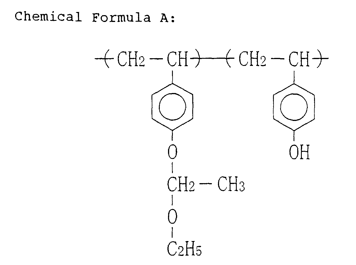
- a resist pattern is formed by using a chemically amplified resist material including a polyhydroxystyrene derivative and an acid generator as principal constituents with KrF excimer laser (of a wavelength of a 248 nm band) used as exposing light.
- the resist film 2 is developed with an alkaline developer, thereby forming a resist pattern 5.
- the present inventors have studied the causes of the conventional problems occurring in using the aforementioned conventional chemically amplified resist materials, and have found the following:
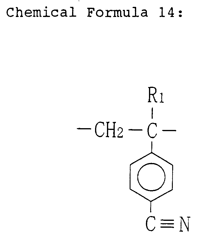
- the transmittance against light of a wavelength of a 1 nm through 180 nm band can be improved, and since an alkyl group, a chlorine atom or an alkyl group including a chlorine atom is substituted for a hydrogen atom located at the ⁇ -position of the principal chain of each of the first and second units, a crosslinking reaction is never caused in the principal chains, resulting in improving the solubility of an exposed portion of a resist film in a developer.
- the first unit has a benzene ring, the dry etching resistance can be improved.
- carboxylic acid is generated in the exposed portion of the resist film. Therefore, the contrast between the exposed portion and an unexposed portion can be improved.
- the fifth pattern formation method of this invention comprises the steps of forming a resist film by applying, on a substrate, the fifth pattern formation material; irradiating the resist film with exposing light of a wavelength of a 1 nm through 30 nm band or a 110 nm through 180 nm band for pattern exposure; and forming a resist pattern by developing the resist film after the pattern exposure.
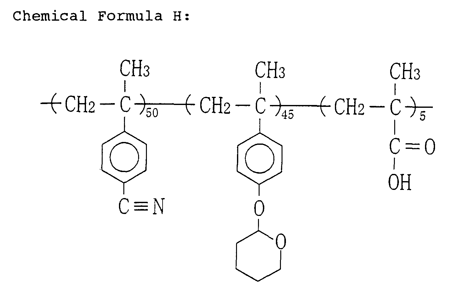
- the fifth pattern formation material is used, and hence, the transmittance against light of a wavelength of a 1 nm through 180 nm band can be improved and the solubility of an exposed portion of the resist film in a developer can be improved. Furthermore, the dry etching resistance can be largely improved. In addition, the wettability of the pattern formation material is improved so as to improve the adhesion onto the substrate, and the dissolving rate in an alkaline developer can be controlled by adjusting the ratio of the third unit in the polymer. Moreover, since carboxylic acid is generated in the exposed portion of the resist film through irradiation with light, the contrast between the exposed portion and an unexposed portion can be improved.
- Embodiment 3 is different from Embodiment 1 in the resist material alone, and hence, the resist material alone will be herein described.
- Embodiment 5 is different from Embodiment 1 in the resist material alone, and hence, the resist material alone will be herein described.
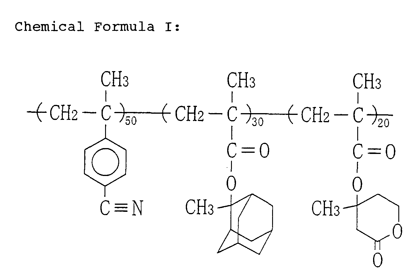
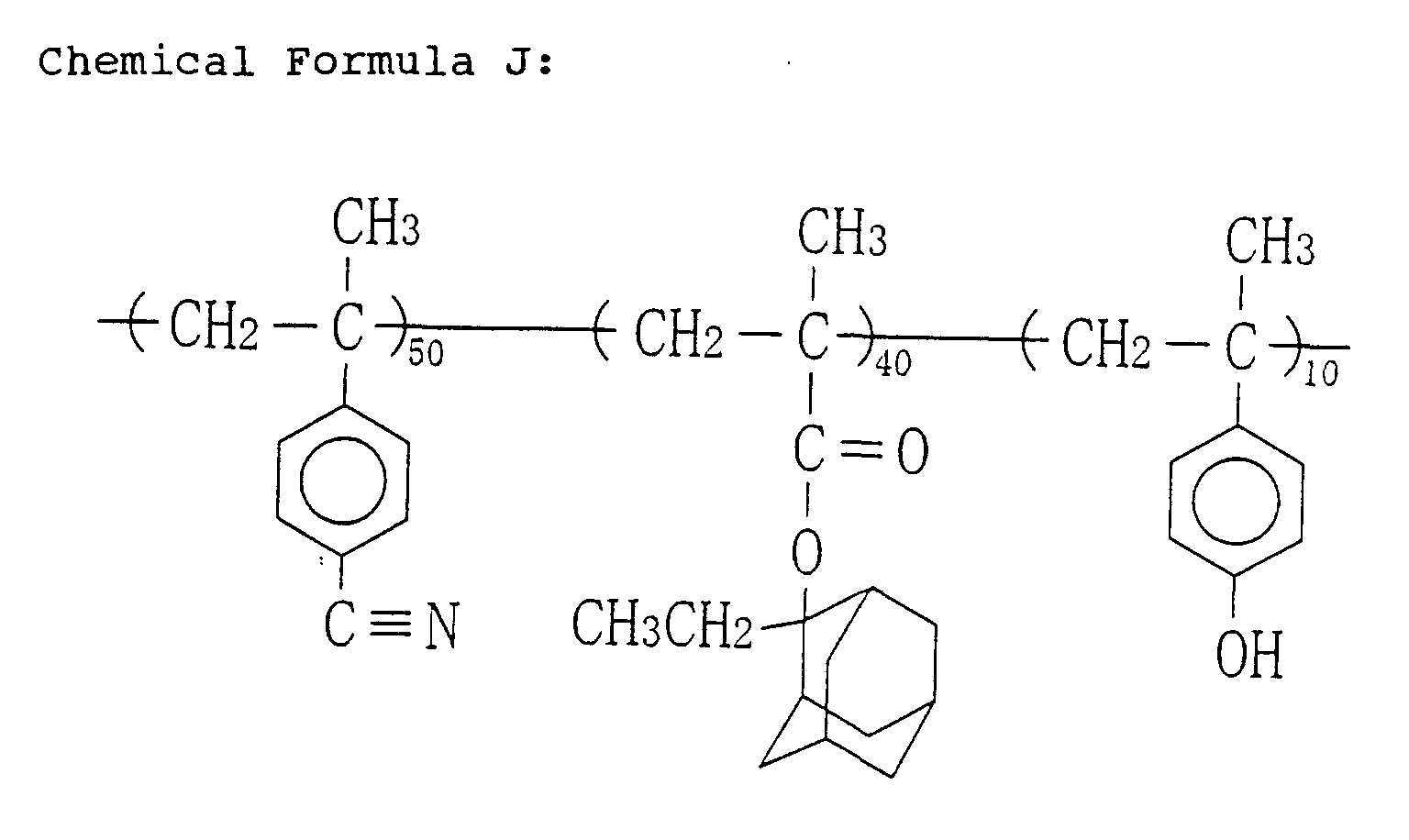
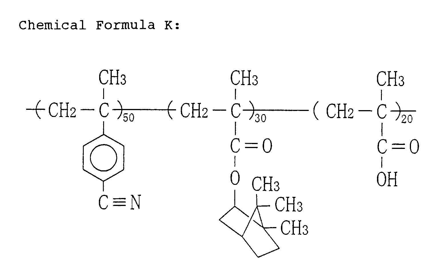
- the fifth pattern formation material and the fifth pattern formation method described above are embodied, and the specific composition of the resist material is as follows:
- Embodiment 6 is different from Embodiment 1 in the resist material alone, and hence, the resist material alone will be herein described.
Landscapes
- Physics & Mathematics (AREA)
- Spectroscopy & Molecular Physics (AREA)
- General Physics & Mathematics (AREA)
- Materials For Photolithography (AREA)
- Addition Polymer Or Copolymer, Post-Treatments, Or Chemical Modifications (AREA)
- Exposure And Positioning Against Photoresist Photosensitive Materials (AREA)
- Photosensitive Polymer And Photoresist Processing (AREA)
Abstract

Description












Claims (18)
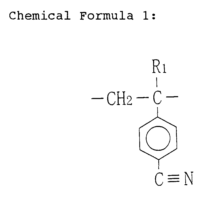
- A pattern formation material comprising:a polymer including a first unit represented by Chemical Formula 1 and a second unit represented by Chemical Formula 2; andan acid generator,
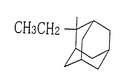
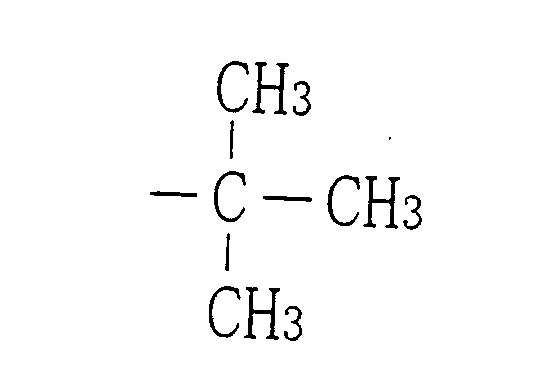
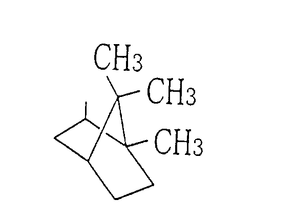
 wherein R1 and R2 are the same or different and selected from the group consisting of an alkyl group, a chlorine atom and an alkyl group including a chlorine atom; and R3 is a protecting group released by an acid.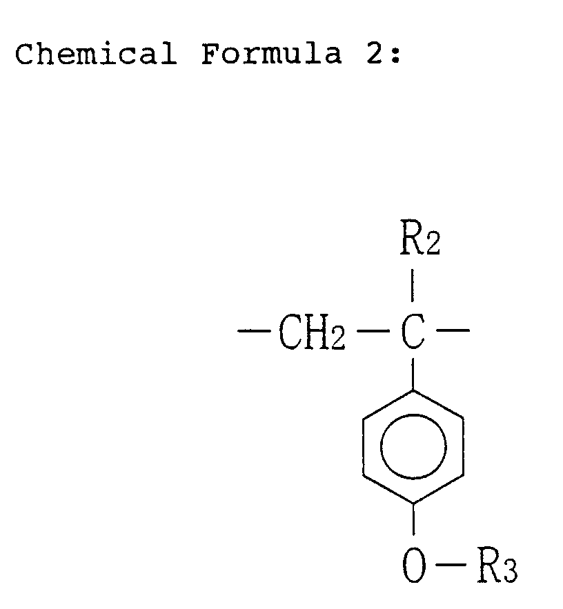
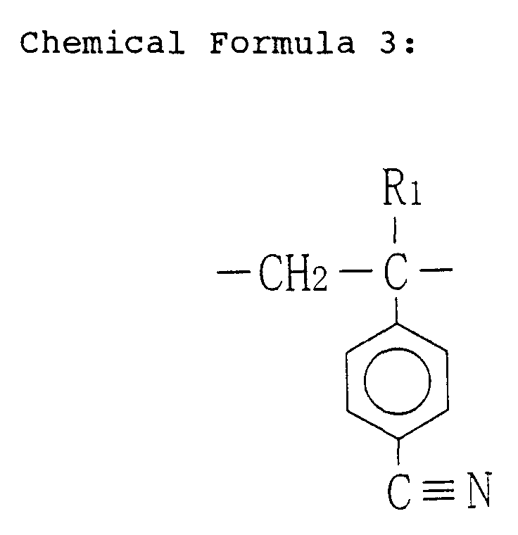
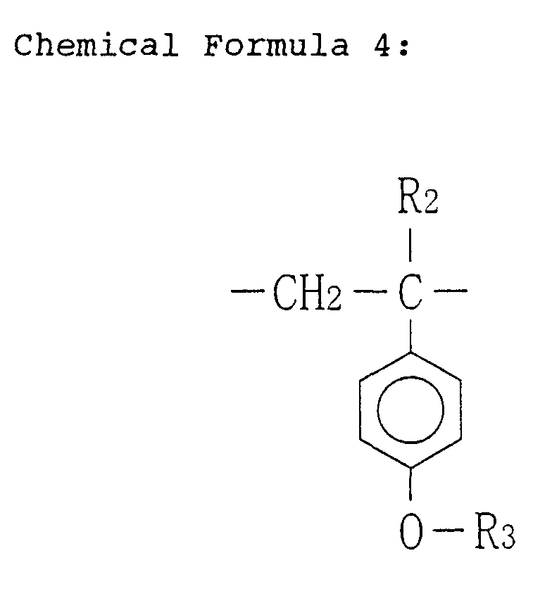
- A pattern formation material comprising:a polymer including a first unit represented by Chemical Formula 3, a second unit represented by Chemical Formula 4 and a third unit represented by Chemical Formula 5; andan acid generator,

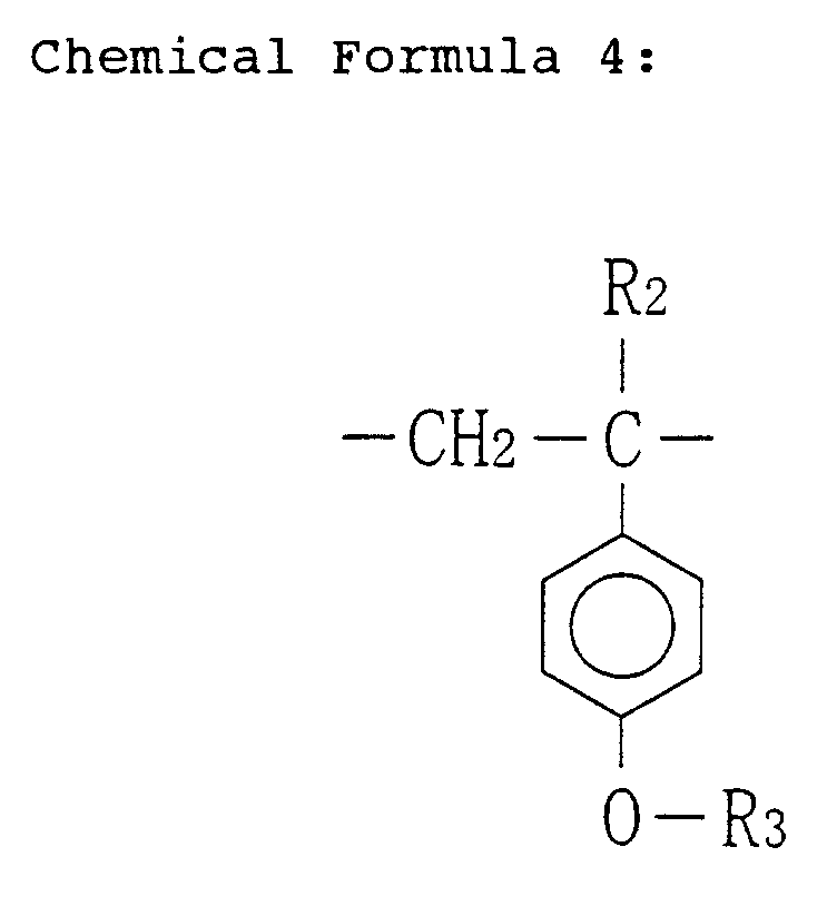 wherein R1, R2 and R4 are the same or different and selected from the group consisting of an alkyl group, a chlorine atom and an alkyl group including a chlorine atom; and R3 is a protecting group released by an acid.
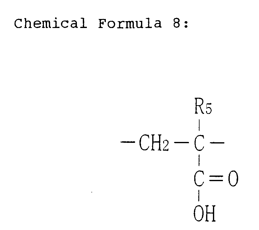
- A pattern formation material comprising:a polymer including a first unit represented by Chemical Formula 6, a second unit represented by Chemical Formula 7 and a third unit represented by Chemical Formula 8; andan acid generator,

 wherein R1, R2 and R5 are the same or different and selected from the group consisting of an alkyl group, a chlorine atom and an alkyl group including a chlorine atom; and R3 is a protecting group released by an acid.
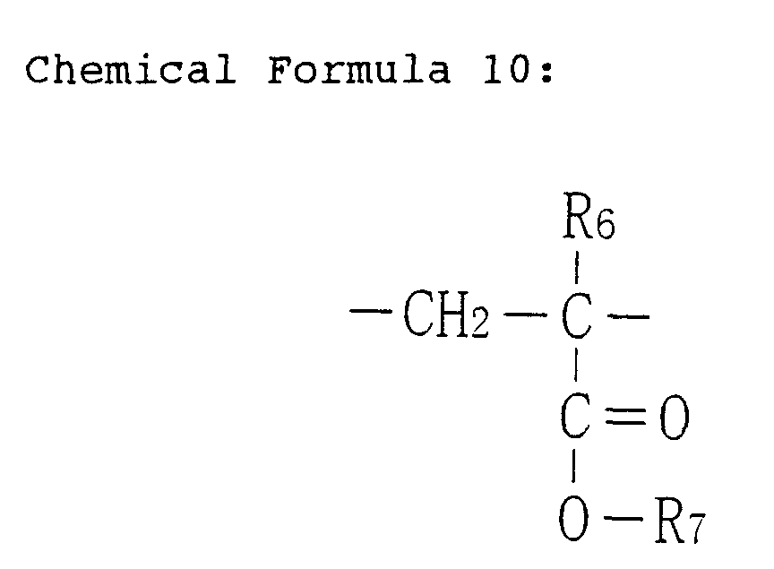
- A pattern formation material comprising:a polymer including a first unit represented by Chemical Formula 9 and a second unit represented by Chemical Formula 10; andan acid generator,
 wherein R1 and R6 are the same or different and selected from the group consisting of an alkyl group, a chlorine atom and an alkyl group including a chlorine atom; and R7 is a protecting group released by an acid.
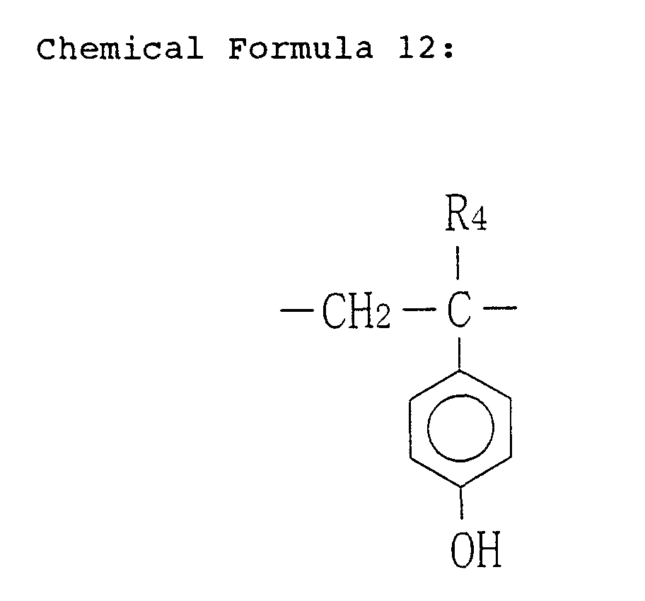
- A pattern formation material comprising:a polymer including a first unit represented by Chemical Formula 11, a second unit represented by Chemical Formula 12 and a third unit represented by Chemical Formula 13; andan acid generator,

 wherein R1, R4 and R6 are the same or different and selected from the group consisting of an alkyl group, a chlorine atom and an alkyl group including a chlorine atom; and R7 is a protecting group released by an acid.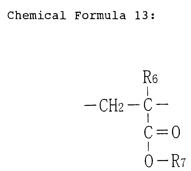
- A pattern formation material comprising:a polymer including a first unit represented by Chemical Formula 14, a second unit represented by Chemical Formula 15 and a third unit represented by Chemical Formula 16; andan acid generator,
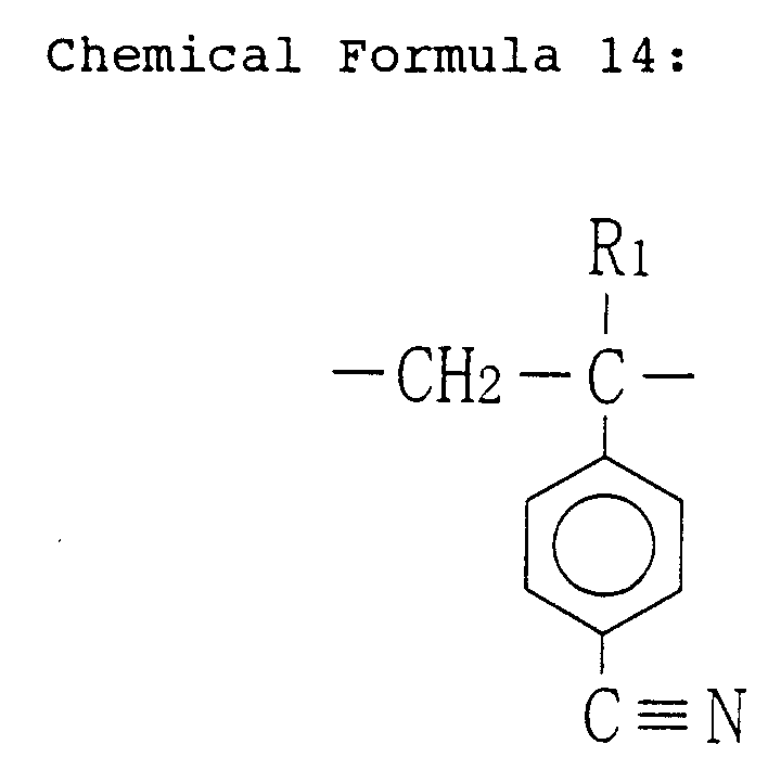
 wherein R1, R5 and R6 are the same or different and selected from the group consisting of an alkyl group, a chlorine atom and an alkyl group including a chlorine atom; and R7 is a protecting group released by an acid.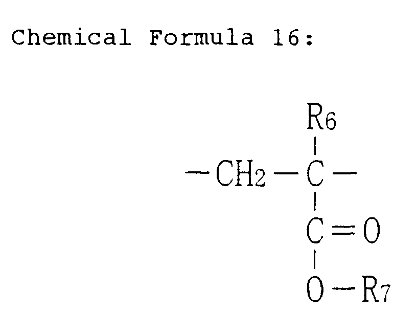
- A pattern formation method comprising the steps of:forming a resist film by applying, on a substrate, a pattern formation material containing a polymer including a first unit represented by Chemical Formula 17 and a second unit represented by Chemical Formula 18, and an acid generator;
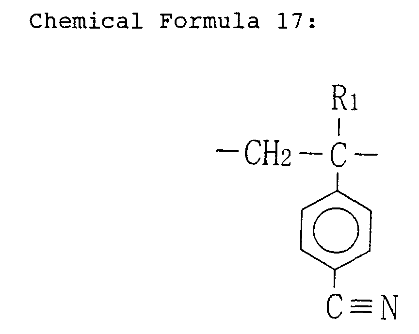 wherein R1 and R2 are the same or different and selected from the group consisting of an alkyl group, a chlorine atom and an alkyl group including a chlorine atom; and R3 is a protecting group released by an acid;
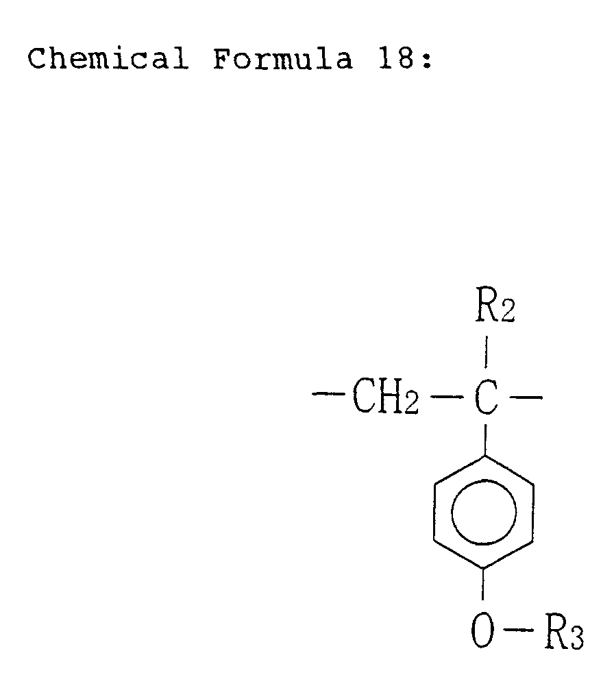 irradiating said resist film with exposing light of a wavelength of a 1 nm through 30 nm band or a 110 nm through 180 nm band for pattern exposure; andforming a resist pattern by developing said resist film after the pattern exposure.
 - The pattern formation method of Claim 7,
wherein said exposing light is F2 excimer laser, Ar2 excimer laser or soft-X rays. - A pattern formation method comprising the steps of:forming a resist film by applying, on a substrate, a pattern formation material containing a polymer including a first unit represented by Chemical Formula 19, a second unit represented by Chemical Formula 20 and a third unit represented by Chemical Formula 21, and an acid generator;

 wherein R1, R2 and R4 are the same or different and selected from the group consisting of an alkyl group, a chlorine atom and an alkyl group including a chlorine atom; and R3 is a protecting group released by an acid;
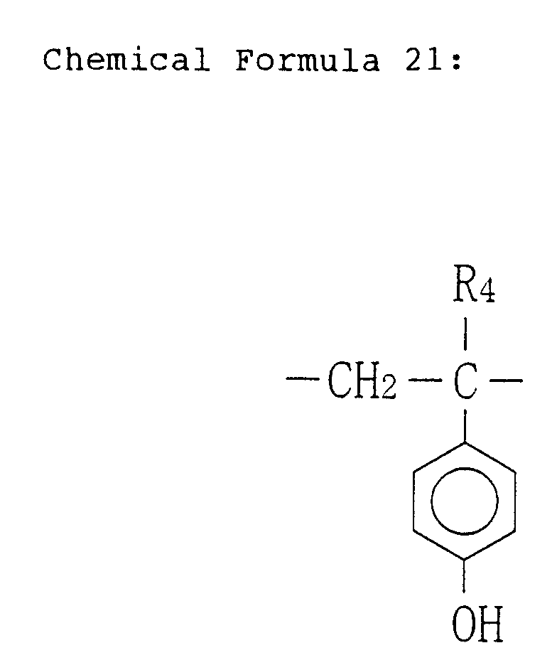 irradiating said resist film with exposing light of a wavelength of a 1 nm through 30 nm band or a 110 nm through 180 nm band for pattern exposure; andforming a resist pattern by developing said resist film after the pattern exposure.
 - The pattern formation method of Claim 9,
wherein said exposing light is F2 excimer laser, Ar2 excimer laser or soft-X rays. - A pattern formation method comprising the steps of:forming a resist film by applying, on a substrate, a pattern formation material containing a polymer including a first unit represented by Chemical Formula 22, a second unit represented by Chemical Formula 23 and a third unit represented by Chemical Formula 24, and an acid generator;

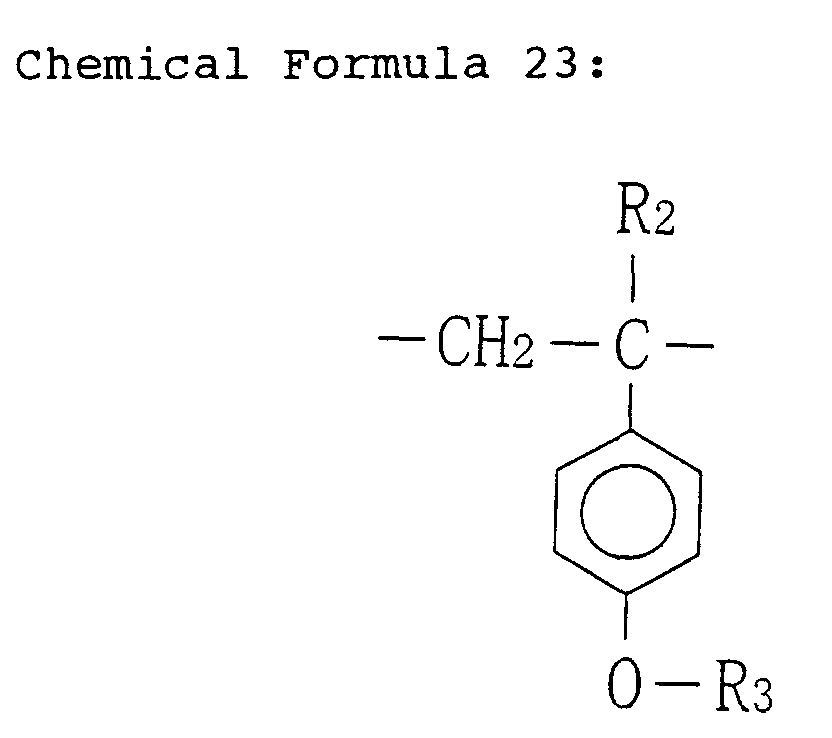 wherein R1, R2 and R5 are the same or different and selected from the group consisting of an alkyl group, a chlorine atom and an alkyl group including a chlorine atom; and R3 is a protecting group released by an acid;
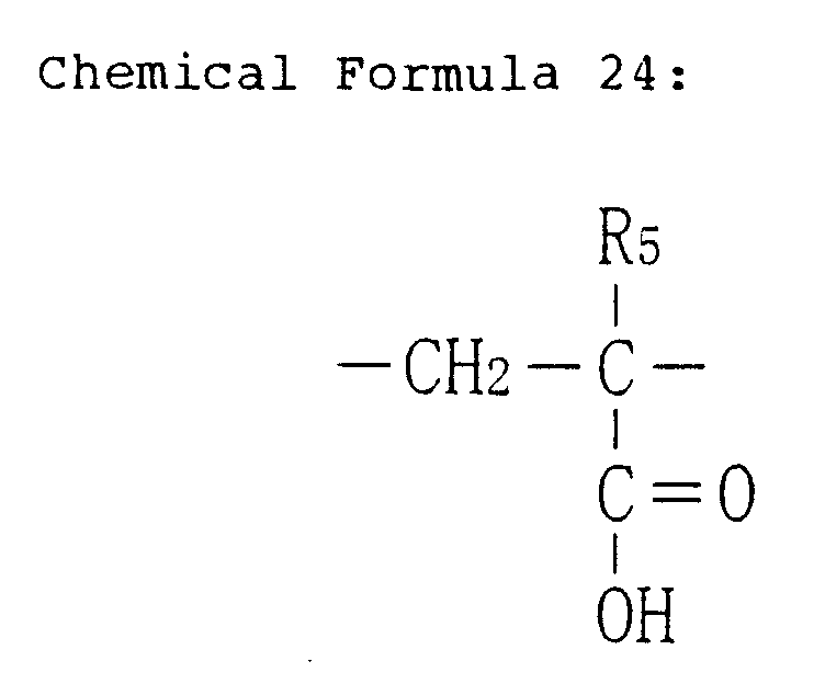 irradiating said resist film with exposing light of a wavelength of a 1 nm through 30 nm band or a 110 nm through 180 nm band for pattern exposure; andforming a resist pattern by developing said resist film after the pattern exposure.
 - The pattern formation method of Claim 11,
wherein said exposing light is F2 excimer laser, Ar2 excimer laser or soft-X rays. - A pattern formation method comprising the steps of:forming a resist film by applying, on a substrate, a pattern formation material containing a polymer including a first unit represented by Chemical Formula 25 and a second unit represented by Chemical Formula 26, and an acid generator;
 wherein R1 and R6 are the same or different and selected from the group consisting of an alkyl group, a chlorine atom and an alkyl group including a chlorine atom; and R7 is a protecting group released by an acid;
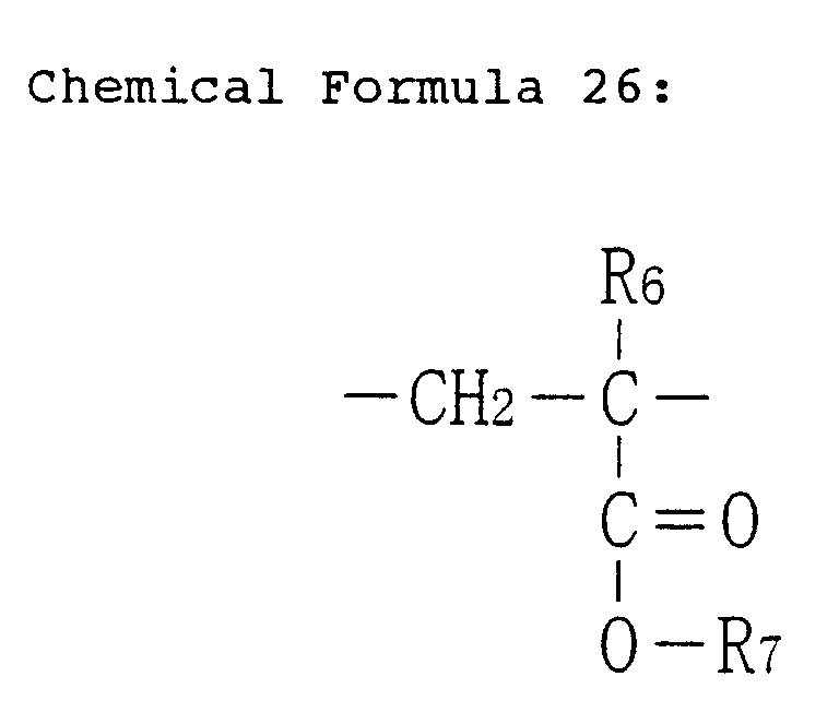 irradiating said resist film with exposing light of a wavelength of a 1 nm through 30 nm band or a 110 nm through 180 nm band for pattern exposure; andforming a resist pattern by developing said resist film after the pattern exposure.
 - The pattern formation method of Claim 13,
wherein said exposing light is F2 excimer laser, Ar2 excimer laser or soft-X rays. - A pattern formation method comprising the steps of:forming a resist film by applying, on a substrate, a pattern formation material containing a polymer including a first unit represented by Chemical Formula 27, a second unit represented by Chemical Formula 28 and a third unit represented by Chemical Formula 29, and an acid generator;

 wherein R1, R4 and R6 are the same or different and selected from the group consisting of an alkyl group, a chlorine atom and an alkyl group including a chlorine atom; and R7 is a protecting group released by an acid;
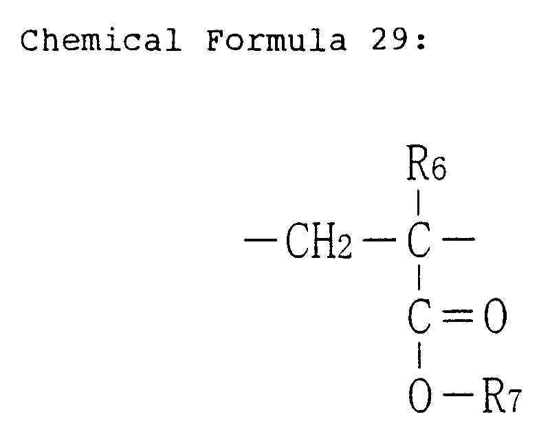 irradiating said resist film with exposing light of a wavelength of a 1 nm through 30 nm band or a 110 nm through 180 nm band for pattern exposure; andforming a resist pattern by developing said resist film after the pattern exposure.
 - The pattern formation method of Claim 15,
wherein said exposing light is F2 excimer laser, Ar2 excimer laser or soft-X rays. - A pattern formation method comprising the steps of:forming a resist film by applying, on a substrate, a pattern formation material containing a polymer including a first unit represented by Chemical Formula 30, a second unit represented by Chemical Formula 31 and a third unit represented by Chemical Formula 32, and an acid generator;
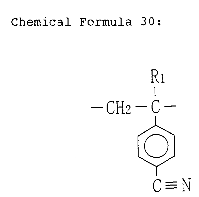
 wherein R1, R5 and R6 are the same or different and selected from the group consisting of an alkyl group, a chlorine atom and an alkyl group including a chlorine atom; and R7 is a protecting group released by an acid;
 irradiating said resist film with exposing light of a wavelength of a 1 nm through 30 nm band or a 110 nm through 180 nm band for pattern exposure; andforming a resist pattern by developing said resist film after the pattern exposure.
 - The pattern formation method of Claim 17,
wherein said exposing light is F2 excimer laser, Ar2 excimer laser or soft-X rays.
Applications Claiming Priority (2)
| Application Number | Priority Date | Filing Date | Title |
|---|---|---|---|
| JP2000071123 | 2000-03-14 | ||
| JP2000071123A JP3437138B2 (en) | 2000-03-14 | 2000-03-14 | Pattern forming material and pattern forming method |
Publications (2)
| Publication Number | Publication Date |
|---|---|
| EP1134617A2 true EP1134617A2 (en) | 2001-09-19 |
| EP1134617A3 EP1134617A3 (en) | 2001-09-26 |
Family
ID=18589749
Family Applications (1)
| Application Number | Title | Priority Date | Filing Date |
|---|---|---|---|
| EP01105830A Withdrawn EP1134617A3 (en) | 2000-03-14 | 2001-03-08 | Pattern formation material and method |
Country Status (5)
| Country | Link |
|---|---|
| US (1) | US6737213B2 (en) |
| EP (1) | EP1134617A3 (en) |
| JP (1) | JP3437138B2 (en) |
| KR (1) | KR100744330B1 (en) |
| TW (1) | TW594409B (en) |
Cited By (1)
| Publication number | Priority date | Publication date | Assignee | Title |
|---|---|---|---|---|
| CN100406481C (en) * | 2003-01-31 | 2008-07-30 | 三菱丽阳株式会社 | Polymer for resist and resist composition |
Families Citing this family (1)
| Publication number | Priority date | Publication date | Assignee | Title |
|---|---|---|---|---|
| WO2004067592A1 (en) * | 2003-01-31 | 2004-08-12 | Mitsubishi Rayon Co., Ltd. | Resist polymer and resist composition |
Family Cites Families (12)
| Publication number | Priority date | Publication date | Assignee | Title |
|---|---|---|---|---|
| US4996136A (en) | 1988-02-25 | 1991-02-26 | At&T Bell Laboratories | Radiation sensitive materials and devices made therewith |
| JPH06289617A (en) | 1993-03-30 | 1994-10-18 | Nippon Zeon Co Ltd | Resist composition |
| JP3287057B2 (en) | 1993-03-30 | 2002-05-27 | 日本ゼオン株式会社 | Resist composition |
| JPH075682A (en) | 1993-03-30 | 1995-01-10 | Nippon Zeon Co Ltd | Resist composition |
| US5688628A (en) | 1993-11-11 | 1997-11-18 | Nippon Zeon Co., Ltd. | Resist composition |
| US6004720A (en) * | 1993-12-28 | 1999-12-21 | Fujitsu Limited | Radiation sensitive material and method for forming pattern |
| US5861231A (en) * | 1996-06-11 | 1999-01-19 | Shipley Company, L.L.C. | Copolymers and photoresist compositions comprising copolymer resin binder component |
| JP3770694B2 (en) | 1997-04-30 | 2006-04-26 | 富士通株式会社 | Resist material and resist pattern forming method |
| US6284427B1 (en) | 1997-09-22 | 2001-09-04 | Clariant Finance (Bvi) Limited | Process for preparing resists |
| US6207353B1 (en) | 1997-12-10 | 2001-03-27 | International Business Machines Corporation | Resist formulation which minimizes blistering during etching |
| EP0959389B1 (en) | 1998-05-19 | 2004-03-31 | JSR Corporation | Diazodisulfone compound and radiation-sensitive resin composition |
| US6303266B1 (en) * | 1998-09-24 | 2001-10-16 | Kabushiki Kaisha Toshiba | Resin useful for resist, resist composition and pattern forming process using the same |
-
2000
- 2000-03-14 JP JP2000071123A patent/JP3437138B2/en not_active Expired - Fee Related
-
2001
- 2001-03-06 US US09/799,017 patent/US6737213B2/en not_active Expired - Lifetime
- 2001-03-07 TW TW090105306A patent/TW594409B/en not_active IP Right Cessation
- 2001-03-08 EP EP01105830A patent/EP1134617A3/en not_active Withdrawn
- 2001-03-14 KR KR1020010013068A patent/KR100744330B1/en not_active Expired - Fee Related
Cited By (1)
| Publication number | Priority date | Publication date | Assignee | Title |
|---|---|---|---|---|
| CN100406481C (en) * | 2003-01-31 | 2008-07-30 | 三菱丽阳株式会社 | Polymer for resist and resist composition |
Also Published As
| Publication number | Publication date |
|---|---|
| EP1134617A3 (en) | 2001-09-26 |
| JP3437138B2 (en) | 2003-08-18 |
| KR20010092308A (en) | 2001-10-24 |
| KR100744330B1 (en) | 2007-07-30 |
| US20010028989A1 (en) | 2001-10-11 |
| JP2001264982A (en) | 2001-09-28 |
| US6737213B2 (en) | 2004-05-18 |
| TW594409B (en) | 2004-06-21 |
Similar Documents
| Publication | Publication Date | Title |
|---|---|---|
| US6632582B2 (en) | Pattern formation material and pattern formation method | |
| US6753132B2 (en) | Pattern formation material and pattern formation method | |
| JP3415799B2 (en) | Resist material and pattern forming method | |
| EP1403711A1 (en) | PATTERN−FORMING MATERIAL AND METHOD OF FORMING PATTERN | |
| US6475706B1 (en) | Pattern formation method | |
| US6645694B2 (en) | Pattern formation material and pattern formation method | |
| US6511786B2 (en) | Pattern formation material and pattern formation method | |
| US6737213B2 (en) | Pattern formation material and method | |
| US6689536B2 (en) | Pattern formation material and pattern formation method | |
| US6576398B2 (en) | Pattern formation material and method | |
| US20030091930A1 (en) | Pattern formation material and pattern formation method | |
| US6830869B2 (en) | Pattern forming material and method of pattern formation | |
| EP1148388A1 (en) | Pattern formation material and pattern formation method | |
| US20030087184A1 (en) | Pattern formation material and pattern formation method | |
| JP3299240B2 (en) | Pattern formation method | |
| EP1335246A1 (en) | Pattern formation method | |
| JPH04149445A (en) | Positive type photosensitive composition | |
| US6537736B1 (en) | Patten formation method |
Legal Events
| Date | Code | Title | Description |
|---|---|---|---|
| PUAI | Public reference made under article 153(3) epc to a published international application that has entered the european phase |
Free format text: ORIGINAL CODE: 0009012 |
|
| PUAL | Search report despatched |
Free format text: ORIGINAL CODE: 0009013 |
|
| AK | Designated contracting states |
Kind code of ref document: A2 Designated state(s): DE FR GB NL Kind code of ref document: A2 Designated state(s): AT BE CH CY DE DK ES FI FR GB GR IE IT LI LU MC NL PT SE TR |
|
| AX | Request for extension of the european patent |
Free format text: AL;LT;LV;MK;RO;SI |
|
| AK | Designated contracting states |
Kind code of ref document: A3 Designated state(s): AT BE CH CY DE DK ES FI FR GB GR IE IT LI LU MC NL PT SE TR |
|
| AX | Request for extension of the european patent |
Free format text: AL;LT;LV;MK;RO;SI |
|
| 17P | Request for examination filed |
Effective date: 20011228 |
|
| AKX | Designation fees paid |
Free format text: DE FR GB NL |
|
| RAP1 | Party data changed (applicant data changed or rights of an application transferred) |
Owner name: PANASONIC CORPORATION |
|
| STAA | Information on the status of an ep patent application or granted ep patent |
Free format text: STATUS: THE APPLICATION HAS BEEN WITHDRAWN |
|
| 18W | Application withdrawn |
Effective date: 20090513 |