EP1134224A2 - Cyclosilane compound, and solution composition and process for forming a silicon film - Google Patents
Cyclosilane compound, and solution composition and process for forming a silicon film Download PDFInfo
- Publication number
- EP1134224A2 EP1134224A2 EP01106037A EP01106037A EP1134224A2 EP 1134224 A2 EP1134224 A2 EP 1134224A2 EP 01106037 A EP01106037 A EP 01106037A EP 01106037 A EP01106037 A EP 01106037A EP 1134224 A2 EP1134224 A2 EP 1134224A2
- Authority
- EP
- European Patent Office
- Prior art keywords
- silicon
- silylcyclopentasilane
- silicon film
- film
- cyclopentasilane
- Prior art date
- Legal status (The legal status is an assumption and is not a legal conclusion. Google has not performed a legal analysis and makes no representation as to the accuracy of the status listed.)
- Granted
Links
Images


Classifications
-
- C—CHEMISTRY; METALLURGY
- C07—ORGANIC CHEMISTRY
- C07F—ACYCLIC, CARBOCYCLIC OR HETEROCYCLIC COMPOUNDS CONTAINING ELEMENTS OTHER THAN CARBON, HYDROGEN, HALOGEN, OXYGEN, NITROGEN, SULFUR, SELENIUM OR TELLURIUM
- C07F7/00—Compounds containing elements of Groups 4 or 14 of the Periodic Table
- C07F7/02—Silicon compounds
- C07F7/21—Cyclic compounds having at least one ring containing silicon, but no carbon in the ring
-
- C—CHEMISTRY; METALLURGY
- C23—COATING METALLIC MATERIAL; COATING MATERIAL WITH METALLIC MATERIAL; CHEMICAL SURFACE TREATMENT; DIFFUSION TREATMENT OF METALLIC MATERIAL; COATING BY VACUUM EVAPORATION, BY SPUTTERING, BY ION IMPLANTATION OR BY CHEMICAL VAPOUR DEPOSITION, IN GENERAL; INHIBITING CORROSION OF METALLIC MATERIAL OR INCRUSTATION IN GENERAL
- C23C—COATING METALLIC MATERIAL; COATING MATERIAL WITH METALLIC MATERIAL; SURFACE TREATMENT OF METALLIC MATERIAL BY DIFFUSION INTO THE SURFACE, BY CHEMICAL CONVERSION OR SUBSTITUTION; COATING BY VACUUM EVAPORATION, BY SPUTTERING, BY ION IMPLANTATION OR BY CHEMICAL VAPOUR DEPOSITION, IN GENERAL
- C23C18/00—Chemical coating by decomposition of either liquid compounds or solutions of the coating forming compounds, without leaving reaction products of surface material in the coating; Contact plating
- C23C18/02—Chemical coating by decomposition of either liquid compounds or solutions of the coating forming compounds, without leaving reaction products of surface material in the coating; Contact plating by thermal decomposition
- C23C18/12—Chemical coating by decomposition of either liquid compounds or solutions of the coating forming compounds, without leaving reaction products of surface material in the coating; Contact plating by thermal decomposition characterised by the deposition of inorganic material other than metallic material
- C23C18/1204—Chemical coating by decomposition of either liquid compounds or solutions of the coating forming compounds, without leaving reaction products of surface material in the coating; Contact plating by thermal decomposition characterised by the deposition of inorganic material other than metallic material inorganic material, e.g. non-oxide and non-metallic such as sulfides, nitrides based compounds
- C23C18/1208—Oxides, e.g. ceramics
-
- C—CHEMISTRY; METALLURGY
- C07—ORGANIC CHEMISTRY
- C07F—ACYCLIC, CARBOCYCLIC OR HETEROCYCLIC COMPOUNDS CONTAINING ELEMENTS OTHER THAN CARBON, HYDROGEN, HALOGEN, OXYGEN, NITROGEN, SULFUR, SELENIUM OR TELLURIUM
- C07F7/00—Compounds containing elements of Groups 4 or 14 of the Periodic Table
- C07F7/02—Silicon compounds
- C07F7/025—Silicon compounds without C-silicon linkages
-
- C—CHEMISTRY; METALLURGY
- C23—COATING METALLIC MATERIAL; COATING MATERIAL WITH METALLIC MATERIAL; CHEMICAL SURFACE TREATMENT; DIFFUSION TREATMENT OF METALLIC MATERIAL; COATING BY VACUUM EVAPORATION, BY SPUTTERING, BY ION IMPLANTATION OR BY CHEMICAL VAPOUR DEPOSITION, IN GENERAL; INHIBITING CORROSION OF METALLIC MATERIAL OR INCRUSTATION IN GENERAL
- C23C—COATING METALLIC MATERIAL; COATING MATERIAL WITH METALLIC MATERIAL; SURFACE TREATMENT OF METALLIC MATERIAL BY DIFFUSION INTO THE SURFACE, BY CHEMICAL CONVERSION OR SUBSTITUTION; COATING BY VACUUM EVAPORATION, BY SPUTTERING, BY ION IMPLANTATION OR BY CHEMICAL VAPOUR DEPOSITION, IN GENERAL
- C23C18/00—Chemical coating by decomposition of either liquid compounds or solutions of the coating forming compounds, without leaving reaction products of surface material in the coating; Contact plating
- C23C18/02—Chemical coating by decomposition of either liquid compounds or solutions of the coating forming compounds, without leaving reaction products of surface material in the coating; Contact plating by thermal decomposition
- C23C18/12—Chemical coating by decomposition of either liquid compounds or solutions of the coating forming compounds, without leaving reaction products of surface material in the coating; Contact plating by thermal decomposition characterised by the deposition of inorganic material other than metallic material
- C23C18/1204—Chemical coating by decomposition of either liquid compounds or solutions of the coating forming compounds, without leaving reaction products of surface material in the coating; Contact plating by thermal decomposition characterised by the deposition of inorganic material other than metallic material inorganic material, e.g. non-oxide and non-metallic such as sulfides, nitrides based compounds
- C23C18/122—Inorganic polymers, e.g. silanes, polysilazanes, polysiloxanes
-
- H—ELECTRICITY
- H10—SEMICONDUCTOR DEVICES; ELECTRIC SOLID-STATE DEVICES NOT OTHERWISE PROVIDED FOR
- H10P—GENERIC PROCESSES OR APPARATUS FOR THE MANUFACTURE OR TREATMENT OF DEVICES COVERED BY CLASS H10
- H10P14/00—Formation of materials, e.g. in the shape of layers or pillars
- H10P14/20—Formation of materials, e.g. in the shape of layers or pillars of semiconductor materials
- H10P14/26—Formation of materials, e.g. in the shape of layers or pillars of semiconductor materials using liquid deposition
- H10P14/265—Formation of materials, e.g. in the shape of layers or pillars of semiconductor materials using liquid deposition using solutions
-
- H—ELECTRICITY
- H10—SEMICONDUCTOR DEVICES; ELECTRIC SOLID-STATE DEVICES NOT OTHERWISE PROVIDED FOR
- H10P—GENERIC PROCESSES OR APPARATUS FOR THE MANUFACTURE OR TREATMENT OF DEVICES COVERED BY CLASS H10
- H10P14/00—Formation of materials, e.g. in the shape of layers or pillars
- H10P14/20—Formation of materials, e.g. in the shape of layers or pillars of semiconductor materials
- H10P14/34—Deposited materials, e.g. layers
- H10P14/3402—Deposited materials, e.g. layers characterised by the chemical composition
- H10P14/3404—Deposited materials, e.g. layers characterised by the chemical composition being Group IVA materials
- H10P14/3411—Silicon, silicon germanium or germanium
-
- H—ELECTRICITY
- H10—SEMICONDUCTOR DEVICES; ELECTRIC SOLID-STATE DEVICES NOT OTHERWISE PROVIDED FOR
- H10P—GENERIC PROCESSES OR APPARATUS FOR THE MANUFACTURE OR TREATMENT OF DEVICES COVERED BY CLASS H10
- H10P14/00—Formation of materials, e.g. in the shape of layers or pillars
- H10P14/20—Formation of materials, e.g. in the shape of layers or pillars of semiconductor materials
- H10P14/34—Deposited materials, e.g. layers
- H10P14/3451—Structure
- H10P14/3452—Microstructure
- H10P14/3454—Amorphous
-
- H—ELECTRICITY
- H10—SEMICONDUCTOR DEVICES; ELECTRIC SOLID-STATE DEVICES NOT OTHERWISE PROVIDED FOR
- H10P—GENERIC PROCESSES OR APPARATUS FOR THE MANUFACTURE OR TREATMENT OF DEVICES COVERED BY CLASS H10
- H10P14/00—Formation of materials, e.g. in the shape of layers or pillars
- H10P14/20—Formation of materials, e.g. in the shape of layers or pillars of semiconductor materials
- H10P14/34—Deposited materials, e.g. layers
- H10P14/3451—Structure
- H10P14/3452—Microstructure
- H10P14/3456—Polycrystalline
-
- H—ELECTRICITY
- H10—SEMICONDUCTOR DEVICES; ELECTRIC SOLID-STATE DEVICES NOT OTHERWISE PROVIDED FOR
- H10P—GENERIC PROCESSES OR APPARATUS FOR THE MANUFACTURE OR TREATMENT OF DEVICES COVERED BY CLASS H10
- H10P14/00—Formation of materials, e.g. in the shape of layers or pillars
- H10P14/20—Formation of materials, e.g. in the shape of layers or pillars of semiconductor materials
- H10P14/38—Formation of materials, e.g. in the shape of layers or pillars of semiconductor materials characterised by treatments done after the formation of the materials
- H10P14/3802—Crystallisation or recrystallisation of non-monocrystalline semiconductor materials, e.g. regrowth
- H10P14/3808—Crystallisation or recrystallisation of non-monocrystalline semiconductor materials, e.g. regrowth using laser beams
-
- H—ELECTRICITY
- H10—SEMICONDUCTOR DEVICES; ELECTRIC SOLID-STATE DEVICES NOT OTHERWISE PROVIDED FOR
- H10P—GENERIC PROCESSES OR APPARATUS FOR THE MANUFACTURE OR TREATMENT OF DEVICES COVERED BY CLASS H10
- H10P14/00—Formation of materials, e.g. in the shape of layers or pillars
- H10P14/20—Formation of materials, e.g. in the shape of layers or pillars of semiconductor materials
- H10P14/24—Formation of materials, e.g. in the shape of layers or pillars of semiconductor materials using chemical vapour deposition [CVD]
Definitions
- the present invention relates to a novel cyclosilane compound, a solution composition for forming a silicon film and a process for forming a silicon film.
- thermal chemical vapor deposition CVD
- plasma CVD optical CVD which use monosilane gas or disilane gas
- thermal CVD J. Vac. Sci. Technology, vol. 14, pp. 1082, 1977
- plasma CVD Solid State Com., Vol. 17, pp. 1193, 1975
- thermal CVD J. Vac. Sci. Technology, vol. 14, pp. 1082, 1977
- plasma CVD Solid State Com., Vol. 17, pp. 1193, 1975
- these films have been used for the production of solar cells and liquid crystal display elements having a thin film transistor.
- JP-A 1-29661 discloses a process for forming a silicon-based thin film by liquefying a gaseous raw material on a cooled substrate, adsorbing it to the substrate and reacting it with chemically active atomic hydrogen.
- this process involves such problems that a complex apparatus is required and that it is difficult to control the thickness of a film because silicon hydride as a raw material is vaporized and cooled successively.
- JP-A 7-267621 discloses a process for coating a substrate with low-molecular weight liquid silicon hydride. This process has such problems that it is difficult to handle silicon hydride as the system is instable and that it is difficult to obtain a uniform film thickness when it is applied to a large-area substrate because silicon hydride is liquid.
- English Patent GB-2077710A reports an example of solid silicon hydride polymer but a coating film thereof cannot be formed because it is insoluble in a solvent.
- JP-A 9-237927 discloses a process for forming a silicon film by coating a substrate with a polysilane solution and thermally decomposing polysilane to liberate a silicon film in order to produce a solar cell.
- a polysilane solution and thermally decomposing polysilane to liberate a silicon film in order to produce a solar cell.
- it is difficult to obtain an amorphous or polycrystal silicon film having excellent electrical properties from a silicon compound containing carbon because thermal decomposition or optical decomposition by exposure to ultraviolet radiation causes a large amount of carbon to remain in the film as an impurity.
- JP-A 60-242612 discloses a process for forming a silicon deposition film by thermal CVD, the process comprising forming a gaseous atmosphere of a cyclic silane compound represented by the following formula and a halogen compound in a deposition chamber where a substrate is placed and providing heat energy to these compounds to form a deposition film containing silicon atoms on the substrate. (where n is 3, 4 or 5, R is H or SiH 3 ).
- the above publication enumerates compounds represented by five chemical formulas as the cyclic silane compound represented by the above formula. However, it is silent about identification data on these cyclic compounds and a production process therefor.
- Polysilanes can be generally produced from monomers having a structural unit by the following methods, for example: (a) one in which a halosilane is dehalogenated and polycondensed in the presence of an alkali metal equivalent in weight to the halogen atom (so-called Kipping method , J. Am. Chem. Soc., vol. 110, pp. 2342, (1988), Macromolecules, vol. 23, pp. 3423, (1990)); (b) one in which a halosilane is dehalogenated and polycondensed by electrode reduction (J. Chem, Soc., Chem, Commun., pp. 1161, (1990), J. Chem. Soc., Chem. Commun., pp.
- cyclosilane halide compounds may be synthesized by known methods (for example, Mh. Chem. vol. 106, pp. 503, (1975)), (Z. Anorg. Allg. Chem. vol. 621, pp. 1517, (1995)), (J. Chem. Soc., Chem. Commun., pp. 777, (1984)).
- a polysilane is generally synthesized by a polycondensation reaction but the step of purifying a synthesized polymer is needed as a salt is by-produced by polycondensation. It has recently been disclosed in "Macromolecules, vol. 27, pp.
- poly(phenylnanomethylpentasilanylene) 2 is synthesized by the anionic ring-opening polymerization of phenylnanomethylcyclopentasilane 1.
- the ring-opening polyaddition reaction of this cyclic monomer by-produces nothing unlike the above polycondensation reaction and is excellent as a means of synthesizing a high-purity polysilane.
- This ring-opening addition polymerization is particularly preferred in application fields which require high purity such as electronic materials.
- the above monomer has the carbon atom of a methyl group (Me) or phenyl group (Ph) bonded to a silicon atom, even when the above polysilane is thermally decomposed, polycarbosilane containing a carbon atom is formed, while silicon for semiconductors cannot be obtained.
- silylcyclopentasilane represented by the following formula (A):
- a solution composition for forming a silicon film which contains cyclopentasilane represented by the following formula (B) and silylcyclopentasilane represented by the above formula (A):
- spiro[4.4]nonasilane represented by the following formula (C) and having the function of radically ring-opening polymerizing cyclopentasilane like the silylcyclopentasilane of the present invention:
- the inventors of the present invention have succeeded in converting all the phenyl group substituents of the skeleton of cyclohexasilane into hydrogen atoms and the skeleton of cyclohexasilane into the skeleton of silylcyclopentasilane at the same time as follows.
- To convert the phenyl groups bonded to the silicon of dodecaphenylcyclohexasilane into hydrogen atoms they carry out a treatment with an aluminum chloride catalyst as a Lewis acid to convert the skeleton, hydrogenation by introducing hydrogen chloride gas, and reduction with lithium aluminum hydride.
- silylcyclopentasilane consisting of silicon atoms and hydrogen atoms of the present invention.
- silylcyclopentasilane consisting of silicon atoms and hydrogen atoms of the present invention has the chemical property of converting cyclopentasilane consisting of silicon atoms and hydrogen atoms into a solvent-soluble polysilane by radical ring-opening addition polymerization.
- the obtained polysilane solution has excellent coatability and is capable of forming on a substrate a satisfactory polysilane coating film which can be converted into a metallic silicon film by a dehydrogenation reaction caused by thermal decomposition or optical decomposition.
- the silylcyclopentasilane of the present invention can be used as a radical polymerization initiator for cyclopentasilane. That is, even when only cyclopentasilane is dissolved in a hydrocarbon-based solvent such as toluene and this solution is heated at around the boiling point of the solvent, a polymerization reaction does not proceed. Meanwhile, when cyclopentasilane and a small amount, for example, 1 wt% of silylcyclopentasilane are dissolved in a hydrocarbon-based solvent such as toluene, the polymerization reaction of cyclopentasilane proceeds smoothly.
- silyl group (SiH 3 ) of silylcyclopentasilane is cleaved into radicals and the formed radicals initiate the polymerization of cyclopentasilane.
- the solution composition for forming a silicon film of the present invention contains silylcyclopentasilane and cyclopentasilane.
- the solution composition of the present intention can be prepared by dissolving these compounds in an appropriate solvent.
- Any solvent is acceptable if it dissolves cyclopentasilane and silylcyclopentasilane and does not react with a solvent.
- Preferred examples of the solvent include hydrocarbon-based solvents such as n-heptane, n-octane, decane, toluene, xylene, cymene, durene, indene, dipentene, tetrahydronaphthalene, decahydronaphthalene and cyclohexylbenzene; ether-based solvents such as ethylene glycol dimethyl ether, ethylene glycol diethyl ether, ethylene glycol methyl ethyl ether, diethylene glycol dimethyl ether, diethylene glycol diethyl ether, diethylene glycol methyl ethyl ether and p-dioxane; and aprotic solvents such as
- hydrocarbon-based solvents and ether-based solvents are more preferred from the viewpoints of the solubility of a cyclic silicon compound and the stability of the solution, ether-based solvents are much more preferred, and hydrocarbon-based solvents are particularly preferred. These solvents may be used alone or in admixture of two or more.
- the solution composition of the present invention can be prepared by making effective use of silylcyclopentasilane by-produced by the synthesis of cyclopentasilane. That is, diphenyldichlorosilane is cyclized by magnesium or metallic lithium contained in tetrahydrofuran to form decaphenylcyclopentasilane and dodecaphenylcyclohexasilane, and a mixture of these is treated in toluene with aluminum chloride, hydrogen chloride gas and then a combination of lithium aluminum hydride and silica gel to form cyclopentasilane from decaphenylcyclopentasilane and skeleton converted silylcyclopentasilane from dodecaphenylcyclohexasilane.
- a solution of a mixture of silylcyclopentasilane and cyclopentasilane can be used as the solution composition of the present invention.
- the solid content of the solution composition of the present invention is preferably 0.01 to 30 wt%, more preferably 0.1 to 20 wt%, particularly preferably 1 to 10 wt% though its appropriate range differs according to the thickness of a silicon film to be formed.
- the amount of silylcyclopentasilane is preferably 0.01 to 30 parts by weight, more preferably 0.5 to 20 parts by weight based on 100 parts by weight of cyclopentasilane.
- the solution composition of the present invention is prepared as described above, for example.
- this solution composition is applied to a substrate to form a coating film.
- the material, shape and the like of the substrate are not particularly limited but a material which can withstand the heat treatment of the subsequent step is preferred.
- the substrate on which the coating film is formed is preferably flat.
- the substrate is made from glass, metal, plastic or ceramic.
- the glass is selected from quartz glass, borosilicate glass, soda glass and lead glass
- the metal is selected from gold, silver, copper, nickel, aluminum, iron and stainless steel
- the plastic is selected from polyimide and polyether sulfone.
- the shape of the material is not particularly limited and may be plate-like or film-like.
- the solution composition can be filtered with a membrane filter made from Teflon or regenerated cellulose to remove solid foreign matter.
- the coating method is not particularly limited and may be carried on by spin coating, dip coating, curtain coating, roll coating, spray coating or ink jet coating. Coating can be carried out one time or plural times.
- the preferred thickness of the coating film which changes according to the solid content is preferably 0.01 to 100 ⁇ m, more preferably 0.1 to 10 ⁇ m after the solvent is removed.
- the coating film is heated.
- the solvent contained in the solution composition is volatilized and the silicon compound contained in the coating film is decomposed to form a silicon film.
- the formed silicon film has uniform thickness and a mirror surface thanks to silylcyclopentasilane contained in the coating film heated in the step (3). This is because a silicon film having nonuniform thickness is often obtained or a partially broken silicon film is obtained in some cases from a coating film containing no silylcyclopentasilane.
- the heating temperature is preferably 300°C or more, more preferably 400 to 500°C.
- the heating time is approximately 30 seconds to 30 minutes.
- the heating atmosphere is preferably an inert atmosphere such as nitrogen, helium or argon atmosphere. It may contain a reducing gas such as hydrogen as required.
- the solvent is first volatilized by heating, the radical ring-opening reaction of cyclopentasilane occurs at the same time or after volatilization, part of cyclopentasilane is converted into an oligomer, hydrogen is formed by the thermal decomposition of this oligomer and cyclopentasilane, and a silicon film is formed at the same time.
- the contained silylcyclopentasilane forms a silyl radical and cyclopentasilanyl radical even when it is deprived of the silyl group.
- the coating film may be irradiated with ultraviolet radiation before heating as required.
- the ultraviolet radiation having dosage of 0.1 to 100 J/cm 2 at 365 nm suffices.
- the light source of ultraviolet radiation may be a low-pressure or high-pressure mercury lamp, heavy hydrogen lamp, argon, krypton or xenon rare gas discharge lamp, YAG laser, argon laser, carbon acid gas laser, or XeF, XeCl, XeBr, KrF, KrCl, ArF or ArCl excimer laser. These light sources generally have an output of 10 to 5,000 W but an output of 100 to 1,000 W suffices.
- a silicon film particularly an amorphous silicon film can be advantageously formed on the substrate.
- the thickness of the silicon film can be 0.001 to 10 ⁇ m.
- the solution composition of the present invention may contain a trace amount of a fluorine-based, silicone-based or nonionic surface tension controlling material as required unless it impairs the object of the present invention.
- This nonionic surface tension controlling material improves the wettability of the solution for an object to be coated, the leveling properties of a coating film and prevents the formation of bumps on the coating film.
- the nonionic surfactant is a fluorine-based surfactant having a fluoroalkyl group or perfluoroalkyl group, or polyetheralkyl-based surfactant having an oxyalkyl group.
- fluorine-based surfactant examples include C 9 F 19 CONHC 12 H 25 , C 8 F 17 SO 2 NH-(C 3 H 4 O) 6 H, C 9 F 17 O(Pulronic L-35)C 9 F 17 , C 9 F 17 O(Pulronic P-84)C 9 F 17 and C 9 F 7 O(Tetronic-704)(C 9 F 17 ) 2
- Pulronic L-35 manufactured by Asahi Denka Kogyo K.K., polyoxypropylene-polyoxyethylene block copolymer having an average molecular weight of 1,900
- Pulronic P-84 manufactured by Asahi Denka Kogyo K.K., polyoxypropylene-polyoxyethylene block copolymer having an average molecular weight of 4,200
- Tetronic-704 manufactured by Asahi Denka Kogyo K.K., N,N,N ,N - tetrakis (polyoxypropylene-polyoxyethylene block copo
- F Top EF301, EF303 and EF352 of Shin Akita Kasei Co., Ltd.
- Megafac F171 and F173 of Dainippon Ink and Chemicals, Inc.
- Asahi Guard AG710 of Asahi Glass Co., Ltd.
- Florade FC-170C, FC430 and FC431 Florade FC-170C, FC430 and FC431 (Sumitomo 3M, Ltd.)
- Surflon S-382, SC101, SC102, SC103, SC104, SC105 and SC106 of Asahi Glass Co., Ltd.
- BM-1000 and 1100 of B.M-Chemie Co., Ltd.
- Schsego-Fluor of Schwegmann Co., Ltd.
- polyetheralkyl-based surfactant examples include polyoxyethylenealkyl ethers, polyoxyethyleneallyl ethers, polyoxyethylenealkyl phenol ethers, polyoxyethylene fatty acid esters, sorbitan fatty acid esters, polyoxyethylene sorbitan fatty acid esters and oxyethylene oxypropylene block polymers.
- Emulgen 105, 430, 810 and 920 Commercially available products of the polyetheralkyl-based surfactant include Emulgen 105, 430, 810 and 920, Leodor SP-40S and TW-L120, Emanol 3199 and 4110, Excel P-40S, Bridge 30, 52, 72 and.92, Arassel 20, Emasol 320, Tween 20 and 60, and Merge 45 (of Kao Corporation) and Noniball 55 (of Sanyo Chemical Industries, Ltd.).
- Nonionic surfactants other than the above include polyoxyethylene fatty acid esters, polyoxyethylene sorbitan fatty acid esters and polyalkylene oxide block copolymers and commercially available products thereof include Chemistat 2500 (of Sanyo Chemical Industries, Ltd.), SN-EX9228 (of Sun Nopco Co., Ltd.) and Nonale 530 (of Toho Chemical Ind., Co., Ltd.).
- the amorphous silicon film formed by the present invention is used in various electronic devices such as solar cells, photosensors, thin film transistors, photosensitive drums and protective films.
- spiro[4.4]nonasilane which has the function of radically ring-opening polymerizing cyclopentasilane like the silylcyclopentasilane of the present invention.
- the spiro[4.4]nonasilane of the present invention can be synthesized by known methods in which a phenyl group bonded to the silicon atom of hexadecaphenylspiro[4.4]nonasilane is converted into a chlorine atom and then converted into a hydrogen atom (for example, Mh. Chem. vol. 106, pp. 503, (1975)), (Z. Anorg. Allg. Chem. vol. 621, pp. 1517, (1995)), (J. Chem. Soc., Chem. Commun., 777, (1984)).
- hexadecaphenylspiro[4.4]nonasilane is chlorinated by introducing hydrogen chloride gas in the presence of a Lewis acid catalyst such as aluminum chloride and then hydrogenated with lithium aluminum hydride to convert all the phenyl substituents of hexadecaphenylspiro[4.4]nonasilane into hydrogen atoms to produce spiro[4.4]nonasilane consisting of silicon atoms and hydrogen atoms.
- a Lewis acid catalyst such as aluminum chloride
- the chlorination reaction can be carried out at a temperature of 0 to 80° C for 1 to 12 hours.
- the Lewis acid catalyst may be used in an amount of 0.1 to 20 wt% based on hexadecaphenylspiro[4.4]nonasilane.
- An organic solvent such as toluene is used as the reaction solvent.
- the reduction reaction is carried out at a temperature of 0 to 50°C for 1 to 24 hours.
- the hexadecaphenylspiro[4.4]nonasilane as a raw material is obtained by the dehalogenation and condensation of diphenyldichlorosilane and tetrachlorosilane in the presence of metallic lithium.
- the silylcyclopentasilane of the present invention may be used as a radical polymerization initiator for cyclopentasilane and also a radical initiator for a vinyl monomer.
- a vinyl polymer having a silicon atom at the terminal of a polymer molecule is obtained, thereby making it possible to derive a block or random copolymer of the vinyl polymer and a silicon-based polymer.
- vinyl monomer examples include aromatic vinyl compounds such as styrene, ⁇ -methylstyrene, o-vinyltoluene, m-vinyltoluene, p-vinyltoluene, p-chlorostyene, o-methoxystyrene, m-methoxystyrene and p-methoxystyrene; acrylates and methacrylates such as methyl acrylate, methyl methacrylate, ethyl acrylate, ethyl methacrylate, n-propyl acrylate, n-propyl methacrylate, i-propyl acrylate, i-propyl methacrylate, n-butyl acrylate, n-butyl methacrylate, i-butyl acrylate, i-butyl methacrylate, sec-butyl acrylate, sec-butyl methacrylate,
- this crude product was recrystallized with ethyl acetate to obtain 216 g of dodecaphenylcyclohexasilane.
- the structure of this product was confirmed by TOF-MS, NMR and IR. Thereafter, 100 g of this dodecaphenylcyclohexasilane and 1,000 ml of toluene were charged into a 2-liter flask, 50 g of aluminum chloride was added and stirred at room temperature in an argon gas atmosphere for 5 hours and then hydrogen chloride gas was introduced until the phenyl group disappeared.
- the product obtained from this reaction was found to be dodecachlorocyclohexasilane by its 29 Si-NMR and IR spectra.
- reaction mixture was gradually added to a solution of 42 g of lithium aluminum hydride suspended in 500 ml of diethyl ether and stirred at room temperature for 12 hours. This reaction mixture was filtered to obtain an achromatic and transparent silylcyclopentasilane solution.
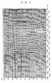
- silylcyclopentasilane was oily at room temperature and its infrared absorption spectrum is shown in Fig. 1.
- This silylcyclopentasilane consists of silicon atoms and hydrogen atoms, its infrared spectrum is relatively simple, a sharp peak attributed to the stretching vibration of a silicon-hydrogen bond is observed at 2,125 cm -1 and peaks attributed to the stretching vibration of a silicon-silicon bond are observed at 985 cm -1 and 863 cm -1 .
- Fig. 2 shows the mass spectrum of the silylcyclopentasilane. Since a molecular ion peak is observed at an m/e of 180, the molecular weight of the substance is 180.
- a strong peak detected at an m/e of 148 is attributed to a fragment formed by the elimination of one monosilane (SiH 4 ) from the molecule of silylcyclopentasilane and a peak at an m/e of 116 is attributed to a fragment formed by the elimination of two monosilanes from the molecule of silylcyclopentasilane.
- silylcyclopentasilane can be easily dissolved in an ordinary organic solvent such as a hydrocarbon solvent exemplified by benzene, toluene, xylene, hexane, cyclohexane, indane and decahydronaphthalene, ether-based solvent exemplified by diethyl ether, tetrahydrofuran, monoglyme and diglyme, or ketone-based solvent exemplified by acetone, methyl ethyl ketone, methyl isobutyl ketone or methyl amyl ketone in any ratio.
- an ordinary organic solvent such as a hydrocarbon solvent exemplified by benzene, toluene, xylene, hexane, cyclohexane, indane and decahydronaphthalene
- ether-based solvent exemplified by diethyl ether, tetrahydrofuran, mono
- Silylcyclopentasilane is an achromatic and transparent oily substance at room temperature as described above and extremely stable in an inert atmosphere such as argon or nitrogen. However, when it is left in the air, it is gradually oxidized and readily converted into a siloxane structure.
- silylcyclopentasilane is heated at 300° C or more in an inert atmosphere, a dehydrogenation reaction occurs to convert it into amorphous metallic silicon. Further, this silylcyclopentasilane generates a radical by heating at approximately 100°C to radically ring-opening polymerize the above cyclopentasilane to convert it into a solvent-soluble polysilane. Further, it can polymerize a radical polymerizable monomer such as a vinyl compound exemplified by a general acrylic compound.
- the gas chromatography of silylcyclopentasilane and cyclopentasilane is obtained by using Chromosorb W (60 to 80 mesh) as a carrier, silicone OV-17 (5 %) as a liquid phase and helium gas at 120°C (see Fig. 5 and Fig. 6).
- triphenylsilylphenyldichlorosilane 50 g was added and reacted while this dark brown dianion solution was stirred at room temperature.
- the reaction mixture was poured into 2 liters of iced water to precipitate the product.
- the obtained product was separated by filtration, washed in water and then cyclohexane and dried under reduced pressure to obtain 108 g of triphenylsilylnonaphenylcyclopentasilane.
- triphenylsilylnonaphenylcyclopentasilane was dissolved in 500 ml of toluene and 5 g of anhydrous alminum chloride was added to react hydrogen chloride gas with triphenylsilylnonaphenylcyclopentasilane until a phenyl group disappeared. Thereafter, this reaction product solution was added to a solution containing 20 g of lithium aluminum hydride suspended in 100 ml of diethyl ether and stirred at room temperature for 12 hours. The reaction mixture was treated with a silica gel and concentrated to obtain an achromatic and transparent oily substance. The IR and MS spectra of this substance was identified with those of the product of above Example 1.
- Fig. 7 shows the ESCA spectrum of the silicon film.
- spiro[4.4]nonasilane There is also disclosed spiro[4.4]nonasilane.
Landscapes
- Chemical & Material Sciences (AREA)
- Organic Chemistry (AREA)
- Engineering & Computer Science (AREA)
- Materials Engineering (AREA)
- Physics & Mathematics (AREA)
- Thermal Sciences (AREA)
- General Chemical & Material Sciences (AREA)
- Chemical Kinetics & Catalysis (AREA)
- Inorganic Chemistry (AREA)
- Mechanical Engineering (AREA)
- Metallurgy (AREA)
- Ceramic Engineering (AREA)
- Silicon Compounds (AREA)
- Silicon Polymers (AREA)
- Organic Low-Molecular-Weight Compounds And Preparation Thereof (AREA)
- Liquid Deposition Of Substances Of Which Semiconductor Devices Are Composed (AREA)
Abstract
Description

The above publication enumerates compounds represented by five chemical formulas as the cyclic silane compound represented by the above formula. However, it is silent about identification data on these cyclic compounds and a production process therefor. Polysilanes can be generally produced from monomers having a structural unit by the following methods, for example: (a) one in which a halosilane is dehalogenated and polycondensed in the presence of an alkali metal equivalent in weight to the halogen atom (so-called Kipping method , J. Am. Chem. Soc., vol. 110, pp. 2342, (1988), Macromolecules, vol. 23, pp. 3423, (1990)); (b) one in which a halosilane is dehalogenated and polycondensed by electrode reduction (J. Chem, Soc., Chem, Commun., pp. 1161, (1990), J. Chem. Soc., Chem. Commun., pp. 896, (1992); (c) one in which a hydrosilane is dehydrogenated and polycondensed in the presence of a metal catalyst (JP-A 4-334551); (d) one in which a disilane crosslinked by biphenyl is anionically polymerized (Macromolecules, vol. 23, pp. 4494, (1990)); and (e) one in which a cyclic silicon compound substituted by a phenyl group or alkyl group is synthesized by one of the above methods and induced into a hydro-substituted material or halogen-substituted material by a known method (for example, Z. Anorg. Allg. Chem., vol. 459, pp. 123, (1979)). These cyclosilane halide compounds may be synthesized by known methods (for example, Mh. Chem. vol. 106, pp. 503, (1975)), (Z. Anorg. Allg. Chem. vol. 621, pp. 1517, (1995)), (J. Chem. Soc., Chem. Commun., pp. 777, (1984)). As described above, a polysilane is generally synthesized by a polycondensation reaction but the step of purifying a synthesized polymer is needed as a salt is by-produced by polycondensation. It has recently been disclosed in "Macromolecules, vol. 27, pp. 2360, (1994))" that poly(phenylnanomethylpentasilanylene) 2 is synthesized by the anionic ring-opening polymerization of


Claims (4)
- Silylcyclopentasilane represented by the following formula (A):

- A solution composition for forming a silicon film which contains cyclopentasilane represented by the following formula (B):and silylcyclopentasilane represented by the above formula (A).

- A process for forming a silicon film on the surface of a substrate comprising the steps of:(1) preparing the solution composition for forming a silicon film of claim 2;(2) coating the surface of the substrate with this solution composition to form a coating film; and(3) heating this coating film to form a silicon film.
- Spiro[4.4]nonasilane represented by the following formula (C):

Applications Claiming Priority (6)
| Application Number | Priority Date | Filing Date | Title |
|---|---|---|---|
| JP2000069313A JP4518222B2 (en) | 2000-03-13 | 2000-03-13 | Silylcyclopentasilane and its uses |
| JP2000069313 | 2000-03-13 | ||
| JP2000069314 | 2000-03-13 | ||
| JP2000069314A JP3424232B2 (en) | 2000-03-13 | 2000-03-13 | Method of forming silicon film |
| JP2000164102 | 2000-06-01 | ||
| JP2000164102A JP4748288B2 (en) | 2000-06-01 | 2000-06-01 | Composition containing spiro [4.4] nonasilane |
Publications (3)
| Publication Number | Publication Date |
|---|---|
| EP1134224A2 true EP1134224A2 (en) | 2001-09-19 |
| EP1134224A3 EP1134224A3 (en) | 2003-01-15 |
| EP1134224B1 EP1134224B1 (en) | 2007-05-30 |
Family
ID=27342650
Family Applications (1)
| Application Number | Title | Priority Date | Filing Date |
|---|---|---|---|
| EP01106037A Expired - Lifetime EP1134224B1 (en) | 2000-03-13 | 2001-03-12 | Cyclosilane compound, and solution composition and process for forming a silicon film |
Country Status (5)
| Country | Link |
|---|---|
| US (1) | US6503570B2 (en) |
| EP (1) | EP1134224B1 (en) |
| KR (1) | KR100562815B1 (en) |
| DE (1) | DE60128611T2 (en) |
| TW (1) | TWI281921B (en) |
Cited By (5)
| Publication number | Priority date | Publication date | Assignee | Title |
|---|---|---|---|---|
| DE102009053806A1 (en) | 2009-11-18 | 2011-05-19 | Evonik Degussa Gmbh | Process for producing silicon layers |
| WO2011104147A1 (en) | 2010-02-26 | 2011-09-01 | Evonik Degussa Gmbh | Method for oligomerizing hydridosilanes, the oligomers that can be produced by means of the method, and the use thereof |
| DE102011006307A1 (en) | 2011-03-29 | 2012-10-04 | Evonik Degussa Gmbh | Method for producing amorphous semiconductor layers |
| US9346966B2 (en) | 2010-04-06 | 2016-05-24 | Ndsu Research Foundation | Liquid silane-based compositions and methods for producing silicon-based materials |
| EP2145350B1 (en) * | 2007-05-04 | 2020-04-15 | Thin Film Electronics ASA | Print processing for patterned conductor, semiconductor and dielectric materials |
Families Citing this family (30)
| Publication number | Priority date | Publication date | Assignee | Title |
|---|---|---|---|---|
| US6767775B1 (en) * | 1999-03-30 | 2004-07-27 | Seiko Epson Corporation | Method of manufacturing thin-film transistor |
| EP1284306B1 (en) * | 2001-08-14 | 2011-08-03 | JSR Corporation | Silane composition, silicon film forming method and solar cell production method |
| CN100423197C (en) * | 2002-08-23 | 2008-10-01 | Jsr株式会社 | Composition for forming silicon film and method for forming silicon film |
| GB0225202D0 (en) * | 2002-10-30 | 2002-12-11 | Hewlett Packard Co | Electronic components |
| US7078276B1 (en) * | 2003-01-08 | 2006-07-18 | Kovio, Inc. | Nanoparticles and method for making the same |
| US7879696B2 (en) * | 2003-07-08 | 2011-02-01 | Kovio, Inc. | Compositions and methods for forming a semiconducting and/or silicon-containing film, and structures formed therefrom |
| US7815864B2 (en) * | 2003-11-20 | 2010-10-19 | Sigma-Aldrich Co. | Polysilazane thermosetting polymers for use in chromatographic systems and applications |
| US7498015B1 (en) | 2004-02-27 | 2009-03-03 | Kovio, Inc. | Method of making silane compositions |
| US7757631B2 (en) * | 2004-05-26 | 2010-07-20 | Hewlett-Packard Development Company, L.P. | Apparatus for forming a circuit |
| US7485691B1 (en) * | 2004-10-08 | 2009-02-03 | Kovio, Inc | Polysilane compositions, methods for their synthesis and films formed therefrom |
| US7709307B2 (en) * | 2006-08-24 | 2010-05-04 | Kovio, Inc. | Printed non-volatile memory |
| WO2008045327A2 (en) * | 2006-10-06 | 2008-04-17 | Kovio, Inc. | Silicon polymers, methods of polymerizing silicon compounds, and methods of forming thin films from such silicon polymers |
| US20090053507A1 (en) * | 2007-08-17 | 2009-02-26 | Ndsu Research Foundation | Convergent-divergent-convergent nozzle focusing of aerosol particles for micron-scale direct writing |
| CA2701412C (en) * | 2007-10-01 | 2017-06-20 | Kovio, Inc. | Profile engineered thin film devices and structures |
| US9564629B2 (en) * | 2008-01-02 | 2017-02-07 | Nanotek Instruments, Inc. | Hybrid nano-filament anode compositions for lithium ion batteries |
| US20090283766A1 (en) * | 2008-05-19 | 2009-11-19 | Silexos, Inc. | Methods for increasing film thickness during the deposition of silicon films using liquid silane materials |
| WO2009148878A2 (en) * | 2008-05-29 | 2009-12-10 | Ndsu Research Foundation | Method of forming functionalized silanes |
| CN102089358A (en) * | 2008-07-11 | 2011-06-08 | 独立行政法人科学技术振兴机构 | The production method of polysilane |
| US9336925B1 (en) | 2008-11-26 | 2016-05-10 | Thin Film Electronics Asa | Siloxanes, doped siloxanes, methods for their synthesis, compositions containing the same, and films formed therefrom |
| KR101175405B1 (en) * | 2009-09-03 | 2012-08-20 | 신동윤 | Method for preparing polysilanes, polysilanes prepared thereby, dehydrogenation catalyst used for the method, method for manufacturing amorphous silicon thin film using the polysilanes |
| DE102009053805A1 (en) * | 2009-11-18 | 2011-05-26 | Evonik Degussa Gmbh | Silicon layers of polymer-modified liquid silane formulations |
| US8624049B2 (en) * | 2010-01-18 | 2014-01-07 | Kovio, Inc. | Dopant group-substituted semiconductor precursor compounds, compositions containing the same, and methods of making such compounds and compositions |
| US8975429B2 (en) | 2010-01-28 | 2015-03-10 | Ndsu Research Foundation | Method of producing cyclohexasilane compounds |
| WO2011116223A1 (en) * | 2010-03-18 | 2011-09-22 | Board Of Regents The University Of Texas System | Silicon-containing block co-polymers, methods for synthesis and use |
| JP5442572B2 (en) | 2010-09-28 | 2014-03-12 | 株式会社日立ハイテクサイエンス | Charged particle beam apparatus, thin film manufacturing method, defect correcting method, and device manufacturing method |
| JP5902572B2 (en) | 2012-07-04 | 2016-04-13 | 株式会社日本触媒 | Method for producing halogenated cyclic silane compound having silicon-halogen bond or salt thereof |
| DE102012221669A1 (en) * | 2012-11-27 | 2014-05-28 | Evonik Industries Ag | Process for producing carbon-containing hydridosilanes |
| KR20170035929A (en) | 2014-07-16 | 2017-03-31 | 씬 필름 일렉트로닉스 에이에스에이 | High-molecular-weight polysilane and method for producing the same |
| JP6800879B2 (en) * | 2015-03-30 | 2020-12-16 | メルク パテント ゲーエムベーハー | Formulations of organic functional materials containing siloxane solvents |
| JP6534959B2 (en) * | 2016-04-21 | 2019-06-26 | 信越化学工業株式会社 | Method of forming organic film and method of manufacturing substrate for semiconductor device |
Family Cites Families (17)
| Publication number | Priority date | Publication date | Assignee | Title |
|---|---|---|---|---|
| GB2077710B (en) | 1980-06-11 | 1983-10-12 | Nat Res Dev | Synthesising a polysilane |
| JPS6026664A (en) * | 1983-07-22 | 1985-02-09 | Canon Inc | Formation of deposited amorphous silicon film |
| US4683145A (en) * | 1984-04-16 | 1987-07-28 | Canon Kabushiki Kaisha | Method for forming deposited film |
| JPH0712024B2 (en) | 1984-05-16 | 1995-02-08 | キヤノン株式会社 | Method of forming deposited film |
| US4657777A (en) * | 1984-12-17 | 1987-04-14 | Canon Kabushiki Kaisha | Formation of deposited film |
| US4820788A (en) * | 1986-10-31 | 1989-04-11 | John M. Zeigler | Poly(silyl silane)homo and copolymers |
| JPS6429661A (en) | 1987-07-24 | 1989-01-31 | Mikuni Kogyo Kk | Air-fuel mixture feeder |
| JPH04334551A (en) | 1991-05-10 | 1992-11-20 | Tonen Corp | Polymerization catalyst of hydrosilane |
| JP3517934B2 (en) | 1994-03-24 | 2004-04-12 | 昭和電工株式会社 | Method of forming silicon film |
| JPH09237927A (en) | 1995-12-26 | 1997-09-09 | Toshiba Corp | Semiconductor thin film forming method and solar cell manufacturing method |
| JP3408399B2 (en) * | 1997-05-23 | 2003-05-19 | シャープ株式会社 | Method of forming silicon film |
| JP2000007317A (en) * | 1998-06-19 | 2000-01-11 | Sharp Corp | Method of forming silicon film |
| DE60036449T2 (en) * | 1999-03-30 | 2008-06-19 | Seiko Epson Corp. | METHOD FOR HOLDING A THIN-FILTER EFFECT TRANSISTOR |
| DE60039744D1 (en) * | 1999-03-30 | 2008-09-18 | Seiko Epson Corp | Process for the preparation of a silicon layer |
| CN1223011C (en) * | 1999-03-30 | 2005-10-12 | 精工爱普生株式会社 | Manufacturing method of solar cell |
| CN1297578A (en) * | 1999-03-30 | 2001-05-30 | 捷时雅株式会社 | Method for forming silicon oxide film |
| WO2000059014A1 (en) * | 1999-03-30 | 2000-10-05 | Seiko Epson Corporation | Method for forming a silicon film and ink composition for ink jet |
-
2001
- 2001-03-12 DE DE60128611T patent/DE60128611T2/en not_active Expired - Lifetime
- 2001-03-12 KR KR1020010012516A patent/KR100562815B1/en not_active Expired - Fee Related
- 2001-03-12 TW TW090105731A patent/TWI281921B/en not_active IP Right Cessation
- 2001-03-12 US US09/802,918 patent/US6503570B2/en not_active Expired - Fee Related
- 2001-03-12 EP EP01106037A patent/EP1134224B1/en not_active Expired - Lifetime
Cited By (8)
| Publication number | Priority date | Publication date | Assignee | Title |
|---|---|---|---|---|
| EP2145350B1 (en) * | 2007-05-04 | 2020-04-15 | Thin Film Electronics ASA | Print processing for patterned conductor, semiconductor and dielectric materials |
| DE102009053806A1 (en) | 2009-11-18 | 2011-05-19 | Evonik Degussa Gmbh | Process for producing silicon layers |
| WO2011061106A2 (en) | 2009-11-18 | 2011-05-26 | Evonik Degussa Gmbh | Method for producing silicon layers |
| WO2011104147A1 (en) | 2010-02-26 | 2011-09-01 | Evonik Degussa Gmbh | Method for oligomerizing hydridosilanes, the oligomers that can be produced by means of the method, and the use thereof |
| DE102010002405A1 (en) | 2010-02-26 | 2011-09-01 | Evonik Degussa Gmbh | A process for the oligomerization of hydridosilanes, the process of preparing oligomerizates and their use |
| US9346966B2 (en) | 2010-04-06 | 2016-05-24 | Ndsu Research Foundation | Liquid silane-based compositions and methods for producing silicon-based materials |
| DE102011006307A1 (en) | 2011-03-29 | 2012-10-04 | Evonik Degussa Gmbh | Method for producing amorphous semiconductor layers |
| WO2012130620A1 (en) | 2011-03-29 | 2012-10-04 | Evonik Degussa Gmbh | Method for producing amorphous semiconductor layers |
Also Published As
| Publication number | Publication date |
|---|---|
| DE60128611D1 (en) | 2007-07-12 |
| EP1134224A3 (en) | 2003-01-15 |
| DE60128611T2 (en) | 2008-01-31 |
| EP1134224B1 (en) | 2007-05-30 |
| TWI281921B (en) | 2007-06-01 |
| US6503570B2 (en) | 2003-01-07 |
| KR20010091967A (en) | 2001-10-23 |
| KR100562815B1 (en) | 2006-03-23 |
| US20010021760A1 (en) | 2001-09-13 |
Similar Documents
| Publication | Publication Date | Title |
|---|---|---|
| US6503570B2 (en) | Cyclosilane compound, and solution composition and process for forming a silicon film | |
| US7173180B2 (en) | Silane composition, silicon film forming method and solar cell production method | |
| US6527847B1 (en) | Coating composition | |
| US6517911B1 (en) | Process for the formation of silicon oxide films | |
| EP1715509B1 (en) | Method of forming silicon films | |
| JPWO2000058409A1 (en) | Coating Composition | |
| JP2003171556A (en) | Method for forming silicon film and composition therefor | |
| JP2003055556A (en) | Method for forming silicon film or silicon oxide film and composition therefor | |
| JP2001262058A (en) | Composition for forming silicon film and method for forming silicon film | |
| JP4518222B2 (en) | Silylcyclopentasilane and its uses | |
| JP4419357B2 (en) | Silane composition and method for producing solar cell using the same | |
| JP2002246384A (en) | Method for forming silicon oxide film and composition for formation | |
| JP4748288B2 (en) | Composition containing spiro [4.4] nonasilane | |
| JP4548567B2 (en) | Method for forming silicon oxide film | |
| JP2001089572A (en) | Phosphorus-modified silicon polymer, method for producing the same, composition containing the same, and method for producing phosphorus-modified silicon | |
| JP2001058996A (en) | Silicon compound having norbornyl group, coating composition and method for producing silicon film | |
| JP2008143782A (en) | Method for manufacturing solar cell | |
| JP2001011184A (en) | Silicon polymer and method for producing the same | |
| JPWO2000059022A1 (en) | Silicon oxide film formation method | |
| US20170313591A1 (en) | Polymerization Inhibitor for Silane |
Legal Events
| Date | Code | Title | Description |
|---|---|---|---|
| PUAI | Public reference made under article 153(3) epc to a published international application that has entered the european phase |
Free format text: ORIGINAL CODE: 0009012 |
|
| AK | Designated contracting states |
Kind code of ref document: A2 Designated state(s): AT BE CH CY DE DK ES FI FR GB GR IE IT LI LU MC NL PT SE TR |
|
| AX | Request for extension of the european patent |
Free format text: AL;LT;LV;MK;RO;SI |
|
| PUAL | Search report despatched |
Free format text: ORIGINAL CODE: 0009013 |
|
| AK | Designated contracting states |
Kind code of ref document: A3 Designated state(s): AT BE CH CY DE DK ES FI FR GB GR IE IT LI LU MC NL PT SE TR |
|
| AX | Request for extension of the european patent |
Free format text: AL;LT;LV;MK;RO;SI |
|
| RIC1 | Information provided on ipc code assigned before grant |
Free format text: 7C 07F 7/00 A, 7C 07F 7/21 B |
|
| 17P | Request for examination filed |
Effective date: 20030117 |
|
| 17Q | First examination report despatched |
Effective date: 20030610 |
|
| AKX | Designation fees paid |
Designated state(s): BE DE FR |
|
| RAP1 | Party data changed (applicant data changed or rights of an application transferred) |
Owner name: JSR CORPORATION |
|
| GRAP | Despatch of communication of intention to grant a patent |
Free format text: ORIGINAL CODE: EPIDOSNIGR1 |
|
| GRAS | Grant fee paid |
Free format text: ORIGINAL CODE: EPIDOSNIGR3 |
|
| RIN1 | Information on inventor provided before grant (corrected) |
Inventor name: MATSUKI, YASUO Inventor name: EBATA, SATOSHI |
|
| GRAA | (expected) grant |
Free format text: ORIGINAL CODE: 0009210 |
|
| AK | Designated contracting states |
Kind code of ref document: B1 Designated state(s): BE DE FR |
|
| REF | Corresponds to: |
Ref document number: 60128611 Country of ref document: DE Date of ref document: 20070712 Kind code of ref document: P |
|
| ET | Fr: translation filed | ||
| PLBE | No opposition filed within time limit |
Free format text: ORIGINAL CODE: 0009261 |
|
| STAA | Information on the status of an ep patent application or granted ep patent |
Free format text: STATUS: NO OPPOSITION FILED WITHIN TIME LIMIT |
|
| 26N | No opposition filed |
Effective date: 20080303 |
|
| PGFP | Annual fee paid to national office [announced via postgrant information from national office to epo] |
Ref country code: FR Payment date: 20130408 Year of fee payment: 13 Ref country code: DE Payment date: 20130321 Year of fee payment: 13 |
|
| PGFP | Annual fee paid to national office [announced via postgrant information from national office to epo] |
Ref country code: BE Payment date: 20130320 Year of fee payment: 13 |
|
| REG | Reference to a national code |
Ref country code: DE Ref legal event code: R119 Ref document number: 60128611 Country of ref document: DE |
|
| REG | Reference to a national code |
Ref country code: FR Ref legal event code: ST Effective date: 20141128 |
|
| REG | Reference to a national code |
Ref country code: DE Ref legal event code: R119 Ref document number: 60128611 Country of ref document: DE Effective date: 20141001 |
|
| PG25 | Lapsed in a contracting state [announced via postgrant information from national office to epo] |
Ref country code: FR Free format text: LAPSE BECAUSE OF NON-PAYMENT OF DUE FEES Effective date: 20140331 Ref country code: DE Free format text: LAPSE BECAUSE OF NON-PAYMENT OF DUE FEES Effective date: 20141001 |
|
| PG25 | Lapsed in a contracting state [announced via postgrant information from national office to epo] |
Ref country code: BE Free format text: LAPSE BECAUSE OF NON-PAYMENT OF DUE FEES Effective date: 20140331 |