EP1133011A2 - Method of connecting circuit element - Google Patents
Method of connecting circuit element Download PDFInfo
- Publication number
- EP1133011A2 EP1133011A2 EP01101740A EP01101740A EP1133011A2 EP 1133011 A2 EP1133011 A2 EP 1133011A2 EP 01101740 A EP01101740 A EP 01101740A EP 01101740 A EP01101740 A EP 01101740A EP 1133011 A2 EP1133011 A2 EP 1133011A2
- Authority
- EP
- European Patent Office
- Prior art keywords
- contact
- terminal
- hole
- vicinity
- circuit element
- Prior art date
- Legal status (The legal status is an assumption and is not a legal conclusion. Google has not performed a legal analysis and makes no representation as to the accuracy of the status listed.)
- Withdrawn
Links
Images


Classifications
-
- H—ELECTRICITY
- H05—ELECTRIC TECHNIQUES NOT OTHERWISE PROVIDED FOR
- H05K—PRINTED CIRCUITS; CASINGS OR CONSTRUCTIONAL DETAILS OF ELECTRIC APPARATUS; MANUFACTURE OF ASSEMBLAGES OF ELECTRICAL COMPONENTS
- H05K3/00—Apparatus or processes for manufacturing printed circuits
- H05K3/30—Assembling printed circuits with electric components, e.g. with resistors
- H05K3/32—Assembling printed circuits with electric components, e.g. with resistors electrically connecting electric components or wires to printed circuits
- H05K3/325—Assembling printed circuits with electric components, e.g. with resistors electrically connecting electric components or wires to printed circuits by abutting or pinching; Mechanical auxiliary parts therefor
- H05K3/326—Assembling printed circuits with electric components, e.g. with resistors electrically connecting electric components or wires to printed circuits by abutting or pinching; Mechanical auxiliary parts therefor the printed circuit having integral resilient or deformable parts, e.g. tabs or parts of flexible circuits
-
- H—ELECTRICITY
- H01—ELECTRIC ELEMENTS
- H01R—ELECTRICALLY-CONDUCTIVE CONNECTIONS; STRUCTURAL ASSOCIATIONS OF A PLURALITY OF MUTUALLY-INSULATED ELECTRICAL CONNECTING ELEMENTS; COUPLING DEVICES; CURRENT COLLECTORS
- H01R43/00—Apparatus or processes specially adapted for manufacturing, assembling, maintaining, or repairing of line connectors or current collectors or for joining electric conductors
- H01R43/20—Apparatus or processes specially adapted for manufacturing, assembling, maintaining, or repairing of line connectors or current collectors or for joining electric conductors for assembling or disassembling contact members with insulating base, case or sleeve
- H01R43/205—Apparatus or processes specially adapted for manufacturing, assembling, maintaining, or repairing of line connectors or current collectors or for joining electric conductors for assembling or disassembling contact members with insulating base, case or sleeve with a panel or printed circuit board
-
- H—ELECTRICITY
- H05—ELECTRIC TECHNIQUES NOT OTHERWISE PROVIDED FOR
- H05K—PRINTED CIRCUITS; CASINGS OR CONSTRUCTIONAL DETAILS OF ELECTRIC APPARATUS; MANUFACTURE OF ASSEMBLAGES OF ELECTRICAL COMPONENTS
- H05K13/00—Apparatus or processes specially adapted for manufacturing or adjusting assemblages of electric components
- H05K13/04—Mounting of components, e.g. of leadless components
- H05K13/0473—Cutting and clinching the terminal ends of the leads after they are fitted on a circuit board
-
- H—ELECTRICITY
- H01—ELECTRIC ELEMENTS
- H01R—ELECTRICALLY-CONDUCTIVE CONNECTIONS; STRUCTURAL ASSOCIATIONS OF A PLURALITY OF MUTUALLY-INSULATED ELECTRICAL CONNECTING ELEMENTS; COUPLING DEVICES; CURRENT COLLECTORS
- H01R4/00—Electrically-conductive connections between two or more conductive members in direct contact, i.e. touching one another; Means for effecting or maintaining such contact; Electrically-conductive connections having two or more spaced connecting locations for conductors and using contact members penetrating insulation
- H01R4/10—Electrically-conductive connections between two or more conductive members in direct contact, i.e. touching one another; Means for effecting or maintaining such contact; Electrically-conductive connections having two or more spaced connecting locations for conductors and using contact members penetrating insulation effected solely by twisting, wrapping, bending, crimping, or other permanent deformation
-
- H—ELECTRICITY
- H05—ELECTRIC TECHNIQUES NOT OTHERWISE PROVIDED FOR
- H05K—PRINTED CIRCUITS; CASINGS OR CONSTRUCTIONAL DETAILS OF ELECTRIC APPARATUS; MANUFACTURE OF ASSEMBLAGES OF ELECTRICAL COMPONENTS
- H05K3/00—Apparatus or processes for manufacturing printed circuits
- H05K3/10—Apparatus or processes for manufacturing printed circuits in which conductive material is applied to the insulating support in such a manner as to form the desired conductive pattern
- H05K3/20—Apparatus or processes for manufacturing printed circuits in which conductive material is applied to the insulating support in such a manner as to form the desired conductive pattern by affixing prefabricated conductor pattern
- H05K3/202—Apparatus or processes for manufacturing printed circuits in which conductive material is applied to the insulating support in such a manner as to form the desired conductive pattern by affixing prefabricated conductor pattern using self-supporting metal foil pattern
-
- Y—GENERAL TAGGING OF NEW TECHNOLOGICAL DEVELOPMENTS; GENERAL TAGGING OF CROSS-SECTIONAL TECHNOLOGIES SPANNING OVER SEVERAL SECTIONS OF THE IPC; TECHNICAL SUBJECTS COVERED BY FORMER USPC CROSS-REFERENCE ART COLLECTIONS [XRACs] AND DIGESTS
- Y10—TECHNICAL SUBJECTS COVERED BY FORMER USPC
- Y10T—TECHNICAL SUBJECTS COVERED BY FORMER US CLASSIFICATION
- Y10T29/00—Metal working
- Y10T29/49—Method of mechanical manufacture
- Y10T29/49002—Electrical device making
- Y10T29/49117—Conductor or circuit manufacturing
- Y10T29/49124—On flat or curved insulated base, e.g., printed circuit, etc.
- Y10T29/4913—Assembling to base an electrical component, e.g., capacitor, etc.
- Y10T29/49139—Assembling to base an electrical component, e.g., capacitor, etc. by inserting component lead or terminal into base aperture
-
- Y—GENERAL TAGGING OF NEW TECHNOLOGICAL DEVELOPMENTS; GENERAL TAGGING OF CROSS-SECTIONAL TECHNOLOGIES SPANNING OVER SEVERAL SECTIONS OF THE IPC; TECHNICAL SUBJECTS COVERED BY FORMER USPC CROSS-REFERENCE ART COLLECTIONS [XRACs] AND DIGESTS
- Y10—TECHNICAL SUBJECTS COVERED BY FORMER USPC
- Y10T—TECHNICAL SUBJECTS COVERED BY FORMER US CLASSIFICATION
- Y10T29/00—Metal working
- Y10T29/49—Method of mechanical manufacture
- Y10T29/49002—Electrical device making
- Y10T29/49117—Conductor or circuit manufacturing
- Y10T29/49124—On flat or curved insulated base, e.g., printed circuit, etc.
- Y10T29/4913—Assembling to base an electrical component, e.g., capacitor, etc.
- Y10T29/49139—Assembling to base an electrical component, e.g., capacitor, etc. by inserting component lead or terminal into base aperture
- Y10T29/4914—Assembling to base an electrical component, e.g., capacitor, etc. by inserting component lead or terminal into base aperture with deforming of lead or terminal
-
- Y—GENERAL TAGGING OF NEW TECHNOLOGICAL DEVELOPMENTS; GENERAL TAGGING OF CROSS-SECTIONAL TECHNOLOGIES SPANNING OVER SEVERAL SECTIONS OF THE IPC; TECHNICAL SUBJECTS COVERED BY FORMER USPC CROSS-REFERENCE ART COLLECTIONS [XRACs] AND DIGESTS
- Y10—TECHNICAL SUBJECTS COVERED BY FORMER USPC
- Y10T—TECHNICAL SUBJECTS COVERED BY FORMER US CLASSIFICATION
- Y10T29/00—Metal working
- Y10T29/49—Method of mechanical manufacture
- Y10T29/49002—Electrical device making
- Y10T29/49117—Conductor or circuit manufacturing
- Y10T29/49124—On flat or curved insulated base, e.g., printed circuit, etc.
- Y10T29/49147—Assembling terminal to base
- Y10T29/49151—Assembling terminal to base by deforming or shaping
-
- Y—GENERAL TAGGING OF NEW TECHNOLOGICAL DEVELOPMENTS; GENERAL TAGGING OF CROSS-SECTIONAL TECHNOLOGIES SPANNING OVER SEVERAL SECTIONS OF THE IPC; TECHNICAL SUBJECTS COVERED BY FORMER USPC CROSS-REFERENCE ART COLLECTIONS [XRACs] AND DIGESTS
- Y10—TECHNICAL SUBJECTS COVERED BY FORMER USPC
- Y10T—TECHNICAL SUBJECTS COVERED BY FORMER US CLASSIFICATION
- Y10T29/00—Metal working
- Y10T29/49—Method of mechanical manufacture
- Y10T29/49002—Electrical device making
- Y10T29/49117—Conductor or circuit manufacturing
- Y10T29/49124—On flat or curved insulated base, e.g., printed circuit, etc.
- Y10T29/49147—Assembling terminal to base
- Y10T29/49151—Assembling terminal to base by deforming or shaping
- Y10T29/49153—Assembling terminal to base by deforming or shaping with shaping or forcing terminal into base aperture
-
- Y—GENERAL TAGGING OF NEW TECHNOLOGICAL DEVELOPMENTS; GENERAL TAGGING OF CROSS-SECTIONAL TECHNOLOGIES SPANNING OVER SEVERAL SECTIONS OF THE IPC; TECHNICAL SUBJECTS COVERED BY FORMER USPC CROSS-REFERENCE ART COLLECTIONS [XRACs] AND DIGESTS
- Y10—TECHNICAL SUBJECTS COVERED BY FORMER USPC
- Y10T—TECHNICAL SUBJECTS COVERED BY FORMER US CLASSIFICATION
- Y10T29/00—Metal working
- Y10T29/49—Method of mechanical manufacture
- Y10T29/49002—Electrical device making
- Y10T29/49117—Conductor or circuit manufacturing
- Y10T29/49124—On flat or curved insulated base, e.g., printed circuit, etc.
- Y10T29/49155—Manufacturing circuit on or in base
- Y10T29/49165—Manufacturing circuit on or in base by forming conductive walled aperture in base
- Y10T29/49167—Manufacturing circuit on or in base by forming conductive walled aperture in base with deforming of conductive path
-
- Y—GENERAL TAGGING OF NEW TECHNOLOGICAL DEVELOPMENTS; GENERAL TAGGING OF CROSS-SECTIONAL TECHNOLOGIES SPANNING OVER SEVERAL SECTIONS OF THE IPC; TECHNICAL SUBJECTS COVERED BY FORMER USPC CROSS-REFERENCE ART COLLECTIONS [XRACs] AND DIGESTS
- Y10—TECHNICAL SUBJECTS COVERED BY FORMER USPC
- Y10T—TECHNICAL SUBJECTS COVERED BY FORMER US CLASSIFICATION
- Y10T29/00—Metal working
- Y10T29/49—Method of mechanical manufacture
- Y10T29/49002—Electrical device making
- Y10T29/49117—Conductor or circuit manufacturing
- Y10T29/49169—Assembling electrical component directly to terminal or elongated conductor
Definitions
- This invention relates to a method of connecting a circuit element which connects the contact of the circuit element to a terminal of a metallic plate.
- a known method of connecting the contact of the circuit element to the terminal of the metallic plate is to insert the contact into a contact through-hole formed in the terminal and connect the contact and the terminal mechanically and electrically by soldering.
- Another known method is to connect the contact and terminal mechanically and electrically by "resistance joining" in which the contact is pressure-welded to the terminal and a current is passed therebetween in this state so that they are deposited to each other by Joule heat.
- the former technique has a disadvantage that it takes a long time for the soldering and produces toxic wastes during the soldering.
- the latter technique has a disadvantage that it requires a troublesome operation of setting/adjusting a current value and pressure during the pressure welding.
- An object of this invention is to provide a method of connecting a circuit element which takes a short time for connection and can avoid a troublesome operation of setting/adjusting a current value and pressure.
- the method according to the invention is characterized, in order to connect a contact of a circuit element to a terminal of a metallic plate, by comprising the steps of:
- the vicinity of the contact through-hole in the terminal may be deformed using a crushing punch, or otherwise may be plastically deformed toward the contact using a punch having a slanted tip surface.
- the method according to the invention is characterized, in order to connect a contact of a circuit element to a terminal of a metallic plate, by comprising the steps of:
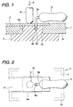
- Fig. 1 is a vertically sectional side view showing a state on the way of manufacture of a first embodiment of the invention.
- Fig. 2 is a plan view of the state.
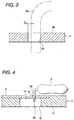
- Fig. 3 is an enlarged vertically sectional side view of a terminal.
- Fig. 4 is a vertically sectional side view showing the state after connection.
- Fig. 5 is a view corresponding to Fig. 1 showing a second embodiment of the invention.
- Fig. 6 is a view corresponding to Fig. 2 showing the second embodiment of the invention.
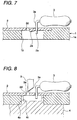
- Fig. 7 is a view corresponding to Fig. 4 showing a third embodiment of the invention.
- Fig. 8 is a view corresponding to Fig. 1 showing the third embodiment of the invention.
- Fig. 9 is a view correspond to Fig. 2 showing the third embodiment of the invention.
- Fig. 4 shows the state where a contact 3a of a resistor 3 as a circuit element is connected to a terminal 2 of a circuit board 1.
- the terminal 2 of a thin metallic plate e.g. a copper plate having a thickness of 0.64 mm
- the terminal 2 has a contact through-hole 2a.
- the board body 1 has a large hole area 1b for arranging a receiving part in an area corresponding to the terminal through-hole 2a.
- the terminal 2 is covered with an oxidation preventing (passivation) film 2b (e.g. tinning) as shown in Fig. 3.
- the oxidation preventing film 2b is formed after the contact through-hole 2a is formed. Therefore, the oxidation preventing film 2b is also formed on the inner surface of the contact through-hole 2a.
- a gap G between the inner surface of the contact through-hole 2a and the contact 3a (Fig. 3) is preferably 0.1 - 0.3 mm.
- the board 1 is arranged so that the hole area 1b is fit over the receiving portion 4a which is a convex portion of a receiving die 4.
- the upper surface of the receiving portion 4a is adapted to receive the lower surface of the edge of the contact through-hole 2a.
- the receiving portion 4a has a contact clearance concave portion 4b at the position corresponding to the contact through-hole 2a.
- the contact 3a of the resistor 3 is inserted into the contact through-hole 2a.
- the vicinity of the terminal through-hole 2a in the terminal 2 is crushed by a crushing punch 5 which is moved for pressing in a direction of arrow A, and plastically deformed as shown in Fig. 4, that is, a concave portion 11 is formed on the vicinity of the terminal through-hole 2a by a crushing punch 5.
- receiving portion 4a prevents the terminal 2 from projecting in the direction of the arrow A, the energy generated by the deforming process can not be consumed by forming a deformation in the direction of the arrow A. Therefore, the energy goes toward the terminal through-hole 2a and is consumed by forming a convex contact portion 10 projected from a part of the contact through-hole 2a. So that the terminal 2 is mechanically and electrically connected to the contact 3a. Thereafter, the receiving die 4 is taken off.
- the terminal 2 since the terminal 2 is plastically deformed so that it is connected to the contact 3a of the resistor 2, it does not take a long time for connection. In addition, a troublesome operation of setting/adjusting a current value and pressure is not required, and the connection can be made easily for a short time.
- the stroke of the crushing punch 5 has only to be controlled to make the plastic deformation which is appropriate for connection, thereby making sure connection in a simple step.
- Figs . 5 and 6 show the second embodiment of this invention. This embodiment is different from the first embodiment in the following point.
- plural (e.g. three) punches 6, 7 and 8 are provided for punching the vicinity (periphery) of the contact through-hole 2a in the terminal 2 at plural (e.g. three) points.
- slit-like deformation clearance holes 2c, 2c, 2c are previously formed.
- the periphery of the contact through-hole 2a in the terminal 2 is crushed and deformed at three points by these punches 6, 7 and 8 so that the edge of the. contact through-hole 2a is mechanically and electrically connected to the contact 3a.
- the terminal 2 since the terminal 2 has deformation clearance slits 2c, 2c and 2c,. the plastic deformation will not be extended to the outside of each slit.
- the deformation clearance slits 2c can be omitted.
- a single punch may be provide to press/crush the terminal at the plural points. The number of crushing points is not limited.
- Figs. 7 to 9 show the third embodiment of this embodiment. This embodiment is different from the first embodiment in the following point.
- Fig. 7 shows the state where connection has been completed.
- Figs. 8 and 9 show the state before connection.
- the terminal 2 has a punch contacting slit 2d having e.g. a square shape for facilitating the plastic deformation which is formed to align with the contact through-hole 2a.
- the punch 9 has a slanted tip, and the longitudinal width Wa of the punch contacting slit 2d is set to be slightly larger than that of the punch 9 (Fig. 9).
- the receiving portion 4a of the receiving die 4 has a concave portion 4c for clearance of the punch and contact.
- the punch 9 is caused to descend so that its slope 9a is brought into contact with the right edge of the punch contacting slit 2d (in the vicinity of the contact through-hole 2a). Then, this right edge is pressed down while it is compressed toward the contact so that it is plastically deformed.
- the terminal 2 is mechanically and electrically connected to the contact 3a.
- the plastically deformed portion is denoted by reference symbol 2e.
- the plastic deformation can be made comparatively easily.
- the contact 3a is brought into contact with this portion, thereby assuring the electric connection therebetween.
- the circuit element is a resistor as an example, but it may be a capacitor or any other discrete component.
Landscapes
- Engineering & Computer Science (AREA)
- Manufacturing & Machinery (AREA)
- Microelectronics & Electronic Packaging (AREA)
- Metallurgy (AREA)
- Apparatuses And Processes For Manufacturing Resistors (AREA)
- Manufacturing Of Electrical Connectors (AREA)
- Details Of Resistors (AREA)
- Coupling Device And Connection With Printed Circuit (AREA)
Abstract
Description
Claims (8)
- A method of connecting a contact of a circuit element to a terminal of a metallic plate, said method comprising the steps of:forming a contact through-hole in the terminal;inserting the contact into the contact through-hole; andplastically deforming a vicinity of the contact through-hole so that the terminal is connected to the contact.
- The method of connecting the contact to the terminal according to claim 1, wherein the vicinity of the contact through-hole is plastically deformed by a crushing punch.
- The method of connecting the contact to the terminal according to claim 2, wherein the crushing punch has a slanted tip surface.
- The method of connecting the contact to the terminal according to claim 1 further comprising the step of:
forming a deformation clearance hole opposite to the contact through-hole with respect to the vicinity of the contact through-hole prior to said plastically deforming step. - The method of connecting the contact to the terminal according to claim 1 further comprising the step of:
forming an oxidation preventing film on the terminal after said contact through-hole forming step. - A method of connecting a contact of a circuit element to a terminal of a metallic plate, said method comprising the steps of:forming a contact through-hole in the terminal;arranging the terminal on a receiving portion so that a vicinity of the contact through-hole is supported by the receiving portion;inserting the contact into the contact through-hole; andcrashing the vicinity of the contact through-hole by a crushing punch so that the terminal is connected to the contact.
- The method of connecting the contact to the terminal according to claim 6, wherein the crushing punch crashes the vicinity of the contact through-hole in a direction in which the receiving portion supports the terminal.
- The method of connecting the contact to the terminal according to claim 6, wherein said receiving portion has a contact clearance concave portion at a position corresponding to the contact through-hole.
Applications Claiming Priority (2)
| Application Number | Priority Date | Filing Date | Title |
|---|---|---|---|
| JP2000023962 | 2000-02-01 | ||
| JP2000023962A JP2001212631A (en) | 2000-02-01 | 2000-02-01 | Connecting method for circuit element |
Publications (2)
| Publication Number | Publication Date |
|---|---|
| EP1133011A2 true EP1133011A2 (en) | 2001-09-12 |
| EP1133011A3 EP1133011A3 (en) | 2004-11-10 |
Family
ID=18550038
Family Applications (1)
| Application Number | Title | Priority Date | Filing Date |
|---|---|---|---|
| EP01101740A Withdrawn EP1133011A3 (en) | 2000-02-01 | 2001-01-25 | Method of connecting circuit element |
Country Status (3)
| Country | Link |
|---|---|
| US (1) | US6725537B2 (en) |
| EP (1) | EP1133011A3 (en) |
| JP (1) | JP2001212631A (en) |
Families Citing this family (5)
| Publication number | Priority date | Publication date | Assignee | Title |
|---|---|---|---|---|
| JP2001212631A (en) * | 2000-02-01 | 2001-08-07 | Tokai Rika Co Ltd | Connecting method for circuit element |
| FR2848731B1 (en) * | 2002-12-16 | 2007-05-25 | Mecelec Ind | ELECTRICAL CONNECTOR AND METHOD FOR MANUFACTURING THE SAME |
| US6913454B2 (en) * | 2003-07-08 | 2005-07-05 | Skh Technologies Llc | Apparatus and method for attaching filamentary members to a substrate |
| DE10344261A1 (en) * | 2003-09-23 | 2005-05-04 | Endress & Hauser Gmbh & Co Kg | Printed circuit board with a holding device for holding wired electronic components, method for producing such a printed circuit board and its use in a soldering oven |
| CN111760983B (en) * | 2020-06-18 | 2022-08-19 | 浙江路源科技有限公司 | Printed board terminal riveting tool |
Family Cites Families (24)
| Publication number | Priority date | Publication date | Assignee | Title |
|---|---|---|---|---|
| US3605244A (en) * | 1966-04-20 | 1971-09-20 | Electrovert Mfg Co Ltd | Soldering methods and apparatus |
| US3750278A (en) * | 1970-07-17 | 1973-08-07 | Sylvania Electric Prod | Printed circuit board with through connection and method and machine for making the through connection |
| US3934327A (en) * | 1974-08-16 | 1976-01-27 | Hafner Otto P | Method of interlocking overlapping sheet material |
| US3977074A (en) * | 1975-02-06 | 1976-08-31 | General Motors Corporation | Double sided printed circuit board and method for making same |
| US4059897A (en) * | 1975-09-15 | 1977-11-29 | Robertshaw Controls Company | Method of joining thin and thick switch members |
| FR2337600A1 (en) * | 1976-01-09 | 1977-08-05 | Creusot Loire | PROCEDURE AND INSTALLATION FOR MANUFACTURING A WAITING TUBING ON A VERY VERY THICKNESS WALL |
| US4073561A (en) * | 1976-11-18 | 1978-02-14 | Baranowski Conrad J | Method for forming a heat sink and connector device and the product thereof |
| US4458414A (en) * | 1981-12-24 | 1984-07-10 | Sangamo Weston, Inc. | Method of manufacturing a low leakage capacitor header |
| JPS63211692A (en) * | 1987-02-27 | 1988-09-02 | 株式会社日立製作所 | Double-sided interconnection board |
| US5192995A (en) * | 1988-08-26 | 1993-03-09 | Semiconductor Energy Laboratory Co., Ltd. | Electric device utilizing antioxidation film between base pad for semiconductor chip and organic encapsulating material |
| US5082460A (en) * | 1989-10-02 | 1992-01-21 | Zierick Manufacturing Corporation | Electrical terminal with frangible mounting leg and method of forming the same |
| US5083362A (en) * | 1990-12-13 | 1992-01-28 | Briggs & Stratton Corp. | Method for making a vehicle anti-theft key with resistor |
| JPH0563357A (en) * | 1991-09-05 | 1993-03-12 | Toshiba Corp | Manufacturing method of metal core printed wiring board |
| JPH05290666A (en) * | 1992-04-10 | 1993-11-05 | Tanaka Kikinzoku Kogyo Kk | Method of manufacturing electric contact |
| US5861577A (en) * | 1992-06-05 | 1999-01-19 | Hitachi Construction Machinery Co., Ltd. | Seal structure for member-passing-through hole bored in metal partition member |
| US5497546A (en) * | 1992-09-21 | 1996-03-12 | Matsushita Electric Works, Ltd. | Method for mounting lead terminals to circuit board |
| EP0716563A3 (en) * | 1994-12-05 | 1997-12-10 | Siemens Aktiengesellschaft | Process for connecting the lead of an electric component and device manufactured by this process |
| US5579568A (en) * | 1995-02-08 | 1996-12-03 | Johnson Service Company | Method for mounting mechanical elements to a plate |
| US5692294A (en) * | 1995-06-09 | 1997-12-02 | The Whitaker Corporation | Tools for crimping an electrical contact onto a conductor |
| US5882159A (en) * | 1996-08-16 | 1999-03-16 | Profil Verbindungstechnik, Gmbh & Co. | Element, method of attaching the element to a plate-like component, component assembly and die button |
| EP0813268A1 (en) * | 1996-06-10 | 1997-12-17 | UNITED TECHNOLOGIES AUTOMOTIVE, Inc. | Interlocking terminal connection |
| US5899757A (en) * | 1997-11-03 | 1999-05-04 | Intercon Systems, Inc. | Compression connector |
| JP2000251979A (en) * | 1999-02-26 | 2000-09-14 | Shizuki Electric Co Inc | Pin-shaped terminal connection structure and terminal plate |
| JP2001212631A (en) * | 2000-02-01 | 2001-08-07 | Tokai Rika Co Ltd | Connecting method for circuit element |
-
2000
- 2000-02-01 JP JP2000023962A patent/JP2001212631A/en not_active Withdrawn
-
2001
- 2001-01-25 EP EP01101740A patent/EP1133011A3/en not_active Withdrawn
- 2001-01-25 US US09/768,553 patent/US6725537B2/en not_active Expired - Fee Related
Also Published As
| Publication number | Publication date |
|---|---|
| JP2001212631A (en) | 2001-08-07 |
| US20010012800A1 (en) | 2001-08-09 |
| US6725537B2 (en) | 2004-04-27 |
| EP1133011A3 (en) | 2004-11-10 |
Similar Documents
| Publication | Publication Date | Title |
|---|---|---|
| US5184767A (en) | Non-wicking solder preform | |
| US20030013330A1 (en) | Connector and method for manufacturing same | |
| US4497105A (en) | Method of manufacturing solid electrolyte chip capacitors | |
| WO2005096683A1 (en) | Circuit board, its manufacturing method, and joint box using circuit board | |
| GB1588659A (en) | Attachment of terminal members in substrates bearing electrical circuits | |
| US6406338B1 (en) | Board terminal and method of producing same | |
| US6725537B2 (en) | Method of connecting circuit element | |
| US20020002007A1 (en) | Board terminal and method of producing same | |
| JP2002093489A (en) | Conduction method of ultra-thin laminate and sheet electrode | |
| US7439625B2 (en) | Circuit board | |
| JP3846987B2 (en) | Manufacturing method of chip resistor | |
| JPH06163300A (en) | Terminal connection structure for electrical parts | |
| US5933946A (en) | Process for providing an electronic module with a cover and terminal pins | |
| CN111869334B (en) | Method for manufacturing printed circuit board using conductor component mold | |
| EP0259925A1 (en) | A method of interconnecting metal strips for use in electrical components, and electrical component comprising strips thus interconnected | |
| US6751860B2 (en) | Method of making of electronic parts mounting board | |
| JP3355470B2 (en) | Structure and method for fixing metal terminal to another member | |
| JP2003009335A (en) | Connection structure of flat wire, and end treatment method of the flat wire | |
| JPH0420785B2 (en) | ||
| JP2736589B2 (en) | Contact and manufacturing method thereof | |
| JP3234727B2 (en) | Circuit board manufacturing method | |
| US5189275A (en) | Printed circuit assembly with contact dot | |
| JPH02285602A (en) | Electronic part | |
| JPH0963388A (en) | Terminal for electronic part and its manufacture | |
| JPH0521097A (en) | Printed circuit board terminal structure |
Legal Events
| Date | Code | Title | Description |
|---|---|---|---|
| PUAI | Public reference made under article 153(3) epc to a published international application that has entered the european phase |
Free format text: ORIGINAL CODE: 0009012 |
|
| AK | Designated contracting states |
Kind code of ref document: A2 Designated state(s): AT BE CH CY DE DK ES FI FR GB GR IE IT LI LU MC NL PT SE TR |
|
| AX | Request for extension of the european patent |
Free format text: AL;LT;LV;MK;RO;SI |
|
| PUAL | Search report despatched |
Free format text: ORIGINAL CODE: 0009013 |
|
| AK | Designated contracting states |
Kind code of ref document: A3 Designated state(s): AT BE CH CY DE DK ES FI FR GB GR IE IT LI LU MC NL PT SE TR |
|
| AX | Request for extension of the european patent |
Extension state: AL LT LV MK RO SI |
|
| RIC1 | Information provided on ipc code assigned before grant |
Ipc: 7H 05K 3/32 B Ipc: 7H 01R 4/10 B Ipc: 7H 01R 12/34 A |
|
| AKX | Designation fees paid | ||
| REG | Reference to a national code |
Ref country code: DE Ref legal event code: 8566 |
|
| STAA | Information on the status of an ep patent application or granted ep patent |
Free format text: STATUS: THE APPLICATION IS DEEMED TO BE WITHDRAWN |
|
| 18D | Application deemed to be withdrawn |
Effective date: 20050511 |