EP1132970A2 - Power semiconductor element capable of improving short circuit withstand capability while maintaining low on-voltage and method of fabricating the same - Google Patents
Power semiconductor element capable of improving short circuit withstand capability while maintaining low on-voltage and method of fabricating the same Download PDFInfo
- Publication number
- EP1132970A2 EP1132970A2 EP01104596A EP01104596A EP1132970A2 EP 1132970 A2 EP1132970 A2 EP 1132970A2 EP 01104596 A EP01104596 A EP 01104596A EP 01104596 A EP01104596 A EP 01104596A EP 1132970 A2 EP1132970 A2 EP 1132970A2
- Authority
- EP
- European Patent Office
- Prior art keywords
- base layer
- layer
- forming
- impurity concentration
- emitter
- Prior art date
- Legal status (The legal status is an assumption and is not a legal conclusion. Google has not performed a legal analysis and makes no representation as to the accuracy of the status listed.)
- Withdrawn
Links
Images















Classifications
-
- H—ELECTRICITY
- H10—SEMICONDUCTOR DEVICES; ELECTRIC SOLID-STATE DEVICES NOT OTHERWISE PROVIDED FOR
- H10D—INORGANIC ELECTRIC SEMICONDUCTOR DEVICES
- H10D30/00—Field-effect transistors [FET]
- H10D30/60—Insulated-gate field-effect transistors [IGFET]
- H10D30/64—Double-diffused metal-oxide semiconductor [DMOS] FETs
- H10D30/66—Vertical DMOS [VDMOS] FETs
- H10D30/668—Vertical DMOS [VDMOS] FETs having trench gate electrodes, e.g. UMOS transistors
-
- H—ELECTRICITY
- H10—SEMICONDUCTOR DEVICES; ELECTRIC SOLID-STATE DEVICES NOT OTHERWISE PROVIDED FOR
- H10D—INORGANIC ELECTRIC SEMICONDUCTOR DEVICES
- H10D12/00—Bipolar devices controlled by the field effect, e.g. insulated-gate bipolar transistors [IGBT]
- H10D12/01—Manufacture or treatment
- H10D12/031—Manufacture or treatment of IGBTs
- H10D12/032—Manufacture or treatment of IGBTs of vertical IGBTs
- H10D12/038—Manufacture or treatment of IGBTs of vertical IGBTs having a recessed gate, e.g. trench-gate IGBTs
-
- H—ELECTRICITY
- H10—SEMICONDUCTOR DEVICES; ELECTRIC SOLID-STATE DEVICES NOT OTHERWISE PROVIDED FOR
- H10D—INORGANIC ELECTRIC SEMICONDUCTOR DEVICES
- H10D12/00—Bipolar devices controlled by the field effect, e.g. insulated-gate bipolar transistors [IGBT]
- H10D12/411—Insulated-gate bipolar transistors [IGBT]
-
- H—ELECTRICITY
- H10—SEMICONDUCTOR DEVICES; ELECTRIC SOLID-STATE DEVICES NOT OTHERWISE PROVIDED FOR
- H10D—INORGANIC ELECTRIC SEMICONDUCTOR DEVICES
- H10D12/00—Bipolar devices controlled by the field effect, e.g. insulated-gate bipolar transistors [IGBT]
- H10D12/411—Insulated-gate bipolar transistors [IGBT]
- H10D12/441—Vertical IGBTs
-
- H—ELECTRICITY
- H10—SEMICONDUCTOR DEVICES; ELECTRIC SOLID-STATE DEVICES NOT OTHERWISE PROVIDED FOR
- H10D—INORGANIC ELECTRIC SEMICONDUCTOR DEVICES
- H10D12/00—Bipolar devices controlled by the field effect, e.g. insulated-gate bipolar transistors [IGBT]
- H10D12/411—Insulated-gate bipolar transistors [IGBT]
- H10D12/441—Vertical IGBTs
- H10D12/461—Vertical IGBTs having non-planar surfaces, e.g. having trenches, recesses or pillars in the surfaces of the emitter, base or collector regions
- H10D12/481—Vertical IGBTs having non-planar surfaces, e.g. having trenches, recesses or pillars in the surfaces of the emitter, base or collector regions having gate structures on slanted surfaces, on vertical surfaces, or in grooves, e.g. trench gate IGBTs
-
- H—ELECTRICITY
- H10—SEMICONDUCTOR DEVICES; ELECTRIC SOLID-STATE DEVICES NOT OTHERWISE PROVIDED FOR
- H10D—INORGANIC ELECTRIC SEMICONDUCTOR DEVICES
- H10D62/00—Semiconductor bodies, or regions thereof, of devices having potential barriers
- H10D62/10—Shapes, relative sizes or dispositions of the regions of the semiconductor bodies; Shapes of the semiconductor bodies
- H10D62/17—Semiconductor regions connected to electrodes not carrying current to be rectified, amplified or switched, e.g. channel regions
- H10D62/393—Body regions of DMOS transistors or IGBTs
-
- H—ELECTRICITY
- H10—SEMICONDUCTOR DEVICES; ELECTRIC SOLID-STATE DEVICES NOT OTHERWISE PROVIDED FOR
- H10D—INORGANIC ELECTRIC SEMICONDUCTOR DEVICES
- H10D12/00—Bipolar devices controlled by the field effect, e.g. insulated-gate bipolar transistors [IGBT]
- H10D12/01—Manufacture or treatment
- H10D12/031—Manufacture or treatment of IGBTs
- H10D12/032—Manufacture or treatment of IGBTs of vertical IGBTs
- H10D12/035—Etching a recess in the emitter region
-
- H—ELECTRICITY
- H10—SEMICONDUCTOR DEVICES; ELECTRIC SOLID-STATE DEVICES NOT OTHERWISE PROVIDED FOR
- H10D—INORGANIC ELECTRIC SEMICONDUCTOR DEVICES
- H10D12/00—Bipolar devices controlled by the field effect, e.g. insulated-gate bipolar transistors [IGBT]
- H10D12/411—Insulated-gate bipolar transistors [IGBT]
- H10D12/441—Vertical IGBTs
- H10D12/461—Vertical IGBTs having non-planar surfaces, e.g. having trenches, recesses or pillars in the surfaces of the emitter, base or collector regions
-
- H—ELECTRICITY
- H10—SEMICONDUCTOR DEVICES; ELECTRIC SOLID-STATE DEVICES NOT OTHERWISE PROVIDED FOR
- H10D—INORGANIC ELECTRIC SEMICONDUCTOR DEVICES
- H10D18/00—Thyristors
- H10D18/60—Gate-turn-off devices
- H10D18/65—Gate-turn-off devices with turn-off by field effect
- H10D18/655—Gate-turn-off devices with turn-off by field effect produced by insulated gate structures
-
- H—ELECTRICITY
- H10—SEMICONDUCTOR DEVICES; ELECTRIC SOLID-STATE DEVICES NOT OTHERWISE PROVIDED FOR
- H10D—INORGANIC ELECTRIC SEMICONDUCTOR DEVICES
- H10D62/00—Semiconductor bodies, or regions thereof, of devices having potential barriers
- H10D62/10—Shapes, relative sizes or dispositions of the regions of the semiconductor bodies; Shapes of the semiconductor bodies
- H10D62/113—Isolations within a component, i.e. internal isolations
- H10D62/115—Dielectric isolations, e.g. air gaps
- H10D62/116—Dielectric isolations, e.g. air gaps adjoining the input or output regions of field-effect devices, e.g. adjoining source or drain regions
Definitions
- the present invention relates to a power semiconductor element including a MOSFET (Metal Oxide Semiconductor Field Effect Transistor) used in a power inverter and a method of fabricating the same, particularly, to an element structure capable of improving the short circuit withstand capability and a method of fabricating the same.
- MOSFET Metal Oxide Semiconductor Field Effect Transistor
- the present invention is applied to, for example, an IGBT (Insulated Gate Bipolar Transistor) a power MOSFET, a MCT (MOS Controlled Thyristor), and an IEGT (Injection Enhanced Gate Transistor).
- the power source apparatus used in the field of the power electronics is required to be miniaturized and to exhibit a high performance. Therefore, in the power semiconductor element (switching element), vigorous efforts are being made in an attempt to improve the performance of the power source apparatus in respect of the improvements in the breakdown voltage, in the adaptability for the large current, in the reduction of the loss, in the withstand capability to the breakdown, and in the operating speed.
- a power IBGT excellent in the breakdown voltage and in the adaptability for the large current and capable of obtaining an ON-voltage lower than that of the power MOSFET is widely used as a power semiconductor element having a breakdown voltage not lower than about 300 V.
- the power IGBT is an element that is driven by a MOS gate.
- Widely known to the art are two kinds of the power IGBT, i.e., a power IGBT of a planar structure, in which a MOS gate is formed in the shape of a flat plate, and a power IGBT of a trench structure, in which the MOS gate is buried inside a trench.
- the trench IGBT has a trench-gate structure in which a large number of trench IGBT cells each including a channel region formed of the trench side wall are arranged on a semiconductor substrate.
- the trench IGBT is said to be advantageous over the planar IGBT in that the trench IGBT permits easily improving the performance (or permits decreasing the loss) by the reduction of the channel resistance.
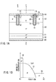
- FIG. 1A is a cross sectional view schematically showing the construction of a conventional trench IGBT.
- an n + -type buffer layer 11, an n - -type base layer 12, and a p-type base layer 13 are formed in the order mentioned on a p + -type collector layer 10.
- an n + -type emitter layer 14 is in a part of the surface region of the p-type base layer 13.
- a trench 15 extending downward from the surface of the emitter layer 14 to reach the n - -type base layer 12 through the emitter layer 14 and the p-type base layer 13.
- a gate electrode 17 (trench-gate electrode), which is covered with a gate insulating film 16, is buried in the trench 14. The trench-gate electrode 17 is withdrawn to reach, for example, a pad (not shown) for the gate electrode for contact with the outside.
- An emitter electrode 18 is formed to cover the emitter layer 14 and the p-type base layer 13.
- the emitter layer 14 and the p-type base layer 13 are electrically short-circuited by the emitter electrode 18.
- an insulating film 19 is formed on the trench-gate electrode 17.
- the trench-gate electrode 17 and the emitter electrode 14 are electrically isolated from each other by the insulating film 19.
- a collector electrode 20 is formed on the back surface of the collector region 10.
- a MOSFET is formed of the n - -type base layer 12, the p-type base layer 13, the emitter layer 14, the gate insulating film 16 and the trench-gate electrode 17. It should be noted that electrons are injected from the emitter layer 14 into the n - -type base layer 12 through a channel region CH formed in that region of the p-type base layer 13 which is in contact with the trench 15.
- FIG. 1B is a graph relating to an impurity concentration profile along the line X1-X2 shown in FIG. 1A and shows the impurity concentration distribution in the active area including the channel region CH.
- the profile includes the n-type impurity concentration distribution 30 in the emitter layer 14, the p-type impurity concentration distribution 31 in the p-type base layer 13, and the n-type impurity concentration distribution 32 in the n - -type base layer 12.
- the p-type impurity concentration in the p-type base layer 13 is increased to reach the highest concentration Cp0 in the position close to the junction between the emitter layer 14 and the p-type base layer 13, and the p-type impurity concentration is gradually lowered toward the n - -type base layer 12.
- the p-type base layer 13 is formed by diffusion in a surface region of the n - -type base layer 12 formed on the collector region 10 with an n-type buffer layer 11 formed therebetween. Then, a large number of n-type emitter layers 14 having a stripe pattern when viewed from above are formed in a surface region of the p-type base layer 13. As a result, the exposed portion of the p-type base layer 13 is allowed to have a large number of stripe pattern as viewed from above.
- the trench 15 having a stripe pattern as viewed from above are formed in each of the emitter layers 14 in a manner to extend to reach the n - type base layer 12.
- the trench 15 is formed to extend through the emitter layer 14 and the p-type base layer 13.
- the gate insulating film 16 such as a SiO 2 film is formed to cover the inner wall of the trench 15 and the upper surfaces of the emitter layer 14 and the p-type base layer 13.
- a polycrystalline silicon (polysilicon) film 17 containing P (phosphorus) is formed by a CVD (Chemical Vapor Deposition) method within the trench 15 and on the surfaces of the emitter layer 14 and the p-type base layer 13.
- the polysilicon film 17 is for formation of the trench-gate electrode.
- the polysilicon film 17 is patterned on the basis of the trench gate lead pattern so as to form a pad (not shown) for contact of the gate electrode. Also, the upper surface of the polysilicon film 17 within the trench 15 is etched back so as to permit the upper surface of the gate electrode 17 to be flush with the upper surfaces of the emitter layer 14 and the p-type base layer 13.
- an insulating film 19 is deposited on the upper surfaces of the trench 15, the emitter layer 14 and the p-type base layer 13, followed by forming a large contact hole for the lead of the gate electrode in the insulating film 19 formed on the pad for contact of the gate electrode. Also formed is a contact hole for the lead of the emitter-base in a manner to extend through the insulating film 19 around the opening of the trench 15 and through the gate insulating film 16 positioned below the insulating film 19.
- a metal wiring layer such as an aluminum wiring layer is formed by a sputtering method within the contact holes and on the insulating film 19 for the lead of the gate electrode and for the lead of the emitter-base, followed by patterning the metal wiring layer as desired so as to form an emitter electrode 18 and a gate electrode wiring (not shown).
- a collector electrode 20 is formed on the back surface of the collector layer 10, thereby forming the trench IGBT.
- a collector voltage VCE is applied between the collector electrode 20 and the emitter electrode 18.
- a positive gate voltage VGE is applied between the trench-gate electrode 17 and the emitter electrode 18.
- an inverted layer whose conductivity type is inverted from the p-type to the n-type is formed in the channel region CH of the p-type base layer 13. Electrons are injected from the emitter electrode 18 into the n - -type base layer 12 through the inverted layer, and the injected electrons are allowed to migrate through the n + -type buffer layer 11 to reach the p + -type collector layer 10.
- the power source voltage is applied to the collector electrode 20 when the IGBT is under the conductive state.
- a short circuit peak current I cp flows through the IGBT, with the result that the IGBT is broken down a certain time tsc later.
- the time between the short-circuiting of the load and the breakdown of the IGBT is called herein the short circuit withstand capability tsc. It has been confirmed that the short circuit withstand capability tsc is diminished with increase in the short circuit peak current I cp of the IGBT because of the thermal breakdown caused by the short circuit peak current.
- the conventional trench IGBT described above has the advantage that it is possible to increase the channel density so as to decrease the on-voltage. However, if the channel density is increased, the current flow is facilitated, with the result that the short circuit peak current I cp is increased and the short circuit withstand capability tsc is diminished. In other words, the on-voltage and the short circuit withstand capability have a trade-off relationship.
- the width of the contact opening is diminished, with the result that it is difficult to achieve the short circuit between the emitter layer 14 and the base layer 13 by the emitter electrode 18 in the entire surface in a direction parallel to the trench.
- the emitter layer 14 of the trench IGBT it is proposed to form the emitter layer 14 of the trench IGBT to have a ladder-like pattern as viewed from above. In other words, it is proposed to form the trench IGBT such that rectangular exposed portions of the base layer 13 are dotted.
- the trench IGBT such that the emitter layer 14 as a whole has a mesh-like (or a lattice-like) pattern or a mesh-like (or zigzag patterned lattice-like) pattern having an offset as viewed from above.
- a trench contact structure in which a trench for the emitter contact is formed in that portion of the base layer 13 which is positioned between the adjacent emitter layers 14, and the emitter electrode 18 is formed in contact with the side surface of the emitter layer 14 and with the base layer 13 within the trench.
- the on-voltage and the short circuit withstand capability have the trade-off relationship in the various trench IGBT's of the constructions described above, making it difficult to satisfy both the on-voltage and the short circuit withstand capability simultaneously.
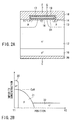
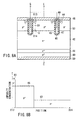
- FIG. 2A is a cross sectional view schematically showing the construction of the conventional IGBT of the planar gate type.
- an n - -type base layer 12 is formed on a p + -type collector layer 10, and a p-type base layer 13 is formed in a part of the surface region of the n - -type base layer 12.
- an n + -type emitter layer 14 is formed in a part of the surface region of the p-type base layer 13.
- a gate insulating film 16 is formed to cover the base layers 12, 13 positioned between the adjacent emitter layers 14, and a gate electrode 17 is formed on the gate insulating film 16.
- An emitter electrode 18 is formed on the other region. It should be noted that the emitter electrode 18 and the gate electrode 17 are electrically insulated from each other by the insulating film 19. Further, a collector electrode 20 is formed on the back surface of the collector region 10 so as to form an IGBT.
- FIG. 2B is a graph relating to an impurity concentration profile along the line Y1-Y2 shown in FIG. 2A and shows the impurity concentration distribution in the active area including the channel region CH.
- the profile includes the n-type impurity concentration distribution 30 in the emitter layer 14, the p-type impurity concentration distribution 31 in the p-type base layer 13, and the n-type impurity concentration distribution 32 in the n - -type base layer 12.
- the p-type impurity concentration in the p-type base layer 13 is increased to reach the highest concentration Cp0 in the position close to the junction between the emitter layer 14 and the p-type base layer 13, and the p-type impurity concentration is gradually lowered toward the n - -type base layer 12.
- planar IGBT differs from the trench IGBT in the gate construction. However, since the planar IGBT is equal to the trench IGBT in operation, the on-voltage and the short circuit withstand capability have the trade-off relationship in the planar IGBT, too, though the detailed description thereof is omitted.
- An object of the present invention is to provide a power semiconductor element capable of improving the short circuit withstand capability while maintaining a low on-voltage and a method of fabricating the particular power semiconductor element.
- a semiconductor element comprising:
- a semiconductor element comprising:
- a semiconductor element comprising:
- a method of fabricating a semiconductor element comprising the steps of:
- a method of fabricating a semiconductor element comprising the steps of:
- a method of fabricating a semiconductor element comprising the steps of:
- a method of fabricating a semiconductor element comprising the steps of:
- the second base layer positioned between the emitter layer and the first base layer and having a channel of a MOSFET formed therein has an impurity concentration profile such that the peak of the impurity concentration is positioned in the vicinity of the first base layer. Therefore, the pinch-off point of the channel region in the MOSFET is positioned closer to the first base layer than in the prior art. As a result, the voltage drop within the region between the pinch-off point and the channel edge is decreased in the voltage between the source region and drain region of the MOSFET or the voltage between the collector and the emitter of the IGBT.
- the voltage between the source region and drain region of the MOSFET or the voltage between the collector and the emitter of the IGBT is lowered, making it possible to lower the saturated current value of the drain current or the collector current in the event of the load short circuit. It follows that the present invention makes it possible to improve the short circuit withstand capability of the MOSFET or IGBT without affecting the on-voltage characteristics.
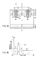
- an n + -type buffer layer 41, an n - -type base layer 42 having a high resistivity, a p + -type base layer 51 having a high impurity concentration, and a p-type base layer 43 having a low impurity concentration are formed in the order mentioned on one surface region of a p + -type collector layer 40.
- an n + -type emitter layer 44 is selectively formed in a part of the surface region of the p-type base layer 43.
- a trench 45 is formed to extend downward from the surface of the emitter layer 14 to reach the n - -type base layer 42 through the emitter layer 44, the p-type base layer 43 and the p + -type base layer 51.
- a gate electrode 47 (trench-gate electrode), which is covered with a gate insulating film 46, is buried in the trench 45.
- the emitter layer 44 is formed to have, for example, a striped pattern consisting of a plurality of columns as viewed from above, and the trench 45 is formed in a middle region of adjacent the emitter layers 14.
- each of the trench 45 and the trench-gate electrode 47 is also formed to have a striped pattern consisting of a plurality of columns as viewed from above.
- the p + -type collector layer 40 consists of a p + -type silicon substrate
- each of the n + -type buffer layer 41 and the n - -type base layer 42 consists of an epitaxially grown layer formed on the p + -type silicon substrate.
- an insulating film 49 is deposited on the p-type base layer 43 and the trench-gate electrode 47, and the emitter electrode 48 is formed to be in contact with a part of the emitter layer 44 and with a part of the p-type base layer 43 via a contact hole formed in the insulating film 49 for the lead of the emitter-base.
- each of the trench-gate electrode 47 is formed to extend to reach, for example, a gate contact pad (not shown), and a gate electrode wiring is formed in contact with the gate contact pad.
- a collector electrode 50 is formed on the back surface of the p + -type collector layer 40.
- the n + -type buffer layer 41 is intended to improve the breakdown voltage of the IGBT. Where the required breakdown voltage can be maintained by another method, it is possible to omit the n + -type buffer layer 41. This is also be case with the second embodiment, et seq. which are to be described herein later.
- a MOSFET is formed of the n - -type base layer 42, the p + -type base layer 51, the p-type base layer 43, the emitter layer 44, the gate insulating film 46 and the trench-gate electrode 47.
- electrons are injected from the emitter layer 44 into the n - -type base layer 42 through a channel region CH formed in those portions of the p + -type base layer 51 and the p-type base layer 43 which are in contact with the trench 45.
- FIG. 3B is a graph relating to the impurity concentration profile along the line X3-X4 shown in FIG. 3A and shows the impurity concentration distribution in the active region including the channel region CH.
- the impurity concentration profile includes the n-type impurity distribution 60 in the emitter layer 44, the p-type impurity concentration distribution 61 in the p-type base layer 43, the p-type impurity concentration distribution 62 in the p + -type base layer 51, and the n-type impurity concentration distribution 63 in the n - -type base layer 42.
- the highest concentration Cp1 of the p-type impurity in the p-type base region is formed in a position close to the junction between the p + -type base layer 43 and the n - -type base region 42, not in a position close to the junction between the emitter layer 44 and the p-type base layer 43.
- a collector voltage VCE is applied first between the collector electrode 50 and the emitter electrode 48.
- a predetermined positive gate voltage VGE is applied between the trench-gate electrode 47 and the emitter electrode 48.
- an inverted layer in which the conductivity is converted from the p-type to the n-type, is formed in the channel region CH of the p-type base layer 43 and the p + -type base layer 51.
- electrons are injected from the emitter electrode 48 into the n - -type base layer 42 through the inverted layer.
- the electrons thus injected are migrated through the n + -type buffer layer 41 to reach the p + -type collector layer 40. Since a forward bias is applied in this step between the p + -type collector layer 40 and the n - -type base layer 42, holes are injected from the p + -type collector layer 40 into the n - -type base layer 42. As a result of the injection of both electrons and holes into the n - -type base layer 42, modulation of the conductivity takes place within the n - -type base layer 42 so as to markedly lower the resistance of the n - -type base layer 42, thereby turning on the IGBT.
- the power source voltage is applied to the collector electrode 50 when the IGBT is under the conductive state.
- a short circuit peak current I cp flows through the IGBT, with the result that the IGBT is broken down a certain time tsc later.
- the time between the short-circuiting of the load and the breakdown of the IGBT is called herein the short circuit withstand capability tsc. It has been confirmed that the short circuit withstand capability tsc is diminished with increase in the short circuit peak current I cp of the IGBT because of the thermal breakdown caused by the short circuit peak current.
- the IGBT according to this embodiment permits diminishing the saturated current value while maintaining the static characteristics of the collector current of the conventional IGBT. As a result, it is possible to increase the short circuit withstand capability.
- the reason for the improvement of the short circuit withstand capability is as follows.
- the collector voltage VCE of the IGBT under the on-state is further increased, the potential of the channel region CH of the p-type base layer is also increased, with the result that the difference between the gate potential and the base potential is made smaller than the threshold voltage of the MOSFET.
- the threshold voltage is increased in the region near the emitter layer having a high impurity concentration, the phenomenon described above is rendered prominent, thereby making it impossible to maintain the inverted layer.
- the channel region is depleted (pinch-off) and the resistance of the channel region is rendered infinitely high so as to permit the current of the IGBT to be saturated.
- the pinch-off takes place in the region near the emitter layer where the p-type impurity has the highest concentration.
- the threshold voltage is determined by the p + -type base layer 51 having the impurity concentration higher than that of the p-type base layer 43 and, thus, the pinch-off phenomenon also takes place in the p + -type base layer 51 having a high impurity concentration.
- the p + -type base layer 51 is formed in a location deeper than the junction between the emitter layer 44 and the p-type base layer 43. In other words, the pinch-off point is located closer to the n-type base layer in the present invention than in the prior art.
- the pinch-off point is controlled by forming the p + -type base layer 43.
- the significance of the particular control will now be described in detail with reference to the graph of FIG. 3C.
- the position in the depth direction as measured from the boundary between the emitter electrode and the emitter layer, is plotted in the abscissa.
- the voltage as measured on the basis of the voltage at the boundary between the emitter electrode and the emitter layer, is plotted on the ordinate of the graph.
- the voltage distribution over the various regions is plotted in the graph of FIG. 3C in respect of the conventional IGBT and the IGBT according to this embodiment of the present invention.
- the point in the depth direction is plotted simply as a model on the abscissa of the graph.
- the emitter layer is actually formed very thin, compared with, for example, the p-type base layer.
- the pinch-off point is set in a p-type base layer having a high impurity concentration.
- the pinch-off point is set to reside in substantially the boundary between the p-type base layer and the n-type base layer.
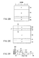
- FIG. 3D shows the result of simulation of the static characteristics in terms of the relationship between the collector voltage and the collector current in respect of the conventional IGBT and the IGBT according this embodiment of the present invention.
- the saturation current value of the IGBT according to this embodiment is lower than that of the conventional IGBT. It follows that it is possible in the present invention to suppress the amount of heat generated by the saturation current, making it possible to improve the short circuit withstand capability.
- the peak of the impurity concentration in the p-type base layer 13 resides in a point 0.5 ⁇ m deep from the boundary between the p-type base layer 13 and the emitter layer 14 in the conventional trench IGBT.
- the saturation value of the current of the IGBT in this case was 2300 A/cm 2 and the short circuit withstand capability was not higher than 1 ⁇ s.
- the trench IGBT according to this embodiment of the present invention makes it possible to improve the short circuit withstand capability without affecting the on-voltage characteristics.
- planar patterns of the emitter region and the exposed portion of the base region (contact region with the emitter electrode) of the trench IGBT are equal to the patterns of FIG. 1A described previously in conjunction with the prior art. However, it is possible to modify these planar patterns in various fashions.
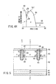
- FIG. 4A is a cross sectional view schematically showing a trench IGBT, which is directed to the construction of a power semiconductor element according to the second embodiment of the present invention.
- the p + -type base layer 51 in the first embodiment is arranged within the p-type base layer 43 in the depth direction.
- an n + -type buffer layer 41, an n - -type buffer layer 41 having a high resistivity, and a p-type base layer 43 having a low impurity concentration are formed in the order mentioned on one surface region of a p + -type collector layer 40.
- a p + -type base layer 51 is formed within the p-type base layer 43, and an n + -type emitter layer 44 is selectively formed in a part of the surface region of the p-type base layer 43.
- a trench 45 is formed to extend downward from the surface of the emitter layer 44 to reach the n - -type base layer 42 through the emitter layer 44, and the p-type and p + -type base layers 43, 51 and 43.
- a gate electrode 47 (trench-gate electrode), which is covered with a gate insulating film 46, is buried in the trench 45.
- the construction of the other portion is exactly equal to that described previously in conjunction with the first embodiment and, thus, the description thereof is omitted herein.
- FIG. 4B is a graph relating to the impurity concentration profile along the line X5-X6 shown in FIG. 4A and shows the impurity concentration distribution in the active region including the channel region CH.
- the impurity concentration profile shown in FIG. 4B includes the n-type impurity concentration distribution 60 in the emitter layer 44, the p-type impurity concentration distribution 61 in the p-type base layer 43, the p-type impurity concentration distribution 62 in the p + -type base layer 51, and the n-type impurity concentration distribution 63 in the n - -type base layer 42.
- the point of the highest concentration Cp1 of the p-type impurity concentration in the p-type base region resides in substantially the center in the depth direction of the p-type base layer 43.
- the operation of the IGBT in the second embodiment is substantially equal to that described previously in conjunction with the first embodiment.
- the threshold voltage is determined by the portion of the p + -type base layer 51 having a high impurity concentration, and the pinch-off phenomenon takes place within the p + -type base layer 51.
- FIG. 4C shows the voltage distribution over the various regions as in the first embodiment.
- V(pin-ch') is naturally smaller than the conventional V(pin-ch) and the relationship VCE(2) ⁇ VCE(3) ⁇ VCE(1) is established in terms of the relationship with the conventional construction and the construction described previously in conjunction with the first embodiment.
- the saturation current also has the relationship given above.
- the pinch-off point is set in substantially the center of the p-type base layer.
- the pinch-off point is not limited to the center of the p-type base layer.
- the requirements for the short circuit withstand capability differ in various fashions depending on the load element controlled by the IGBT. It is considered reasonable to state that it is most desirable in view of the process to obtain a desired short circuit withstand capability by controlling the position of the pinch-off point depending on the degree of the requirement as in the second embodiment.
- the second embodiment is featured in that the pinch-off phenomenon is generated in a deeper position than in the prior art, as in the first embodiment.
- the second embodiment is featured in that formed is the p + -type base layer 51 having an impurity concentration distribution having a maximum value Cp1 of the impurity concentration higher than a maximum value Cp2 of the impurity concentration within the p-type base layer 43 in a position deeper than the position of the maximum value Cp2.
- FIGS. 4D and 4E show the impurity concentration profiles in which the p-type base layer 43 and the p + -type base layer 51 are regarded as a single layer.
- FIG. 4D shows the impurity concentration profile having the highest impurity concentration Cp1 in substantially the center of the p-type base layer.
- FIG. 4E shows that the impurity concentration 64 within the p-type base layer is increased with increase in the depth so as to reach the maximum value Cp1 in the vicinity of the boundary with the n - -type base layer.
- the impurity concentration profile shown in each of FIGS. 4F and 4G consists of the overlapping of a profile in which the impurity concentration is diminished with increase in the depth of the p-type base layer 43 as in the conventional profile and a profile of the p + -type base layer 51 having the maximum value Cp1 larger than the maximum value Cp2 of the impurity concentration in the p-type base layer.
- the p-type base layer has two peaks Cp1 and Cp2 of the impurity concentration (Cp1 > Cp2). In this case, the effect of the second embodiment can be obtained by allowing the point of the maximum value Cp1 to be positioned deeper than the point of the maximum value Cp2.
- Table 1 shows the short circuit withstand capability, i.e., the time between the flow of the short circuit peak current Icp and the start up of the short circuit protection circuit of the element, covering the case where the p + -type base layer 51 or the position of the impurity concentration Cp1 is successively deepened by the distance of 0.5 ⁇ m. Specifically, it has been confirmed that it is possible to achieve 10 ⁇ s of the short circuit withstand capability, which is required in recent years, by setting the position of the p + -type base layer 51 or the position of the impurity concentration Cp1 at the position at least 1 ⁇ m deep from the surface of the p-type base layer 43.
- the ion implantation method and annealing which is widely used for forming an impurity diffusion layer, can also be used in the present invention for forming the p-type base layer. It is known to the art that, if the accelerating voltage of the impurity in the ion implantation step is increased, the concentration peak of the impurity is changed. Therefore, where the high concentration p + -type base 51 layer is formed by the ion implantation and annealing, it is necessary to set the accelerating voltage such that it is possible to obtain a desired short circuit withstand capability. Table 2 shows the result of simulation of the relationship between the accelerating voltage and the short circuit withstand capability. Accelerating voltage [keV] 60 100 300 500 600 Short circuit withstand capability [ ⁇ s] 0 6 11 14 15.5
- the highest concentration in the impurity concentration distribution in the channel region CH is formed in a position closer to the n - -type base layer 42 than the junction between the emitter layer 44 and the p-type base layer 43 in the second embodiment of the present invention.
- FIG. 4H shows the impurity concentration profile of the IGBT like FIGS. 4D to 4G.
- the impurity concentration distribution in the junction between the p-type base layer 43 and the emitter layer 44 is formed by the overlapping of the p-type impurity concentration distribution in the p-type base layers 43, 51 and the n-type impurity concentration distribution in the emitter layer 44. Therefore, the impurity concentration distribution in the junction noted above has a very sharp gradient ⁇ a.
- the p-type base layer has the highest concentration at the peak arrived at by the gradient ⁇ a.
- the highest concentration point of the p-type base layer is formed at a deeper position. As a result, a region having a moderate concentration gradient ⁇ b is included in the region between the region having the sharp gradient ⁇ a and the point of the highest concentration Cp1.
- the channel conductance between the pinch-off point Q having the highest impurity concentration of the p-type base layer 43 and the emitter layer 44 is defined as g1
- the channel conductance between the pinch-off point Q noted above and the n - -type base layer 42 is defined as g2.
- the voltage drop in the particular region is diminished, with the result that g2 is smaller than g1 (g2 ⁇ g1) in the IGBT of the conventional structure.
- the voltage V(pin-ch) owing to the resistance of the channel region between the pinch-off point Q and the n-type base layer 42 is removed by setting the pinch-off point Q within the high concentration p-type base layer 11. This is equal to the arrangement that g2 is set to be not smaller than g1 (g2 ⁇ g1).
- the channel conductance can be represented by the formula that the value obtained by integrating the carrier density induced within the channel with the length of the inverted layer is multiplied by W/L, where W represents the channel width and L denotes the channel length.
- W represents the channel width
- L denotes the channel length.
- the channel conductance is inversely proportional to the channel length. If the pinch-off point is moved toward the n - -type base layer 42 as in the second embodiment of the present invention, the channel length L in the channel conductance g2 is naturally diminished.
- g1 is diminished and g2 is enlarged if the pinch-off point is moved toward the n - -type base layer 42, with the result that the relationship between g2 and gl in the pinch-off point is reversed so as to satisfy the relationship of g2 ⁇ g1.
- the second embodiment of the present invention permits improving the short circuit withstand capability like the first embodiment described previously.
- FIG. 5 is a cross sectional view showing a trench IGBT according to the third embodiment of the present invention.
- a p + -type base layer 51 is formed in contact with an n - -type base layer 42 and with the trench 45 and only in the vicinity of the trench 45.
- the other construction is equal to that of each of the first and second embodiments described previously and, thus, the description thereof is omitted.
- the impurity concentration profile along the line X7-X8, i.e., along the n + -type emitter layer 44, the channel region CH, and the n - -type base layer 42, is equal to that shown in FIG. 3B, 4E or 4G.
- the operation of the IGBT shown in FIG. 5 is basically equal to that of the IGBT according to each of the first and second embodiments described previously.
- the threshold voltage of the MOSFET is determined by the p + -type base layer 51 having a high impurity concentration, the pinch-off phenomenon also takes place in the pinch-off point Q within the p + -type base layer 51.
- the channel conductance g1 between the emitter layer 44 and the pinch-off point Q is not larger than the channel conductance g2 between the pinch-off point Q and the n - -type base layer 42, i.e., g2 ⁇ g1.
- the third embodiment is featured in that the p + -type base layer 51 having an impurity concentration higher than that in the p + -type base layer 43 is formed within the p + -type base layer 43.
- the impurity concentration profile along the line X7-X8 is as shown in FIG. 4B, FIG. 4D or FIG. 4F.
- FIG. 6 is a cross sectional view showing a trench IGBT.
- the trench IGBT according to the fourth embodiment is substantially equal to that according to the first embodiment, except that the trench IGBT of the fourth embodiment is allowed to have a trench contact structure.
- a trench 52 extending through a p-type base layer 43 in a manner to have the bottom thereof positioned on the surface of or within a p + -type base layer 51 is formed between the adjacent trenches 45.
- an emitter electrode 48 is buried in the trench 52. It should be noted that the emitter electrode 48 is in contact with not only the p-type base layer 43 but also the p + -type base layer 51 (trench contact).
- the impurity concentration profile along the line X9-X10 i.e., along the n + -type emitter layer 44, the channel region CH and the n - -type base layer 42, is substantially equal to that shown in FIG. 3B, FIG. 4E or FIG. 4G.
- the IGBT of the fourth embodiment shown in FIG. 6 also permits making the collector voltage VCE, at which the pinch-off phenomenon is generated, smaller than that in the prior art as in any of the first to third embodiments described above so as to suppress the saturation current value. It follows that it is also possible to improve the short circuit withstand capability in the fourth embodiment.
- the emitter electrode 48 is buried to reach a region in contact with the p + -type base layer 51, it is possible to suppress the operation of a parasitic transistor performed by the carrier injected into the n - -type base layer 42.
- the impurity concentration profile along the line X9-X10 is substantially equal to that shown in FIG. 4B, FIG. 4D or FIG. 4F.
- FIG. 7 is a cross sectional view showing a trench IGBT according to the fifth embodiment of the present invention.
- the IGBT according to the fifth embodiment of the present invention is substantially equal to that according to the fourth embodiment, except that, in the fifth embodiment, an n + -type emitter layer 44 is formed on the entire surface of a p-type base layer 43.
- the impurity concentration profile along the line X11-X12, i.e., along the emitter layer 44, the channel region CH, and the n - -type base layer 42 is substantially equal to that shown in FIG. 3B, FIG. 4E or FIG. 4G.
- the IGBT of the fifth embodiment shown in FIG. 7 also permits making the collector voltage VCE, at which the pinch-off phenomenon is generated, smaller than that in the prior art as in any of the first to fourth embodiments described above so as to suppress the saturation current value. It follows that it is also possible to improve the short circuit withstand capability in the fifth embodiment.
- the withstand capability of the IGBT to the latch-up occurrence can be improved in the fifth embodiment by employing the trench contact structure as in the fourth embodiment.
- the emitter electrode 48 and the emitter layer 43 are in contact with the side surface of the trench 52, making it possible to increase the contact areas of the trench 52 with the emitter electrode 48 and the emitter layer 43.
- the trench distance can be diminished so as to diminish the cell pitch and, thus, to improve the area efficiency of the IGBT.
- the impurity concentration profile along the line X11-X12 is substantially equal to that shown in FIG. 4B, FIG. 4D or FIG. 4F.
- FIGS. 8A and 8B show the impurity concentration profile along the line X13-X14 shown in FIG. 8A.
- the p-type base layer of the trench IGBT of the sixth embodiment is formed of only a p + -type base layer 53. Also, the impurity concentration distribution 65 of the p + -type base layer 53 is substantially constant in the depth direction.
- the threshold voltage of the MOSFET is not dependent on the position of the channel region CH and is constant over the entire channel region CH. Also, since the highest voltage is applied to that portion of the channel region CH which is in contact with the n - -type base layer 42, the pinch-off phenomenon is generated in the particular position. In other words, since it is possible to obtain the function exactly equal to that obtained in the first embodiment, it is possible to improve the short circuit withstand capability in the sixth embodiment, too.
- FIG. 9A is a cross sectional view showing a planar IGBT according to the seventh embodiment of the present invention
- FIG. 9B shows the impurity concentration distribution along the line Y3-Y4 shown in FIG. 9A.
- an n - -type base layer 42 is formed on the p + -type collector region 40, and a p-type base layer 43 is formed in a part of the surface region of the n - -type base layer 42.
- an n + -type emitter layer 44 is formed in a part of the surface region of the p-type base layer 43.
- a p + -type base layer 51 is formed within the p-type base layer in a manner to contact the n - -type base layer 42.
- a gate insulating film 46 is formed on the base layers 42, 43, and 51 positioned between the adjacent emitter layers 44, and a gate electrode 47 is formed on the gate insulating layer 46.
- An emitter electrode 48 is formed on the other region.
- the emitter electrode 48 thus formed is electrically insulated from the gate electrode 47 by the insulating film 49.
- a collector electrode 50 is formed on the back surface of the p + -type collector layer 40 so as to form an IGBT.
- the p + -type base layer 51 it is not absolutely necessary for the p + -type base layer 51 to be in contact with the n - -type base layer 42. It suffices for the p + -type base layer 51 to be present in the vicinity of the n - -type base layer 42.
- a MOSFET is formed by the n - -type base layer 42, the p + -type base layer 51, the p-type base layer 43, the n + -type emitter layer 44, the gate insulating film 46 and the gate electrode 47.
- electrons are injected from the emitter layer 44 into the n - -type base layer 42 through the channel region formed in the p-type base layers 43 and 51.
- FIG. 9B is a graph relating to the impurity concentration profile along the line Y3-Y4 shown in FIG. 9A and shows the impurity concentration distribution in the active region including the channel region CH.
- the impurity concentration profile includes the n-type impurity concentration distribution 60 in the emitter layer 64, the p-type impurity concentration distribution 61 in the p-type base layer 43, the p-type impurity concentration distribution 62 in the p + -type base layer 51, and the n-type impurity concentration distribution 63 in the n + -type base layer 42.
- the position where the p-type impurity concentration in the p-type base layer 43 forms the maximum concentration Cp2 is close to the junction between the emitter layer 44 and the p-type base layer 43, and the p-type impurity concentration is gradually lowered toward the n - -type base layer 42.
- the collector voltage VCE is applied between the collector electrode 50 and the emitter electrode 48.
- a predetermined positive gate voltage VGE is applied between the gate electrode 47 and the emitter electrode 48.
- an inverted layer (n-type channel), in which the conductivity is inverted from the p-type to the n-type, is formed in the channel region CH of the p-type base layers 43 and 51. Electrons are injected from the emitter electrode 48 into the n - -type base layer 42 through the inverted layer. The electrons thus injected are migrated to reach the p + -type collector layer 40.
- the power source voltage is applied to the collector electrode 50 when the IGBT is under the conductive state.
- a short circuit peak current I cp flows through the IGBT, with the result that the IGBT is broken down a certain time tsc later.
- the time between the short-circuiting of the load and the breakdown of the IGBT is called herein the short circuit withstand capability tsc. It has been confirmed that the short circuit withstand capability tsc is diminished with increase in the short circuit peak current I cp of the IGBT because of the thermal breakdown caused by the short circuit peak current.
- planar IGBT according to the seventh embodiment of the present invention permits diminishing the saturation current value while maintaining the static characteristics of the collector current of the conventional IGBT. As a result, it is possible to increase the short circuit withstand capability.
- the reason for the improvement of the short circuit withstand capability is as follows.
- the collector voltage VCE of the IGBT under the on-state is further increased, the potential of the channel region CH of the p-type base layer is also increased, with the result that the difference between the gate potential and the base potential is made smaller than the threshold voltage of the MOSFET.
- the threshold voltage is increased in the region near the emitter layer having a high impurity concentration, the phenomenon described above is rendered prominent, thereby making it impossible to maintain the inverted layer.
- the channel region is depleted (pinch-off) and the resistance of the channel region is rendered infinitely high so as to permit the current of the IGBT to be saturated.
- the pinch-off takes place in the region near the emitter layer where the p-type impurity has the highest concentration.
- the threshold voltage is determined by the portion of the p + -type base layer 51 having an impurity concentration higher than that in the p-type base layer 43 and, thus, the pinch-off phenomenon takes place in the p + -type base layer 51 having a high impurity concentration.
- the p + -type base layer 51 is positioned deeper than the junction between the emitter layer 44 and the p-type base layer 43. As a result, the voltage distribution in the longitudinal direction of the channel region CH is rendered equal to that shown in FIG. 3C described previously in conjunction with the first embodiment.
- the voltage drop caused by the resistance of the channel region CH is removed by setting the pinch-off point Q within the p + -type base layer 51 having a high impurity concentration.
- the channel conductance g1 between the pinch-off point Q within the p + -type base layer 51 and the n + -type emitter layer 44 is made not larger than the channel conductance g2 between the pinch-off point Q and the n - -type base layer 42, i.e., the relationship g2 ⁇ g1 is established, in contrast to the relationship g2 ⁇ g1 in the conventional structure.
- FIG. 10A is a cross sectional view showing a planar IGBT according to the eighth embodiment of the present invention
- FIG. 9B is a graph showing the impurity concentration profile in the depth direction along the line X15-X16 shown in FIG. 10A
- FIG. 9C is a graph showing the impurity concentration profile in the longitudinal direction of the channel region along the line Y5-Y6 shown in FIG. 10A.
- the IGBT according to the eighth embodiment of the present invention is substantially equal to the IGBT according to the seventh embodiment, except that, in the eighth embodiment, a p + -type base layer 51 is formed on the entire surface of the p-type base layer 43 sandwiched between the n + -type emitter layer 44 and the n - -type base layer 42 and in contact with the gate insulating film 46.
- the impurity concentration profile in the depth direction of the region ranging between the p + -type base layer 51 and the n - -type base layer is as shown in FIG. 10. Also, the impurity concentration profile in the longitudinal direction of the channel region ranging between the n + -type emitter layer 44 and the n - -type base layer 42 is as shown in FIG. 10C.
- 10B and 10C include the n-type impurity concentration distribution 60 in the n + -type emitter layer 44, the p-type impurity concentration distribution 61 in the p-type base layer 43, the p-type impurity concentration distribution 62 in the p + -type base layer 51, and the n-type impurity concentration distribution 63 in the n - -type base layer 52.
- the maximum impurity concentration in the p + -type base layer 51 is denoted by Cp1
- the maximum impurity concentration in the p-type base layer 43 is denoted by Cp2.
- a channel region CH is formed in the p + -base layer 51.
- the p + -type base layer 51 in which the channel region is formed has an impurity concentration higher than that in the adjacent p-type base layer 43 and has a constant impurity distribution in the longitudinal direction of the channel region. As a result, the pinch-off phenomenon takes place in the junction portion between the p + -type base layer 51 and the n - -type base layer 42.
- the voltage distribution in the channel region CH in the longitudinal direction of the channel region CH is equal to the distribution shown in FIG. 3C described previously in conjunction with the first embodiment.
- the voltage drop V(pin-ch) caused by the resistance in the channel region CH is removed by setting the pinch-off point Q within the p + -type base layer 51 having a high impurity concentration.
- the channel conductance gl between the pinch-off point Q of the p + -type base layer 51 and the n + -type emitter layer 44 is not larger than the channel conductance between the pinch-off point Q and the n - -type base layer 42, i.e., the relationship of g2 ⁇ g1 is established in contrast to the relationship of g2 ⁇ g1 in the prior art.
- VCE collector voltage
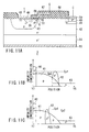
- FIG. 11A is a cross sectional view showing a lateral IGBT.
- an n - -type base layer 42 is formed on one surface of a p + -type semiconductor substrate layer 54.
- An n + -type buffer layer 41 and a p-type base layer 43 are selectively formed separately from each other in the surface of the n - -type base layer 42.
- a p + -type collector layer 40 is formed in the surface of the n + -type buffer layer 41, and an n + -type emitter layer 44 is formed in the surface of the p-type base layer 43.
- a p + -type base layer 51 having an impurity concentration higher than that in the p-type base layer 43 is formed in that region of the surface of the p-type base layer 43 which is in contact with the n - -type base layer 42.
- the p + -type base layer 51 it is not absolutely necessary for the p + -type base layer 51 to be in contact with the n - -type base layer 42 as far as the p + -type base layer 51 is positioned in the vicinity of the n - -type base layer 42.
- a gate insulating film 46 is formed on the surfaces of the p-type base layers 43, 51, the n - -type base layer 42 and the n + -type buffer layer 41, which are positioned between the p + -type collector region 40 and the n + -type emitter region 44.
- a gate electrode 47 is formed on the gate insulating film 46, and the gate electrode 47 is covered with an insulating film 49. Also formed is an emitter electrode 44 that is in contact with the n + -type emitter layer 44 and the p-type base layer 43 via a contact hole formed in the insulating film 49.
- a collector electrode 50 is formed on the p + -type collector layer 40, and an emitter electrode 55 is formed on the back surface of the p + -type substrate layer 54.
- the gate electrode 47 is electrically separated from the emitter electrode 48, the collector electrode 50, the n - -type base layer 42 and the p-type base layer 43 by the gate insulating film 46 and the insulating film 49.
- a MOSFET is formed of the n - -type base layer 42, the p + -type base layer 51, the p-type base layer 43, the emitter layer 44, the gate insulating film 46 and the gate electrode 47.
- electrons are injected from the emitter layer 44 into the n - -type base layer 42 through the channel region CH formed in the contact region of the p + -type and p-type base layers 51, 43 with the gate insulating film 46.
- FIG. 11B is a graph relating to the impurity concentration profile along the line Y7-Y8 shown in FIG. 11A and denotes the impurity concentration distribution in the active region including the channel region CH.
- the impurity concentration profile shown in FIG. 11A includes the n-type impurity concentration distribution 60 in the emitter layer 44, the p-type impurity concentration distribution 61 in the p-type base layer 43, the p-type impurity concentration distribution 62 in the p + -type base layer 51, and the n-type impurity concentration distribution 63 in the n - -type base layer 42.
- the maximum concentration Cp1 of the p-type impurity concentration within the p-type base layers (43, 51), which is positioned within the p + -type base layer 51, resides in the vicinity of the junction portion between the p + -type base layer 43 and the n - -type base layer, not in the vicinity of the junction portion between the emitter layer 44 and the p-type base layer 43.
- the operation of the lateral IGBT is basically equal to that of the trench IGBT described previously in conjunction with the first embodiment, except that, in the lateral IGBT, electrons and holes flow in the lateral direction into the p + -type collector layer 40 formed flush with the emitter layer 44, the p-type base layer 43 and the p + -type base layer 51, though electrons and holes flow in the vertical direction in the trench IGBT.
- a power source voltage is applied to the collector electrode 50 under the conductive state of the element, as described previously in conjunction with the first embodiment.
- a pinch-off phenomenon is generated, if the collector voltage VCE of the IGBT under the on-state is increased so as to exceed a certain threshold value.
- the pinch-off phenomenon takes place in the junction portion of the p-type base layer 43 with the emitter layer 44.
- the p + -type base layer 51 having a high impurity concentration is formed in the junction portion with the n - -type base layer 42.
- the threshold voltage of the MOSFET is determined by the p + -type base layer 51 rather than by the p-type base layer 43, with the result that the pinch-off phenomenon also takes place within the p + -type base layer 51.
- the voltage distribution within the channel region CH in the longitudinal direction of the channel region CH is as shown in FIG. 3C described previously in conjunction with the first embodiment.
- the voltage drop V(pin-ch) caused by the resistance of the channel region CH is removed by setting the pinch-off point Q within the p + -type base layer 51 having a high impurity concentration.
- the channel conductance between the pinch-off point Q within the p + -type base layer 51 and the emitter layer 44 is not higher than the channel conductance g2 between the pinch-off point Q and the n - -type base layer 42, i.e., the relationship of g2 ⁇ g1 is established in contrast to the relationship of g2 ⁇ g1 in the prior art.
- VCE collector voltage
- FIG. 11C is a graph relating to another example of the impurity concentration profile and shows the impurity concentration distribution in the case where the p + -type base layer 51 is formed not in contact with the n - -type base layer. Further, it is possible to form the gate portion on the side of the cathode by utilizing a trench, a gate insulating film and a gate electrode filling the trench, and an insulating film formed above the trench for insulating the gate electrode, as in the first embodiment.
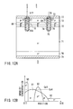
- FIG. 12A is a cross sectional view of a power MOSFET.
- the construction of the power MOSFET shown in FIG. 12A is substantially equal to that of the trench IGBT described previously in conjunction with the second embodiment of the present invention, except that the p + -type collector layer included in the second embodiment is not included in the embodiment shown in FIG. 12A, that the collector electrode in the second embodiment is converted into the drain electrode in the embodiment shown in FIG. 12, that the emitter layer included in the second embodiment is converted into the source layer in the embodiment shown in FIG. 12, and that the emitter electrode included in the second embodiment is converted into source electrode in the embodiment shown in FIG. 12.
- an n - -type base layer having a high resistivity and a p-type base layer 72 having a low impurity concentration are formed on one surface region of an n + -type drain layer 70.
- a p + -type base layer 80 having a high impurity concentration is formed within the p-type base layer 72, and an n + -type source layer 73 is selectively formed in a part of the surface region of the p-type base layer 72.
- a trench 74 extending from the surface of the source layer 73 to reach the n - -type base layer 71 through the source layer 73, the p-type and the p + -type base layers 72, 80 and 72.
- a gate electrode 76 (trench-gate electrode) covered with a gate insulating film 75 is buried in the trench 74.
- a source electrode 77 formed of, for example, an aluminum wiring.
- the source electrode 77 is electrically separated from the gate electrode 76 and serves to achieve short-circuiting between the n-type source layer 73 and the p-type base layer 72.
- an insulating film 78 is deposited on the p-type base layer 72 and the trench-gate electrode 76, and the source electrode 77 is formed so as to be in contact with both a part of the source layer 73 and a part of the base layer 72 via a contact hole formed in the insulating film 78 for the lead of the source ⁇ base layers.
- a drain electrode 79 is formed on the back surface of the n + -type drain layer 70, thereby forming a power MOSFET.
- electrons are injected from the source layer 73 into the n + -type drain layer 70 via the n - -type base layer 71. These electrons are allowed to migrate to reach the n + -type drain layer 70 through the channel region CH formed in those regions of the p + -type and p-type base layers 80, 72 which are in contact with the trench 74.
- FIG. 12B is a graph relating to the impurity concentration profile along the line X17-X18 shown in FIG. 12A, and shows the impurity concentration distribution in the active region including the channel region CH.
- the impurity concentration profile includes the n-type impurity concentration distribution 90 in the source layer 73, the p-type impurity concentration 91 in the p-type base layer 72, the p-type impurity concentration distribution 92 in the p + -type base layer 80, and the n-type impurity concentration distribution 93 in the n - -type base layer 71.
- the maximum concentration Cp3 of the p-type impurity concentration in the p-type base region is formed in a position deeper than the junction between the source layer 73 and the p-type base layer 72 (case 1).
- FIG. 12C exemplifies another impurity concentration profile.
- the maximum concentration Cp3 of the p-type impurity concentration within the p-type base region is positioned substantially in the vicinity of the boundary between the p-type base region and the n - -type base layer (case 2).
- a drain voltage VDS is applied between the drain electrode 79 and the source electrode 77.
- a predetermined positive gate voltage VGS is applied between the trench-gate electrode 76 and the source electrode 77.
- an inverted layer in which the conductivity is converted from the p-type to the n-type, is formed in the channel region CH of the p-type base layers 72 and 80.
- the electrons are migrated through the inverted layer such that the electrons flow from the source electrode 77 to reach the n + -type drain layer 70 through the n - -type base layer 71.
- a power source voltage is applied to the drain electrode 79 under the conductive state of the MOSFET. If the drain voltage VDS of the MOSFET under the on-state is increased, the voltage in the pinch-off point Q in the channel region of the p + -type base layer 80 is increased so as to make the potential difference between the gate potential and the base potential in the pinch-off point Q smaller than the threshold voltage. As a result, it is impossible to maintain the inverted layer so as to bring about the pinch-off phenomenon at the point Q. If the pinch-off phenomenon takes place in the prior art, it is impossible for the gate voltage to control the drain current. As a result, an excessively large drain current flows so as to breakdown the MOSFET. However, the short circuit withstand capability was not sufficient in the prior art.
- the threshold voltage of the MOSFET according to this embodiment of the present invention is determined by the p + -type base layer 80 having an impurity concentration higher than that in the p-type base layer 72, the pinch-off phenomenon takes place in the p + -type base layer 80. It should be noted that the p + -type base layer 80 is positioned deeper than the junction between the source layer 73 and the p-type base layer 72.
- the position where the pinch-off phenomenon is generated is controlled by the arrangement of the p + -type base layer 80.
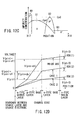
- the significance of the particular control will now be described with reference to the graph shown in FIG. 12D.
- the position in the depth direction on the basis of the boundary between the source electrode and the source layer is plotted on the abscissa.
- the voltage based on the reference voltage (ground point) at the boundary between the source electrode and the source layer is plotted on the ordinate.
- the voltage distribution over various regions are plotted in the graph of FIG. 12D in respect of the conventional power MOSFET and the power MOSFET according to this embodiment of the present invention (CASE1, CASE2).
- the abscissa is plotted simply as a model. In general, the source layer is actually formed very much thinner than the p-type base layer, etc.
- the p-type base layer is arranged so as to permit the pinch-off point Q to be positioned closer to the n-type base layer than in the prior art. Also, the voltage drop of V(pin) is generated between the boundary between the source electrode and the source layer and the pinch-off point Q. Also, the voltage drop V(pin-ch') is generated between the pinch-off point Q and the edge of the channel.
- VDS(2) V(pin) + V(pin-ch') + V(ch-D). It should be noted that, since the pinch-off point Q is positioned closer to the n - -type base layer than in the prior art, the value of V(pin-ch') is naturally smaller than the value of V(pin-ch) for the prior art. In other words, the relationship of VDS(2) ⁇ VDS(1) is established.
- the p + -base layer having a high impurity concentration is formed in contact with the n-type base layer. Therefore, the pinch-off point Q is positioned in substantially the boundary with the n-type base layer, with the result that it is possible to remove the voltage V(pin-ch) caused by the resistance of the channel region CH between the pinch-off point and the n-type base layer.
- VDS(3) ⁇ VDS(2) ⁇ VDS(1) is established in terms of the drain voltages of the conventional power MOSFET and the MOSFETs (cases 1 and 2) according this embodiment of the present invention.
- drain voltage VDS can be diminished by setting the pinch-off point in a deep position within the p-type base layer, it is possible to diminish the saturation value of the drain current because the saturation value of the collector current of MOSFET is basically changed in proportion to the drain voltage VDS.
- the channel conductance g3 between the pinch-off point Q of the p + -type base layer 80 and the n + -type source layer 73 is not larger than the channel conductance g4 between the pinch-off point Q and the n - -type base layer 71.
- the relationship of g4 ⁇ g3 is established in the power MOSFET of the present invention in contrast to the relationship of g4 ⁇ g3 for the prior art.
- VDS Drain voltage
- the technical idea of the present invention can also be applied to the case where the n-type drain layer 70 and the drain electrode 79 are formed flush with the n-type source layer 73 and the source electrode 77. Further, it is possible to apply the trench contact structure described previously in conjunction with the examples of IGBT to the MOSFET according to this embodiment of the present invention.
- the present invention makes it possible to improve the short circuit withstand capability of the power semiconductor elements such as IGBT and the power MOSFET without inviting deterioration of the on-voltage characteristics.
- the MOSFET has a threshold voltage that is lower at a position near the n-type base layer than at the junction between the emitter layer and p-type base layer. (hereinafter, this junction will be referred to as "point J1", shown in FIG. 3A and FIG. 3B.)
- the pinch-off voltage V(pin) is Vg + Vth(1), where Vg is the gate voltage and Vth(1) is the threshold voltage. If so, the potential Vth(a) at a position (hereinafter referred to as "point J2", shown in FIG. 3A and FIG. 3B), which is closer to the n-type base layer than the point J1, is V(pin) + V(ch), where V(ch) is the voltage drop that occurs in the p-type base layer.
- Vth(1) Vth(a) + V(ch).
- Vth(a) Vth(a) + V(ch).
- the threshold voltage is proportional to the impurity concentration.
- the impurity concentration at point J2 can be lower than the impurity concentration at point J1, by a value that corresponds to the voltage drop V(ch). Even if the impurity concentration at point J2 is lower than that at point J1, the pinch-off occurs at point J2, not point J1, so long as the difference in impurity concentration is less than the value corresponding to the voltage drop V(ch).
- the impurity concentration at point J2 is Cp1, while the impurity concentration at point J1 is Cp2.
- Cp1 the impurity concentration at point J2
- Cp2 the impurity concentration at point J1
- pinch-off can be caused in the region located near the n-type base layer and having the impurity concentration Cp1, not in the region having the impurity concentration Cp2, so long as the difference between Cp1 and Cp2 is less than the value that corresponds to the voltage drop that occurs in the channel region.
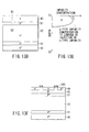
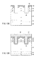
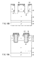
- FIGS. 13A, 13B, 13D and 13F to 13L are cross sectional views collectively showing the manufacturing process of the trench IGBT.
- FIGS. 13C and 13E show the impurity concentration profiles in the depth direction along the lines S1-S2 shown in FIGS. 13B and 13D, respectively.
- an n + -type buffer layer 41 and an n - -type base layer 42 are formed by the epitaxial growth on the surface of a p + -type silicon substrate (collector layer) 40, as shown in FIG. 13A.
- ions of a p-type impurities such as boron ions are implanted into a surface region of the n - -type base layer 42, followed by thermally diffusing the implanted boron ions, thereby forming a p-type base layer 103, as shown in FIG. 13B.
- FIG. 13C shows the impurity concentration profile in the p-type base layer 103 thus formed.
- FIG. 13E shows the impurity concentration profile in the p-type base layers 43 and 51.
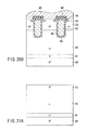
- a resist layer is laminated on the surface of the p-type base layer 43, followed by forming a resist pattern 100 consisting of a plurality of band-like openings arranged in parallel by the photolithography, as shown in FIG. 13F.
- n + -type emitter layers 44 are formed by implanting an n-type impurity into the surface region of the p-type base layer 43, with the resist pattern 100 used as a mask, followed by thermally diffusing the implanted n-type impurity.
- the resist pattern 100 is removed, followed by forming, for example, an oxide film 101 as a shielding film on the surfaces of the p-type base layer 43 and the emitter layers 44, as shown in FIG. 13G.
- a mask for the silicon etching having band-like openings narrower than the emitter regions 44 are formed on the surfaces of the n + -type emitter layers 44 by using the oxide film 101 thus formed, followed by applying a RIE (Reactive Ion Etching) by using the patterned oxide film 101 as a mask so as to form a trench 45 extending from the surface of the n + -type emitter region 44 to reach the n - -type base layer 42.
- the oxide film 101 is removed by etching.
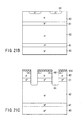
- a thermal oxide film (gate insulating film) 46 is formed to cover the surfaces of the p-type base layer 43, the emitter regions 44 and the trench 45, as shown in FIG. 13H. Further, a polysilicon layer (gate electrode) 47 doped with an n-type impurity is formed on the oxide film 46 such that the trench 45 is filled with the polysilicon layer 47.
- a patterning for forming a lead of the trench-gate electrode is applied to the polysilicon layer 47 based a trench-gate lead pattern so as to form a pad (not shown) for the gate electrode contact. Also, the polysilicon layer 47 is etched back to reach an opening portion of the trench 45.
- an insulating film 49 is formed on the surface of the oxide film 46 covering the p-type base layer 43 and the emitter region 44 and on the surface of the polysilicon layer 47 buried in the trench 45, as shown in FIG. 13J.
- a resist film is laminated on the surface of the insulating film 49, followed by forming a resist pattern 102 by the photolithography.
- the resist pattern 102 thus formed covers some portions of the surface of the p-type base layer 43 and the emitter region 44, which are positioned between the adjacent trenches 45, and is provided with band-like openings arranged in parallel to the trenches 45, as shown in FIG. 13K.
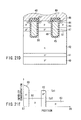
- the insulating film 49 and the oxide film 46 are etched with the resist pattern 102 used as a mask so as to expose the p-type base layer 43 and a part of the emitter region 44 to the outside.
- a pad (not shown) for the gate electrode contact is also exposed to the outside.
- an Al-Si (aluminum-silicon) film is formed on the entire surface, followed by patterning the Al-Si film so as to form an emitter electrode 48 in contact with both the p-type base layer 43 and the emitter region 44, which are exposed to the outside in the preceding etching treatment, and a gate electrode wiring (not shown) that is brought into contact with the pad for the gate electrode contact, as shown in FIG. 13L. Further, a collector electrode 50 is formed on the back surface of the p + -type silicon substrate 40.
- the trench IGBT constructed as shown in FIG. 3A described previously can be formed by the manufacturing method described above.
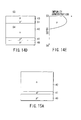
- FIGS. 14A, 14B and 14D are cross sectional views collectively showing the manufacturing process of the trench IGBT.
- FIGS. 14C and 14E are graphs showing the impurity concentration profiles in the depth direction along the lines S3-S4 shown in FIGS. 14B and 14D, respectively.
- an n + -type buffer layer 41 and an n - -type base layer 42 are formed by the epitaxial growth on a p + -type silicon substrate 40, as shown in FIG. 14A.
- a p-type impurity e.g., boron
- FIG. 14C shows the impurity concentration profile in the p-type base layer 104.
- FIG. 14E shows the impurity concentration profile in the p-type base layer 43 and the p + -type base layer 51.
- the manufacturing steps as in the first embodiment are followed in the subsequent steps so as to manufacture the trench IGBT as shown in FIG. 3A.
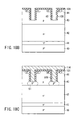
- FIGS. 15A to 15F are cross sectional views collectively showing the manufacturing process of a trench IGBT having a trench contact structure.
- an n + -type buffer layer 41 and an n - -type base layer 42 are formed by the epitaxial growth on a p + -type silicon substrate 40, as shown in FIG. 15A.
- a p-type impurity e.g., boron
- an n + -type emitter layer 44 is formed by using a mask 100 and, then, a trench 45 is formed by using a mask 101. Further, a thermal oxide film 46 is formed, and a polysilicon layer 47 doped with an n-type impurity is buried in the trench 45. Still further, the deposited polysilicon layer 47 is etched back to reach an opening portion of the trench 45, and a pad (not shown) for the gate electrode contact is formed, followed by laminating an insulating film 49. Then, the insulating film 49 and the oxide film 46 are patterned by etching, followed by forming an oxide film pattern 107 on the surface.
- a trench 52 having the bottom portion positioned in the intermediate portion of the p-type base layer 43 is formed by using the oxide film pattern 107 as a mask, and ions of a p-type impurity such as boron are implanted through the trench 52, followed by applying a thermal diffusion treatment so as to form a p + -type base layer 51, as shown in FIG. 15E.
- the time, temperature, etc. are controlled so as to form the p + -type base layer 51 in a manner to extend to reach the channel region CH.
- the oxide film pattern 107 is removed, followed by forming an Al-Si film on the entire surface and subsequently patterning the Al-Si film so as to form an emitter electrode 48 and a gate electrode wiring (not shown), as shown in FIG. 15F.
- the emitter electrode 48 is in contact with the upper surface of the emitter region 44 and with the p-type base layer 43 and the p + -type base layer 51 within the trench 52. Further, a collector electrode (not shown) is formed on the back surface of the p + -type silicon substrate 40.
- the trench 52 for the trench contact it was customary to form a trench only slightly deeper than the emitter layer 44. In this embodiment, however, formed is a trench considerably deeper than that in the prior art. In the trench contact, the degree of improvement in the short circuit withstand capability is increased with increase in the depth of the trench.
- the trench IGBT as shown in FIG. 6 can be manufactured by the manufacturing method described above.
- FIGS. 16A to 16F are cross sectional views collectively showing the manufacturing process of a trench IGBT having a trench contact.
- an n + -type buffer layer 41 and an n-type base layer 42 are formed on a p + -type silicon substrate 40 by epitaxial growth as shown in FIG. 16A.
- an n + -type emitter layer 44 and a trench 45 extending through the n + -type emitter layer 44 are formed, as shown in FIGS. 16B to 16C.
- a thermal oxide film 46 is formed to cover the side wall of the trench 45 and the upper surfaces of the n + -type emitter layer 44 and the n - -type base layer 42, followed by burying a polysilicon layer 47 doped with an n-type impurity in the trench 45.
- the polysilicon layer 47 is etched back to reach the open portion of the trench 45, and forms a pad (not shown) for the gate electrode contact, followed by forming an insulating film 49. Still further, the insulating film 49 and the oxide film 46 are patterned by etching, followed by forming an oxide pattern 107 on the surface.
- a trench 42 having the bottom positioned within the n - -type base layer 42 is formed by using the oxide pattern as a mask and, then, ions of a p-type impurity such as boron are implanted into the n - -type base layer 42 through the trench 52, as shown in FIG. 16D.
- a p-type base layer 43 is formed in the n - -type base layer 42 by thermal diffusion, as shown in FIG. 16E. Then, a p + -type base layer 51 is formed as shown in FIG. 16F by implanting ions of a p-type impurity such as boron into the p-type base layer 43 through the trench 52.
- a p-type impurity such as boron
- the oxide pattern 107 is removed, followed by forming an Al-Si layer and subsequently patterning the Al-Si layer so as to form an emitter electrode and a gate electrode wiring (not shown), which are in contact with the p-type base layer 43, the p + -type base layer 51 and the n + -type emitter region 44. Further, a collector electrode (not shown) is formed on the back surface of the p + -type silicon substrate 40.
- the trench IGBT constructed as shown in FIG. 7 can be manufactured by the manufacturing process described above.
- FIGS. 17A to 17D are cross sectional views collectively showing the process of manufacturing the trench IGBT.
- FIG. 17A is prepared by the steps shown in FIGS. 15A and 15B relating to the manufacturing method according to the third embodiment of the present invention.
- a pattern of an oxide film 101 is formed, followed by forming a trench 45 extending to reach an n - -type base layer 42 by using the pattern of the oxide film 101 as a mask and subsequently implanting ions of a p-type impurity such as boron into a bottom region of the trench 45, as shown in FIG. 17B.
- a p + -type base layer 51 is selectively formed in the surface region of the n - -type base layer 42 by thermal diffusion, as shown in FIG. 17C.
- the trench 45 is further deepened to extend through the p + -type base layer 51 so as to have the bottom of the trench 45 positioned within the n - -type base layer 42.
- the manufacture of the trench IGBT is completed by the steps shown in FIGS. 13H to 13L relating to the manufacturing process according to the first embodiment of the present invention.
- FIGS. 18A to 18D are cross sectional views collectively showing the manufacturing process of the trench IGBT.
- FIG. 18A is prepared by the steps shown in FIGS. 15A and 15B relating to the manufacturing method according to the third embodiment of the present invention.
- an oxide film pattern 101 is formed on an emitter layer 44 and a p-type base layer 43, followed by forming a trench 45 in a manner to have the bottom thereof positioned within the p-type base layer 43 by using the oxide film pattern 101 as a mask, as shown in FIG. 18B.
- an oxide film 109 is formed by oxidizing the side wall of the trench 45, followed by selectively removing the oxide film 109 positioned on the bottom of the trench 45 by, for example, RIE.
- a polysilicon layer 114 doped with a p-type impurity in a high concentration is buried in the trench 45, as shown in FIG. 18C, followed by applying a heat treatment.
- the p-type impurity is diffused from the polysilicon layer 114 into the p-type base layer 43 so as to form a p + -type base layer 51 having a high impurity concentration.
- the polysilicon layer 114 is removed by RIE, as shown in FIG. 18D. Then, the trench 45 having the bottom positioned within the p-type base layer 43 is deepened by RIE such that the bottom of the trench 45 is positioned within the n - -type base layer 42.
- the manufacture of the trench IGBT is completed by the steps shown in FIGS. 13H to 13L relating to the manufacturing process according to the first embodiment of the present invention.
- the trench IGBT as shown in FIG. 5 can be manufactured by the manufacturing method described above.
- FIGS. 19A to 19D are cross sectional views collectively showing the manufacturing process of the trench IGBT.
- FIG. 19A is prepared by the steps shown in FIGS. 16A and 16C relating to the manufacturing method according to the fourth embodiment of the present invention.
- a trench 45 is formed within a p-type base layer 52, followed by oxidizing the inner wall of the trench 52 so as to form an oxide film 109 and subsequently removing the oxide film 109 positioned on the bottom of the trench 52, as shown in FIG. 19B. Further, the oxide film pattern 107 is removed, followed by depositing a polysilicon layer 114 doped with a p-type impurity in a high concentration on the trench 52, the insulating film 49 and the emitter layer 44, as shown in FIG. 19C.
- the polysilicon layer 114 is removed by a dry etching method or a wet etching method, followed by forming simultaneously an emitter electrode 48 in contact with the p-type base layer 43, the p + -type base layer 51 and the n + -type emitter region 44 and a gate electrode wiring (not shown) in contact with the gate electrode 47. Also, a collector electrode is formed on the back surface of the p + -type silicon substrate 40 so as to finish manufacturing the trench IGBT.
- FIGS. 20A to 20D are cross sectional views collectively showing the manufacturing process of the trench IGBT.
- an n + -type buffer layer 41 and an n - -type base layer 42 are formed on a p + -type silicon substrate 40 by the epitaxial growth, as shown in FIG. 20A.
- a p + -type base layer 53 having a high impurity concentration and a uniform impurity concentration distribution, i.e., the distribution of the impurity concentration being substantially free from dependence on the location, is formed by the epitaxial growth on the n - -type base layer 42.
- ions of an n-type impurity such as phosphorus are implanted into the surface region of the p + -type base layer 53, followed by applying a heat treatment so as to diffuse the n-type impurity, thereby forming an n + -type emitter layer 44 in the surface region of the p + -type base layer 53, as shown in FIG. 20B.
- an oxide film 101 is formed as a shielding film on the n + -type emitter layer 44, followed by forming a trench 45 extending from the surface of the emitter layer 44 to reach the n - -type base layer 42 through the p + -type base layer 53, as shown in FIG. 20C. Then, the oxide film 101 is removed by etching.
- a gate insulating film 46, a trench-gate electrode 47, an insulating film 49, and an emitter electrode 48 are formed by the steps shown in FIGS. 13H to 13L, which are included in the manufacturing method according to the first embodiment of the present invention, followed by forming a collector electrode on the back surface of the p + -type silicon substrate 40, thereby completing the manufacture of a trench IGBT.
- the trench IGBT constructed as shown in FIG. 8A can be manufactured by the manufacturing method described above.
- FIGS. 21A to 21D are cross sectional views collectively showing the manufacturing process of the trench IGBT.
- an n + -type buffer layer 41 and an n - -type base layer 42 are formed on a p + -type silicon substrate 40 by the epitaxial growth, as shown in FIG. 21A.
- a p-type base layer 43 is formed on the p + -type base layer by the epitaxial growth method as shown in FIG. 21B. Ions of an n-type impurity such as phosphorus are implanted into the surface region of the p-type base layer 43, followed by applying a heat treatment so as to diffuse the n-type impurity and, thus, to form an n + -type emitter layer 44 in the surface region of the p-type base layer 43.
- an n-type impurity such as phosphorus
- an oxide film 101 acting as a shielding film is formed on the n + -type emitter layer 44, followed by forming a trench 45 extending from the surface of the emitter layer 44 to reach the n - -type base layer 42 through the p-type and p + -type base layers 43 and 51, as shown in FIG. 21C, and subsequently removing the oxide film 101 by etching.
- a gate insulating film 46, a trench-gate electrode 47, an insulating film 49, and an emitter electrode 48 are formed by the steps shown in FIGS. 13H to 13L, which are included in the manufacturing method according to the first embodiment of the present invention, followed by forming a collector electrode on the back surface of the p + -type silicon substrate 40, thereby completing the manufacture of a trench IGBT.
- FIG. 21E is a graph showing the impurity concentration profile along the line S7-S8 shown in FIG. 21, which covers the region ranging between the n + -type base region 44 and the n - -type base layer 42. As apparent from the graph of FIG. 21E, it is possible to form the impurity concentration distribution in the p-type base layer such that the highest impurity concentration is formed in the junction with the n - -type base layer in the manufacturing method according to the ninth embodiment of the present invention.
- FIGS. 22A, 22B, 22D and 22E are cross sectional views collectively showing the manufacturing process of the trench IGBT.
- FIGS. 22C and 22F are graphs showing the impurity concentration profiles in the depth direction along the lines S5-S6 shown in FIGS. 22B and 22E, respectively.
- an n + -type buffer layer 41 and an n - -type base layer 42 are formed on a p + -type silicon substrate 40 by the epitaxial growth, as shown in FIG. 22A.
- ions of a p-type impurity such as boron are implanted with a low dose into the surface region of the n - -type base layer 42, followed by performing a thermal diffusion so as to form a p-type base layer 43 in the surface region of the n - -type base layer 42, as shown FIG. 22B.
- FIG. 22C shows an impurity concentration profile along the line S5-S6 shown in FIG. 22B, which covers the region ranging between the p-type base region 43 and the n - -type base layer 42.
- the impurity concentration profile shown in FIG. 22C includes the p-type impurity concentration distribution 61 in the p-type base layer 43, and the n-type impurity concentration distribution 63 in the n - -type base layer 42.
- the mark "Cp2" shown in FIG. 22C represents the highest p-type impurity concentration in the p-type base layer 43.
- ions of a p-type impurity such as boron are implanted into the surface region of the p-type base layer 43 at a dose that permits the MOSFET to exhibit a desired threshold value, as shown in FIG. 22D, followed by performing a thermal diffusion.
- a p + -type base layer 51 is formed within the p-type base layer 43, as shown in FIG. 22F.
- FIG. 22F shows an impurity concentration profile along the line S5-S6 shown in FIG. 22E, which covers the region ranging between the p-type base region 43 and the n - -type base layer 42.
- the impurity concentration profile shown in FIG. 22F includes the p-type impurity concentration distribution 61 in the p-type base layer 43, the p-type impurity concentration distribution 62 in the p + -type base layer 51, and the n-type impurity concentration distribution 63 in the n - -type base layer 42.
- the 22F represent the highest p-type impurity concentrations in the p-type base layer 43 and the p + -type base layer 51, respectively.
- the highest concentration Cp1 of the p-type impurity in the p-type base regions (43, 51) is formed in the vicinity of the junction between the p + -type base layer 43 and the n - -type base region.
- the accelerating energy in the second ion implantation is determined to permit the conductance g1 between the point Cp1 and the surface of the p-type base layer 43 to be not larger than the conductance g2 between the junction between the p-type base layer 43 and the n - -type base layer 42 and the point Cp1.
- the present inventors have found that it is possible to obtain a desired short circuit withstand capability by setting the peak Cp1 of the impurity concentration distribution in the p + -type base layer 51 in a depth of at least 1 ⁇ m from the surface of the p-type base layer 43.
- ions of a p-type impurity such as boron should be implanted under an accelerating energy of at least 500 keV.
- an n + -type emitter layer, a trench, a gate insulating film, a trench-gate electrode, an insulating film, and an emitter electrode are formed by the steps shown in FIGS. 13F to 13K, which are included in the manufacturing method according to the first embodiment of the present invention, followed by forming a collector electrode on the back surface of the p + -type silicon substrate 40, thereby completing the manufacture of a trench IGBT.
- the manufacturing method of an IGBT according to any of the first to tenth embodiments described above can also be applied to the manufacture of a power MOSFET.
- the saturation current value can be decreased in the present invention by controlling the pinch-off point in the channel region, making it possible to improve the short circuit withstand capability of the power semiconductor element.
Landscapes
- Insulated Gate Type Field-Effect Transistor (AREA)
- Thyristors (AREA)
- Thin Film Transistor (AREA)
- Metal-Oxide And Bipolar Metal-Oxide Semiconductor Integrated Circuits (AREA)
- Electrodes Of Semiconductors (AREA)
Abstract
Description
| Concentration peak position within p-type base layer [µm] | 0 | 0.5 | 1 | 1.5 | 2 |
| Saturated current of IGBT [A] | 2500 | 2300 | 1400 | 1300 | 1100 |
| Short circuit withstand capability [µs] | ≦ 1 | ≦ 1 | 12 | 15 | 17 |
| Accelerating voltage [keV] | 60 | 100 | 300 | 500 | 600 |
| Short circuit withstand capability [µs] | 0 | 6 | 11 | 14 | 15.5 |
Claims (28)
- A semiconductor element, comprising a first base layer of a first conductivity type; a second base layer of a second conductivity type formed selectively in one surface region of said first base layer; an emitter layer or a source layer of the first conductivity type formed selectively in a surface region of said second base layer; a gate electrode formed on that portion of said second base layer which is positioned between said emitter layer or source layer and said first base layer with a gate insulating film interposed between said gate electrode and said second base layer; a collector layer or a drain layer formed on the other surface region of said first base layer or formed selectively on one surface region of the first base layer; a first main electrode formed on said collector layer or on said drain layer; a second main electrode formed on said emitter layer or source layer and on said second base layer; and a channel region formed in contact with said gate insulating film to permit the carrier to migrate between the emitter layer or source layer and the first base layer, characterized in that said channel region has an impurity concentration profile such that the impurity concentration that permits bringing about a pinch-off phenomenon most promptly within said channel is formed in a position closer to the first base layer (42, 71) than to the junction between the emitter layer (44) or source layer (73) and the second base layer (43, 72).
- The semiconductor element according to claim 1, characterized in that the impurity concentration causing said pinch-off phenomenon in a position close to said first base layer (42, 71) is equal to the highest concentration in said impurity concentration profile of said channel region.
- The semiconductor element according to claim 1, characterized in that the impurity concentration profile in said channel region has, in a region between the junction portion with said emitter layer (44) or source layer (73) and a point of the highest impurity concentration, an impurity concentration gradient lower than that in said junction portion, the impurity concentration gradient in said junction portion being formed by the overlapping of the impurity concentration profile in said second base layer (43, 72) with the impurity concentration profile in said emitter layer (44) or source layer (73).
- The semiconductor element according to claim 1, characterized in that, in said channel region, the channel conductance between said first base layer (42, 51) and a point of the highest impurity concentration in said second base layer (43, 51, 72, 80) is higher than the channel conductance between said emitter layer (44) or source layer (73) and a point of the highest impurity concentration in said second base layer (43, 51, 72, 80).
- The semiconductor element according to claim 1, characterized in that said second main electrode (48, 77) is formed on the bottom surface and/or the side surface of a groove (52) formed to extend downward to reach an intermediate portion of said second base layer (43, 51, 72, 80).
- A semiconductor element, comprising a first base layer of a first conductivity type; a second base layer of a second conductivity type formed selectively in one surface region of said first base layer; an emitter layer or a source layer of the first conductivity type formed selectively in a surface region of said second base layer; a gate electrode formed on that portion of said second base layer which is positioned between said emitter layer or source layer and said first base layer with a gate insulating film interposed between said gate electrode and said second base layer; a collector layer or a drain layer formed on the other surface region of said first base layer or formed selectively on one surface region of the first base layer; a first main electrode formed on said collector layer or on said drain layer; and a second main electrode formed on said emitter layer or source layer and on said second base layer; characterized in that a third base layer (51, 80) is formed within said second base layer (43, 72) so as to be isolated from said emitter layer (44) or source layer (73) and is formed in contact with said gate insulating film (46, 75), the point of the highest impurity concentration of a first impurity concentration profile along the gate insulating film (46, 75) within said third base layer (51, 80) and in the direction in which said emitter layer (44) or source layer (73), the second base layer (43, 72), and the first base layer (42, 71) are arranged in the order mentioned being positioned closer to the first base layer (42, 71) than the point of the highest impurity concentration of a second impurity concentration profile along the gate insulating film (46, 75) within said second base layer (43, 72) and in the direction in which the emitter layer (44) or source layer (73), the second base layer (43, 72) and the first base layer (42, 71) are arranged in the order mentioned.
- The semiconductor element according to claim 6, characterized in that the highest impurity concentration of said first impurity concentration profile within said third base layer (51, 80) is not lower than the highest impurity concentration of said second impurity concentration profile within said second base layer (43, 72).
- The semiconductor element according to claim 6, characterized in that a third impurity concentration profile, which results from the overlapping of said first and second impurity concentration profiles, has an impurity concentration gradient smaller than the impurity concentration gradient at the junction with said emitter layer (44) or said source layer (73) in the position between said junction and the position of the highest impurity concentration, the impurity concentration gradient in said junction being formed by the overlapping between said second impurity concentration profile and a fourth impurity concentration profile in said emitter layer (44) or source layer (73).
- The semiconductor element according to claim 6, characterized in that, in said second and third base layers (43, 51, 72, 80), the channel conductance between said first base layer (42, 71) and the point of the highest impurity concentration within said third base layer (51, 80) is higher than the channel conductance between said emitter layer (44) or source layer (73) and the position of the highest impurity concentration within said third base layer (51, 80).
- The semiconductor element according to claim 6, characterized in that said third base layer (51, 80) is in contact with said first base layer (42, 71).
- The semiconductor element according to claim 6, characterized in that the region of the highest impurity concentration in said third base layer (51, 80) is selectively formed at the interface between said second base layer (43, 72) and said gate insulating film (46, 75) and in the vicinity of said interface.
- The semiconductor element according to claim 6, characterized in that said second main electrode (48, 77) is formed on the bottom surface and/or side surface of a groove (52) formed to extend through said second base layer (43, 72) to reach an intermediate depth of said third base layer (51, 80) and is in contact with said third base layer (51, 80) on the bottom surface and/or the side surface of said groove (52).
- A semiconductor element, comprising a first base layer of a first conductivity type; a second base layer of a second conductivity type formed selectively in one surface region of said first base layer; an emitter layer or a source layer of the first conductivity type formed selectively in a surface region of said second base layer; a gate electrode formed on that portion of said second base layer which is positioned between said emitter layer or source layer and said first base layer with a gate insulating film interposed between said gate electrode and said second base layer; a collector layer or a drain layer formed on the other surface region of said first base layer or formed selectively on one surface region of the first base layer; a first main electrode formed on said collector layer or on said drain layer; a second main electrode formed on said emitter layer or source layer and on said second base layer; and a channel region formed in contact with said gate insulating film to permit the carrier to migrate between said emitter layer or source layer and said first base layer, characterized in that said channel region has an impurity concentration profile such that the impurity concentration is substantially constant along said gate insulating film (46, 75) and in the direction in which the emitter layer (44) or source layer (73), the second base layer (43, 72), and the first base layer (42, 71) are formed in the order mentioned.
- The semiconductor element according to any one of claims 1, 6 and 13, characterized in that said gate electrode (47, 76) is buried in a trench (45, 74) with a gate insulating film (46, 75) interposed between said gate electrode and said trench, said trench (45, 74) being formed to extend from the surface of said emitter layer (44) or source layer (73) to reach an intermediate portion of said first base layer (42, 71) through said second base layer (53, 72).
- The semiconductor element according to any one of claims 1, 6 and 13, characterized in that said gate electrode (47, 76) is formed on said gate insulating film (46, 75) formed on the surface of said second base layer (53, 72).
- A method of fabricating a semiconductor element, comprising the steps of selectively forming a second base layer of a second conductivity type in one surface region of a first base layer of a first conductivity type; selectively forming an emitter layer or source layer of the first conductivity type in a surface region of said second base layer; forming a gate electrode on the surface of that region of said second base layer which is positioned between said emitter layer or source layer and said first base layer with a gate insulating film interposed between said gate electrode and said second base layer; selectively forming a collector layer or drain layer in the other surface region of said first base layer or in one surface region of said first base layer; and forming a first main electrode in contact with said collector layer or drain layer and a second main electrode in contact with said emitter layer or source layer and said second base layer, characterized in that said second base layer (43, 51, 72, 80) is formed to have an impurity concentration profile such that the peak of the concentration is positioned closer to the junction with said first base layer (42, 71) in the step of forming said second base layer (43, 51, 72, 80).
- The method of fabricating a semiconductor element according to claim 16, characterized in that said step of forming said second base layer (43, 51, 72, 80) includes the sub-steps of:forming a third base layer (103) of the second conductivity type by selectively implanting ions of an impurity of the second conductivity type into a surface region of said first base layer (42, 71), followed by thermally diffusing the implanted impurity ions; andimplanting ions of an impurity of the first conductivity type into a surface region of said third base layer (103), followed by thermally diffusing the implanted impurity ions, thereby lowering the concentration of the impurity of the second conductivity type in the surface region of said third base layer (103) so as to form a fourth base layer (43, 72) of the second conductivity type.
- The method of fabricating a semiconductor element according to claim 16, characterized in that said step of forming said second base layer (43, 51, 72, 80) includes the sub-steps of:selectively implanting ions of an impurity of the second conductivity type into a surface region of said first base layer (42, 71), followed by thermally diffusing the implanted ions so as to form a third base layer (104) of the second conductivity type; andapplying heat to said third base layer (104) so as to diffuse outward the impurity of the second conductivity type in the vicinity of the surface of said third base layer (104), thereby lowering the concentration of the impurity of the second conductivity type in the vicinity of the third base layer (104) so as to form a fourth base layer (43, 72) of the second conductivity type.
- The method of fabricating a semiconductor element according to claim 16, characterized in that said step of forming said second base layer (43, 51, 72, 80) includes the sub-steps of:forming a third base layer (43, 72) of the second conductivity type by implanting ions of an impurity of the second conductivity type into a surface region of said first base layer (42, 71) at a first dose and under a first accelerating energy;forming a fourth base layer (51, 80) of the second conductivity type in said third base layer (43, 72), the impurity concentration in said fourth base layer (51, 80) being higher than that in said third base layer (43, 72), by implanting ions of an impurity of the second conductivity type into said third base layer (43, 72) at a second dose higher than said first dose and under a second accelerating energy higher than said first accelerating energy; andthermally diffusing the implanted ions of the second conductivity type.
- The method of fabricating a semiconductor element according to any one of claims 16 to 19, characterized in that said step of forming said gate electrode (47, 76) includes the sub-steps of:forming a trench (45) extending from the surface of said emitter layer (44) or source layer to reach an intermediate depth of said first base layer (42, 71) through said second base layer (43, 51, 72, 80);forming a gate insulating film (46, 75) on the bottom and side wall of said trench (45, 74); andburying a gate electrode (47, 76) in said trench (45, 74).
- A method of fabricating a semiconductor element, comprising the steps of selectively forming a second base layer of a second conductivity type in one surface region of a first base layer of a first conductivity type; selectively forming an emitter layer or source layer of the first conductivity type in a surface region of said second base layer; forming a gate electrode on the surface of that region of said second base layer which is positioned between said emitter layer or source layer and said first base layer with a gate insulating film interposed between said gate electrode and said second base layer; selectively forming a collector layer or drain layer in the other surface region of said first base layer or in one surface region of said first base layer; and forming a first main electrode in contact with said collector layer or drain layer and a second main electrode in contact with said emitter layer or source layer and said second base layer, characterized by comprising the step of forming a third base layer (51, 80) of the second conductivity type, which is isolated from said emitter layer (44) or source layer (73), within said second base layer (43, 72) after or simultaneously with the step of forming said gate electrode (47, 76).
- The method of fabricating a semiconductor element according to claim 21,
characterized in that said step of forming said third base layer (51, 80) includes the sub-steps of:forming said gate electrode (47, 76), followed by forming a groove (52) having the bottom positioned within said second base layer (43, 72); andimplanting ions of an impurity of the second conductivity type into a region in the vicinity of the bottom portion of said groove (52), followed by thermally diffusing the implanted ions so as to form a third base layer (51, 80) of the second conductivity type at least in contact with said gate insulating film, the position of the highest concentration of the impurity concentration distribution within said third base layer (51, 80) being closer to said first base layer (42, 71) than the position of the highest concentration of the impurity concentration distribution within said second base layer (43, 72); andwherein said second main electrode (48, 77) is formed in contact with said second and third base layers (43, 51, 72, 80) and said emitter layer (44) or source layer (73) on the bottom surface and/or side surface of said groove (52) in the step of forming said second main electrode (48, 77). - The method of fabricating a semiconductor element according to claim 21, characterized in that said step of forming said gate electrode (47, 76) and said third base layer (51, 80) includes the sub-steps of:forming a trench (45, 74) extending through said emitter layer (44) or source layer (73) to reach said first base layer (42, 71);forming a third base layer (51, 80) by implanting ions of an impurity of the second conductivity type into a region in the vicinity of the bottom of said trench (45, 72), followed by thermally diffusing said impurity;deepening said trench (45, 74) to reach an intermediate depth of said first base layer (42, 71);forming said gate insulating film (46, 75) on the bottom and side surface of said trench (45, 74); andburying said gate electrode (47, 76) in said trench (45, 74).
- The method of fabricating a semiconductor element according to claim 21, characterized in that said step of forming said gate electrode (47, 76) and said third base layer (51, 80) includes the sub-steps of:forming a trench (45, 74) extending through said emitter layer (44) or source layer (73) and having the bottom positioned within said second base layer (43, 72);forming a masking material layer (109) on the side wall of said trench (45, 74);burying a diffusion source (114) containing an impurity of the second conductivity type in said trench (45, 74);forming a third base layer (51, 80) of the second conductivity type by applying heat to said diffusion source (114) so as to diffuse the impurity of the second conductivity type contained in said diffusion source (114) into a region in the vicinity of the bottom of said trench (45, 74);removing the diffusion source (114) positioned within the trench (45, 74);deepening the trench (45, 74) to reach an intermediate depth of said first base layer (43, 71);forming a gate insulating film (46, 75) on the bottom and side surface of the trench (45, 74); andburying said gate electrode (47, 76) in the trench (45, 74).
- The method of fabricating a semiconductor element according to claim 21,
characterized in that said step of forming said third base layer (51, 80) includes the sub-steps of:forming a gate electrode (47, 76), followed by forming a groove (52) having the bottom positioned within said second base layer (43, 72);forming a masking material layer (109) on the side wall of said groove (52);burying a diffusion source (114) containing an impurity of the second conductivity type in said groove (52);forming a third base layer (51, 80) of the second conductivity type by applying heat to said diffusion source (114) so as to diffuse the impurity of the second conductivity type contained in said diffusion source (114) into a region in the vicinity of the bottom of said groove (52); andremoving said diffusion source (114) positioned within said groove (52);wherein said second main electrode (48, 77) is formed in contact with said second and third base layers (43, 51, 72, 80) and with said emitter layer (44) or source layer (73) on the bottom and/or side surface of said groove (52) in the step of forming said second main electrode (48, 77). - A method of fabricating a semiconductor element, comprising the steps of selectively forming an emitter layer or source layer of a first conductivity type in one surface region of a first base layer of the first conductivity type; forming a trench extending through said emitter layer or source layer and having the bottom portion positioned within said first base layer; forming a gate insulating film to cover the bottom and the side surface of said trench; forming a gate electrode on said gate insulating film; forming a groove having a bottom positioned within said first base layer; forming a second base layer of the second conductivity type in a surface region of said first base layer such that said second base layer is in contact with said gate insulating film by introducing an impurity of the second conductivity type into said first base layer in the bottom and in the vicinity of the side wall of said groove, followed by applying a thermal diffusion to the introduced impurity; selectively forming a collector layer or drain layer in the other surface region of said first base layer; and forming a first main electrode in contact with said collector layer or drain layer and a second main electrode in contact with said emitter layer or source layer, and said second base layer, said second main electrode being in contact with said second base layer and said emitter layer or source layer in the side wall of said groove, characterized by further comprising the step of forming a third base layer (51, 80) of the second conductivity type in contact with said gate insulating film (46, 75) by further implanting ions of an impurity of the second conductivity type into said second base layer (42, 72) in the vicinity of the bottom of said groove (52) after the step of forming said second base layer (42, 72), followed by thermally diffusing said implanted impurity, said third base layer being contact with said second main electrode in the bottom and/or the side wall of said groove.
- A method of fabricating a semiconductor element, comprising the steps of forming a second base layer of a second conductivity type in one surface region of a first base layer of a first conductivity type; selectively forming an emitter layer or source layer of the first conductivity type in a surface region of said second base layer; forming a gate electrode on the surface of that region of said second base layer which is positioned between said emitter layer or source layer and said first base layer with a gate insulating film interposed between said gate electrode and said second base layer; selectively forming a collector layer or drain layer on the other surface region of said first base layer or on one surface region of said first base layer; and forming a first main electrode in contact with said collector layer or drain layer and a second main electrode in contact with said emitter layer or source layer and said second base layer, characterized in that said step of forming the second base layer (52) is carried out by an epitaxial growth such that the impurity concentration is rendered constant in the depth direction.
- The method of fabricating a semiconductor element according to claim 27,
characterized in that said step of forming said second base layer (53) includes the sub-steps of:forming a third base layer (51, 80) of the second conductivity type on said first base layer (42, 71) such that the impurity concentration in the depth direction is set constant at a first concentration; andforming a fourth base layer (43, 72) of the second conductivity type on said third base layer (51, 80) such that the impurity concentration in the depth direction is set constant at a second concentration higher than said first concentration;wherein said emitter layer (44) or source layer (73) is formed in said fourth base layer (43).
Applications Claiming Priority (2)
| Application Number | Priority Date | Filing Date | Title |
|---|---|---|---|
| JP2000060480A JP4371521B2 (en) | 2000-03-06 | 2000-03-06 | Power semiconductor device and manufacturing method thereof |
| JP2000060480 | 2000-03-06 |
Publications (2)
| Publication Number | Publication Date |
|---|---|
| EP1132970A2 true EP1132970A2 (en) | 2001-09-12 |
| EP1132970A3 EP1132970A3 (en) | 2008-02-20 |
Family
ID=18580789
Family Applications (1)
| Application Number | Title | Priority Date | Filing Date |
|---|---|---|---|
| EP01104596A Withdrawn EP1132970A3 (en) | 2000-03-06 | 2001-03-06 | Power semiconductor element capable of improving short circuit withstand capability while maintaining low on-voltage and method of fabricating the same |
Country Status (3)
| Country | Link |
|---|---|
| US (4) | US6495871B2 (en) |
| EP (1) | EP1132970A3 (en) |
| JP (1) | JP4371521B2 (en) |
Cited By (7)
| Publication number | Priority date | Publication date | Assignee | Title |
|---|---|---|---|---|
| EP2672516A4 (en) * | 2011-02-01 | 2014-08-06 | Sumitomo Electric Industries | SEMICONDUCTOR DEVICE |
| EP2637212A4 (en) * | 2010-11-01 | 2014-08-06 | Sumitomo Electric Industries | SEMICONDUCTOR DEVICE AND METHOD FOR MANUFACTURING THE SAME |
| WO2017193321A1 (en) * | 2016-05-12 | 2017-11-16 | 中山港科半导体科技有限公司 | Insulated gate bipolar transistor structure |
| CN109417093A (en) * | 2017-01-17 | 2019-03-01 | 富士电机株式会社 | semiconductor device |
| EP2293336B1 (en) * | 2008-05-20 | 2019-11-27 | Rohm Co., Ltd. | Semiconductor device |
| WO2021071758A1 (en) * | 2019-10-10 | 2021-04-15 | Cree, Inc. | Semiconductor device with improved short circuit withstand time and methods for manufacturing the same |
| WO2023285557A1 (en) * | 2021-07-16 | 2023-01-19 | Hitachi Energy Switzerland Ag | Production method and power semiconductor device |
Families Citing this family (82)
| Publication number | Priority date | Publication date | Assignee | Title |
|---|---|---|---|---|
| JP2002305304A (en) * | 2001-04-05 | 2002-10-18 | Toshiba Corp | Power semiconductor device |
| DE10117801B4 (en) * | 2001-04-10 | 2005-12-22 | Robert Bosch Gmbh | Semiconductor power device and corresponding manufacturing method |
| US7736976B2 (en) | 2001-10-04 | 2010-06-15 | Vishay General Semiconductor Llc | Method for fabricating a power semiconductor device having a voltage sustaining layer with a terraced trench facilitating formation of floating islands |
| US6465304B1 (en) | 2001-10-04 | 2002-10-15 | General Semiconductor, Inc. | Method for fabricating a power semiconductor device having a floating island voltage sustaining layer |
| US6576516B1 (en) * | 2001-12-31 | 2003-06-10 | General Semiconductor, Inc. | High voltage power MOSFET having a voltage sustaining region that includes doped columns formed by trench etching and diffusion from regions of oppositely doped polysilicon |
| US6566201B1 (en) | 2001-12-31 | 2003-05-20 | General Semiconductor, Inc. | Method for fabricating a high voltage power MOSFET having a voltage sustaining region that includes doped columns formed by rapid diffusion |
| US6750104B2 (en) * | 2001-12-31 | 2004-06-15 | General Semiconductor, Inc. | High voltage power MOSFET having a voltage sustaining region that includes doped columns formed by trench etching using an etchant gas that is also a doping source |
| US6656797B2 (en) | 2001-12-31 | 2003-12-02 | General Semiconductor, Inc. | High voltage power MOSFET having a voltage sustaining region that includes doped columns formed by trench etching and ion implantation |
| US6686244B2 (en) | 2002-03-21 | 2004-02-03 | General Semiconductor, Inc. | Power semiconductor device having a voltage sustaining region that includes doped columns formed with a single ion implantation step |
| JP4004843B2 (en) | 2002-04-24 | 2007-11-07 | Necエレクトロニクス株式会社 | Method for manufacturing vertical MOSFET |
| JP2004022941A (en) | 2002-06-19 | 2004-01-22 | Toshiba Corp | Semiconductor device |
| JP4892172B2 (en) * | 2003-08-04 | 2012-03-07 | ルネサスエレクトロニクス株式会社 | Semiconductor device and manufacturing method thereof |
| US7372088B2 (en) * | 2004-01-27 | 2008-05-13 | Matsushita Electric Industrial Co., Ltd. | Vertical gate semiconductor device and method for fabricating the same |
| JP4091921B2 (en) * | 2004-02-16 | 2008-05-28 | 松下電器産業株式会社 | Semiconductor device and manufacturing method thereof |
| JP2005340626A (en) * | 2004-05-28 | 2005-12-08 | Toshiba Corp | Semiconductor device |
| JP4575713B2 (en) * | 2004-05-31 | 2010-11-04 | 三菱電機株式会社 | Insulated gate semiconductor device |
| JP4703138B2 (en) * | 2004-06-18 | 2011-06-15 | 株式会社東芝 | Insulated gate semiconductor device |
| US7180159B2 (en) * | 2004-07-13 | 2007-02-20 | Texas Instruments Incorporated | Bipolar transistor having base over buried insulating and polycrystalline regions |
| DE102005040624A1 (en) * | 2004-09-02 | 2006-03-09 | Fuji Electric Holdings Co., Ltd., Kawasaki | Semiconductor component and method for its production |
| DE102004042758B4 (en) * | 2004-09-03 | 2006-08-24 | Infineon Technologies Ag | Semiconductor device |
| JP2006080177A (en) * | 2004-09-08 | 2006-03-23 | Sanyo Electric Co Ltd | Semiconductor device and manufacturing method thereof |
| JP2006120789A (en) * | 2004-10-20 | 2006-05-11 | Toshiba Corp | Semiconductor device |
| JP4440188B2 (en) * | 2005-01-19 | 2010-03-24 | パナソニック株式会社 | Manufacturing method of semiconductor device |
| US7686163B2 (en) * | 2005-05-09 | 2010-03-30 | Jimmy Cheuk Tsang | Ergonomic golf bag handle |
| US8188539B2 (en) * | 2005-08-10 | 2012-05-29 | Freescale Semiconductor, Inc. | Field-effect semiconductor device and method of forming the same |
| JP4939012B2 (en) * | 2005-08-26 | 2012-05-23 | ルネサスエレクトロニクス株式会社 | Semiconductor device |
| JP2007115943A (en) * | 2005-10-21 | 2007-05-10 | Toyota Central Res & Dev Lab Inc | Semiconductor device |
| JP2007129085A (en) * | 2005-11-04 | 2007-05-24 | Texas Instr Japan Ltd | Semiconductor device and manufacturing method thereof |
| JP5034461B2 (en) * | 2006-01-10 | 2012-09-26 | 株式会社デンソー | Semiconductor device |
| CN101366105B (en) * | 2006-02-07 | 2012-05-09 | 三菱电机株式会社 | Semiconductor device and method for manufacturing same |
| EP1852916A1 (en) * | 2006-05-05 | 2007-11-07 | Austriamicrosystems AG | High voltage transistor |
| US7666750B2 (en) * | 2006-09-13 | 2010-02-23 | Agere Systems Inc. | Bipolar device having improved capacitance |
| JP4561734B2 (en) * | 2006-12-13 | 2010-10-13 | 株式会社日立製作所 | Semiconductor device and plasma display device using the same |
| KR100890256B1 (en) * | 2007-05-29 | 2009-03-24 | 삼성전자주식회사 | Semiconductor device employing transistor having recess channel region and manufacturing method thereof |
| JP4492735B2 (en) * | 2007-06-20 | 2010-06-30 | 株式会社デンソー | Semiconductor device and manufacturing method of semiconductor device |
| JP5298488B2 (en) | 2007-09-28 | 2013-09-25 | 富士電機株式会社 | Semiconductor device |
| US7880200B2 (en) * | 2007-09-28 | 2011-02-01 | Infineon Technologies Austria Ag | Semiconductor device including a free wheeling diode |
| WO2009122486A1 (en) * | 2008-03-31 | 2009-10-08 | 三菱電機株式会社 | Semiconductor device |
| US7977768B2 (en) * | 2008-04-01 | 2011-07-12 | Infineon Technologies Ag | Semiconductor devices and methods of manufacture thereof |
| JP4840482B2 (en) * | 2008-10-14 | 2011-12-21 | 株式会社デンソー | Semiconductor device |
| JP2010098189A (en) * | 2008-10-17 | 2010-04-30 | Toshiba Corp | Semiconductor device |
| JP4929304B2 (en) | 2009-03-13 | 2012-05-09 | 株式会社東芝 | Semiconductor device |
| JP5013436B2 (en) | 2009-06-04 | 2012-08-29 | 三菱電機株式会社 | Power semiconductor device |
| US8164162B2 (en) * | 2009-06-11 | 2012-04-24 | Force Mos Technology Co., Ltd. | Power semiconductor devices integrated with clamp diodes sharing same gate metal pad |
| JP5361808B2 (en) | 2010-06-23 | 2013-12-04 | 三菱電機株式会社 | Power semiconductor device |
| JP2012064849A (en) * | 2010-09-17 | 2012-03-29 | Toshiba Corp | Semiconductor device |
| US9105495B2 (en) | 2011-02-12 | 2015-08-11 | Freescale Semiconductor, Inc. | Semiconductor device and related fabrication methods |
| JP2012248760A (en) * | 2011-05-30 | 2012-12-13 | Shindengen Electric Mfg Co Ltd | Trench gate power semiconductor device and manufacturing method of the same |
| JP6006918B2 (en) * | 2011-06-06 | 2016-10-12 | ルネサスエレクトロニクス株式会社 | SEMICONDUCTOR DEVICE, SEMICONDUCTOR DEVICE MANUFACTURING METHOD, AND ELECTRONIC DEVICE |
| CN103021856A (en) * | 2011-09-28 | 2013-04-03 | 比亚迪股份有限公司 | Method for forming semiconductor structure with super junctions and semiconductor structure |
| CN103094324B (en) * | 2011-11-08 | 2016-03-23 | 无锡华润上华半导体有限公司 | Trench-type insulated gate bipolar transistor and preparation method thereof |
| JP2013211512A (en) * | 2012-02-27 | 2013-10-10 | Toshiba Corp | Insulated-gate bipolar transistor |
| US20150123165A1 (en) * | 2012-05-30 | 2015-05-07 | Kyushu Institute Of Technology | High-voltage insulated gate type power semiconductor device and method of manufacturing the same |
| US8735937B2 (en) * | 2012-05-31 | 2014-05-27 | Taiwan Semiconductor Manufacturing Company, Ltd. | Fully isolated LIGBT and methods for forming the same |
| US9219144B2 (en) * | 2012-08-10 | 2015-12-22 | Infineon Technologies Austria Ag | Semiconductor device including a trench in a semiconductor substrate and method of manufacturing a semiconductor device |
| KR101876579B1 (en) * | 2012-09-13 | 2018-07-10 | 매그나칩 반도체 유한회사 | Power Semiconductor and Fabricating Method Thereof |
| JP2014060336A (en) | 2012-09-19 | 2014-04-03 | Toshiba Corp | Semiconductor device |
| JP5831526B2 (en) | 2013-01-17 | 2015-12-09 | 株式会社デンソー | Semiconductor device and manufacturing method thereof |
| CN103973277B (en) | 2013-02-05 | 2017-06-09 | 通用电气公司 | The short-circuit protection circuit and method of insulated gate bipolar transistor |
| US9142657B2 (en) * | 2013-03-15 | 2015-09-22 | David Schie | Gated thyristor power device |
| JP6077385B2 (en) * | 2013-05-17 | 2017-02-08 | トヨタ自動車株式会社 | Semiconductor device |
| JP6048317B2 (en) | 2013-06-05 | 2016-12-21 | 株式会社デンソー | Silicon carbide semiconductor device |
| CN104299989B (en) * | 2013-07-19 | 2018-06-12 | 无锡华润上华科技有限公司 | Insulated gate bipolar transistor and its manufacturing method |
| CN104795328B (en) * | 2014-01-16 | 2017-11-21 | 北大方正集团有限公司 | A kind of groove-shaped VDMOS manufacture methods and a kind of groove-shaped VDMOS |
| JP6279927B2 (en) * | 2014-02-17 | 2018-02-14 | トヨタ自動車株式会社 | Method for manufacturing insulated gate type switching element and insulated gate type switching element |
| TWI518751B (en) * | 2014-05-14 | 2016-01-21 | 國立清華大學 | A carrier channel with gradient distributing element concentration |
| US9391184B2 (en) * | 2014-05-27 | 2016-07-12 | Pakal Technologies, Llc | Insulated gate turn-off device with turn-off transistor |
| JP2016034001A (en) * | 2014-07-31 | 2016-03-10 | トヨタ自動車株式会社 | Semiconductor device and method of manufacturing the same |
| JP6115678B1 (en) | 2016-02-01 | 2017-04-19 | 富士電機株式会社 | Silicon carbide semiconductor device and method for manufacturing silicon carbide semiconductor device |
| DE102016226237B4 (en) | 2016-02-01 | 2024-07-18 | Fuji Electric Co., Ltd. | SILICON CARBIDE SEMICONDUCTOR DEVICE |
| US9935188B2 (en) * | 2016-07-22 | 2018-04-03 | Pakal Technologies Llc | Insulated gate turn-off device with turn-off Schottky-Barrier MOSFET |
| JP2018207057A (en) * | 2017-06-09 | 2018-12-27 | ルネサスエレクトロニクス株式会社 | Semiconductor device and method for manufacturing the same |
| JP7139683B2 (en) * | 2018-05-17 | 2022-09-21 | 富士電機株式会社 | Semiconductor integrated circuit and its manufacturing method |
| JP7184090B2 (en) * | 2018-10-10 | 2022-12-06 | サンケン電気株式会社 | Semiconductor device and its manufacturing method |
| JP7085975B2 (en) | 2018-12-17 | 2022-06-17 | 三菱電機株式会社 | Semiconductor device |
| CN111370476B (en) * | 2018-12-25 | 2022-03-29 | 上海睿驱微电子科技有限公司 | IEGT with hole current carrying path and method of construction thereof |
| US11158703B2 (en) * | 2019-06-05 | 2021-10-26 | Microchip Technology Inc. | Space efficient high-voltage termination and process for fabricating same |
| JP7278913B2 (en) | 2019-09-13 | 2023-05-22 | 株式会社東芝 | Semiconductor device, method for manufacturing semiconductor device, inverter circuit, drive device, vehicle, and elevator |
| US11784247B2 (en) | 2020-06-10 | 2023-10-10 | Electronics And Telecommunications Research Institute | MOS(metal oxide silicon) controlled thyristor device |
| JP7852299B2 (en) * | 2022-03-04 | 2026-04-28 | 富士電機株式会社 | Semiconductor equipment |
| CN115632060A (en) * | 2022-10-28 | 2023-01-20 | 华虹半导体(无锡)有限公司 | Semiconductor structure and forming method thereof |
| CN118263325B (en) * | 2024-03-29 | 2025-03-21 | 清纯半导体(宁波)有限公司 | Semiconductor power device and method for manufacturing the same |
Family Cites Families (10)
| Publication number | Priority date | Publication date | Assignee | Title |
|---|---|---|---|---|
| US4672407A (en) * | 1984-05-30 | 1987-06-09 | Kabushiki Kaisha Toshiba | Conductivity modulated MOSFET |
| GB9313843D0 (en) * | 1993-07-05 | 1993-08-18 | Philips Electronics Uk Ltd | A semiconductor device comprising an insulated gate field effect transistor |
| US6001678A (en) * | 1995-03-14 | 1999-12-14 | Mitsubishi Denki Kabushiki Kaisha | Insulated gate semiconductor device |
| DE69631995T2 (en) * | 1995-06-02 | 2005-02-10 | Siliconix Inc., Santa Clara | Bidirectionally blocking trench power MOSFET |
| JP3158973B2 (en) | 1995-07-20 | 2001-04-23 | 富士電機株式会社 | Silicon carbide vertical FET |
| US6064086A (en) * | 1995-08-24 | 2000-05-16 | Kabushiki Kaisha Toshiba | Semiconductor device having lateral IGBT |
| GB2321337B (en) * | 1997-01-21 | 2001-11-07 | Plessey Semiconductors Ltd | Improvements in or relating to semiconductor devices |
| JP3489404B2 (en) * | 1997-07-28 | 2004-01-19 | 株式会社豊田中央研究所 | Insulated gate semiconductor device |
| JP3924975B2 (en) * | 1999-02-05 | 2007-06-06 | 富士電機デバイステクノロジー株式会社 | Trench type insulated gate bipolar transistor |
| JP2001024184A (en) * | 1999-07-05 | 2001-01-26 | Fuji Electric Co Ltd | Insulated gate transistor and manufacturing method thereof |
-
2000
- 2000-03-06 JP JP2000060480A patent/JP4371521B2/en not_active Expired - Fee Related
-
2001
- 2001-03-06 US US09/799,026 patent/US6495871B2/en not_active Expired - Lifetime
- 2001-03-06 EP EP01104596A patent/EP1132970A3/en not_active Withdrawn
-
2002
- 2002-11-15 US US10/294,583 patent/US6670658B2/en not_active Expired - Lifetime
-
2003
- 2003-10-30 US US10/696,040 patent/US6894347B2/en not_active Expired - Lifetime
-
2004
- 2004-10-13 US US10/962,713 patent/US6921687B2/en not_active Expired - Fee Related
Cited By (12)
| Publication number | Priority date | Publication date | Assignee | Title |
|---|---|---|---|---|
| EP2293336B1 (en) * | 2008-05-20 | 2019-11-27 | Rohm Co., Ltd. | Semiconductor device |
| EP3614441A1 (en) * | 2008-05-20 | 2020-02-26 | Rohm Co., Ltd. | Semiconductor device |
| EP2637212A4 (en) * | 2010-11-01 | 2014-08-06 | Sumitomo Electric Industries | SEMICONDUCTOR DEVICE AND METHOD FOR MANUFACTURING THE SAME |
| US9006745B2 (en) | 2010-11-01 | 2015-04-14 | Sumitomo Electric Industries, Ltd. | Semiconductor device and fabrication method thereof |
| US9443960B2 (en) | 2010-11-01 | 2016-09-13 | Sumitomo Electric Industries, Ltd. | Semiconductor device and fabrication method thereof |
| EP2672516A4 (en) * | 2011-02-01 | 2014-08-06 | Sumitomo Electric Industries | SEMICONDUCTOR DEVICE |
| WO2017193321A1 (en) * | 2016-05-12 | 2017-11-16 | 中山港科半导体科技有限公司 | Insulated gate bipolar transistor structure |
| CN109417093A (en) * | 2017-01-17 | 2019-03-01 | 富士电机株式会社 | semiconductor device |
| CN109417093B (en) * | 2017-01-17 | 2021-08-31 | 富士电机株式会社 | semiconductor device |
| WO2021071758A1 (en) * | 2019-10-10 | 2021-04-15 | Cree, Inc. | Semiconductor device with improved short circuit withstand time and methods for manufacturing the same |
| US11309413B2 (en) | 2019-10-10 | 2022-04-19 | Wolfspeed, Inc. | Semiconductor device with improved short circuit withstand time and methods for manufacturing the same |
| WO2023285557A1 (en) * | 2021-07-16 | 2023-01-19 | Hitachi Energy Switzerland Ag | Production method and power semiconductor device |
Also Published As
| Publication number | Publication date |
|---|---|
| US6670658B2 (en) | 2003-12-30 |
| US20010026977A1 (en) | 2001-10-04 |
| US6495871B2 (en) | 2002-12-17 |
| US6894347B2 (en) | 2005-05-17 |
| US6921687B2 (en) | 2005-07-26 |
| JP4371521B2 (en) | 2009-11-25 |
| JP2001250947A (en) | 2001-09-14 |
| US20040089886A1 (en) | 2004-05-13 |
| US20030089966A1 (en) | 2003-05-15 |
| EP1132970A3 (en) | 2008-02-20 |
| US20050062064A1 (en) | 2005-03-24 |
Similar Documents
| Publication | Publication Date | Title |
|---|---|---|
| US6670658B2 (en) | Power semiconductor element capable of improving short circuit withstand capability while maintaining low on-voltage and method of fabricating the same | |
| US8044463B2 (en) | Method of manufacturing a trench transistor having a heavy body region | |
| US6566708B1 (en) | Trench-gate field-effect transistors with low gate-drain capacitance and their manufacture | |
| US6265735B1 (en) | Semiconductor device and manufacturing method thereof | |
| US5929481A (en) | High density trench DMOS transistor with trench bottom implant | |
| US6992350B2 (en) | High voltage power MOSFET having low on-resistance | |
| KR100306342B1 (en) | High density trenched dmos transistor | |
| JP4743744B2 (en) | Semiconductor power device having a floating island voltage sustaining layer | |
| US6979865B2 (en) | Cellular mosfet devices and their manufacture | |
| EP0801425A1 (en) | Insulated gate semiconductor device and method of manufacturing the same | |
| US20020175412A1 (en) | Process for forming MOS-gated power device having segmented trench and extended doping zone | |
| JPH08316479A (en) | Insulated gate type semiconductor device and manufacturing method thereof | |
| US20190148542A1 (en) | Semiconductor device and method of manufacturing semiconductor device | |
| KR20000071468A (en) | Improved Power Trench MOS-Gated Device And Process For Forming Same | |
| JP3170966B2 (en) | Insulated gate control semiconductor device and manufacturing method thereof | |
| KR100910798B1 (en) | High voltage trench isolation gate bipolar transistor having trenches with impurity implantation layers formed therein and a method of manufacturing the same | |
| CN121487277A (en) | Semiconductor devices and methods for fabricating semiconductor devices | |
| JP2003209250A (en) | Semiconductor device |
Legal Events
| Date | Code | Title | Description |
|---|---|---|---|
| PUAI | Public reference made under article 153(3) epc to a published international application that has entered the european phase |
Free format text: ORIGINAL CODE: 0009012 |
|
| 17P | Request for examination filed |
Effective date: 20010306 |
|
| AK | Designated contracting states |
Kind code of ref document: A2 Designated state(s): AT BE CH CY DE DK ES FI FR GB GR IE IT LI LU MC NL PT SE TR |
|
| AX | Request for extension of the european patent |
Free format text: AL;LT;LV;MK;RO;SI |
|
| PUAL | Search report despatched |
Free format text: ORIGINAL CODE: 0009013 |
|
| AK | Designated contracting states |
Kind code of ref document: A3 Designated state(s): AT BE CH CY DE DK ES FI FR GB GR IE IT LI LU MC NL PT SE TR |
|
| AX | Request for extension of the european patent |
Extension state: AL LT LV MK RO SI |
|
| RIC1 | Information provided on ipc code assigned before grant |
Ipc: H01L 29/06 20060101ALN20080111BHEP Ipc: H01L 29/745 20060101ALN20080111BHEP Ipc: H01L 21/331 20060101ALI20080111BHEP Ipc: H01L 29/10 20060101ALI20080111BHEP Ipc: H01L 29/78 20060101ALI20080111BHEP Ipc: H01L 29/739 20060101AFI20010703BHEP |
|
| AKX | Designation fees paid |
Designated state(s): CH DE FR GB IT LI |
|
| 17Q | First examination report despatched |
Effective date: 20090918 |
|
| STAA | Information on the status of an ep patent application or granted ep patent |
Free format text: STATUS: THE APPLICATION IS DEEMED TO BE WITHDRAWN |
|
| 18D | Application deemed to be withdrawn |
Effective date: 20160322 |