EP1132947A2 - Fabrication system with extensible equipment sets - Google Patents
Fabrication system with extensible equipment sets Download PDFInfo
- Publication number
- EP1132947A2 EP1132947A2 EP01104509A EP01104509A EP1132947A2 EP 1132947 A2 EP1132947 A2 EP 1132947A2 EP 01104509 A EP01104509 A EP 01104509A EP 01104509 A EP01104509 A EP 01104509A EP 1132947 A2 EP1132947 A2 EP 1132947A2
- Authority
- EP
- European Patent Office
- Prior art keywords
- tool
- storage apparatus
- fabrication
- wafer carrier
- branch transport
- Prior art date
- Legal status (The legal status is an assumption and is not a legal conclusion. Google has not performed a legal analysis and makes no representation as to the accuracy of the status listed.)
- Withdrawn
Links
Images


Classifications
-
- H—ELECTRICITY
- H10—SEMICONDUCTOR DEVICES; ELECTRIC SOLID-STATE DEVICES NOT OTHERWISE PROVIDED FOR
- H10P—GENERIC PROCESSES OR APPARATUS FOR THE MANUFACTURE OR TREATMENT OF DEVICES COVERED BY CLASS H10
- H10P95/00—Generic processes or apparatus for manufacture or treatments not covered by the other groups of this subclass
-
- H—ELECTRICITY
- H10—SEMICONDUCTOR DEVICES; ELECTRIC SOLID-STATE DEVICES NOT OTHERWISE PROVIDED FOR
- H10P—GENERIC PROCESSES OR APPARATUS FOR THE MANUFACTURE OR TREATMENT OF DEVICES COVERED BY CLASS H10
- H10P72/00—Handling or holding of wafers, substrates or devices during manufacture or treatment thereof
- H10P72/06—Apparatus for monitoring, sorting, marking, testing or measuring
- H10P72/0611—Sorting devices
-
- H—ELECTRICITY
- H10—SEMICONDUCTOR DEVICES; ELECTRIC SOLID-STATE DEVICES NOT OTHERWISE PROVIDED FOR
- H10P—GENERIC PROCESSES OR APPARATUS FOR THE MANUFACTURE OR TREATMENT OF DEVICES COVERED BY CLASS H10
- H10P72/00—Handling or holding of wafers, substrates or devices during manufacture or treatment thereof
- H10P72/04—Apparatus for manufacture or treatment
- H10P72/0451—Apparatus for manufacturing or treating in a plurality of work-stations
- H10P72/0464—Apparatus for manufacturing or treating in a plurality of work-stations characterised by the construction of the transfer chamber
-
- H—ELECTRICITY
- H10—SEMICONDUCTOR DEVICES; ELECTRIC SOLID-STATE DEVICES NOT OTHERWISE PROVIDED FOR
- H10P—GENERIC PROCESSES OR APPARATUS FOR THE MANUFACTURE OR TREATMENT OF DEVICES COVERED BY CLASS H10
- H10P72/00—Handling or holding of wafers, substrates or devices during manufacture or treatment thereof
- H10P72/30—Handling or holding of wafers, substrates or devices during manufacture or treatment thereof for conveying, e.g. between different workstations
- H10P72/32—Handling or holding of wafers, substrates or devices during manufacture or treatment thereof for conveying, e.g. between different workstations between different workstations
- H10P72/3216—Handling or holding of wafers, substrates or devices during manufacture or treatment thereof for conveying, e.g. between different workstations between different workstations using a general scheme of a conveying path within a factory
-
- H—ELECTRICITY
- H10—SEMICONDUCTOR DEVICES; ELECTRIC SOLID-STATE DEVICES NOT OTHERWISE PROVIDED FOR
- H10P—GENERIC PROCESSES OR APPARATUS FOR THE MANUFACTURE OR TREATMENT OF DEVICES COVERED BY CLASS H10
- H10P72/00—Handling or holding of wafers, substrates or devices during manufacture or treatment thereof
- H10P72/30—Handling or holding of wafers, substrates or devices during manufacture or treatment thereof for conveying, e.g. between different workstations
- H10P72/34—Handling or holding of wafers, substrates or devices during manufacture or treatment thereof for conveying, e.g. between different workstations the wafers being stored in a carrier, involving loading and unloading
- H10P72/3408—Docking arrangements
-
- Y—GENERAL TAGGING OF NEW TECHNOLOGICAL DEVELOPMENTS; GENERAL TAGGING OF CROSS-SECTIONAL TECHNOLOGIES SPANNING OVER SEVERAL SECTIONS OF THE IPC; TECHNICAL SUBJECTS COVERED BY FORMER USPC CROSS-REFERENCE ART COLLECTIONS [XRACs] AND DIGESTS
- Y10—TECHNICAL SUBJECTS COVERED BY FORMER USPC
- Y10S—TECHNICAL SUBJECTS COVERED BY FORMER USPC CROSS-REFERENCE ART COLLECTIONS [XRACs] AND DIGESTS
- Y10S414/00—Material or article handling
- Y10S414/135—Associated with semiconductor wafer handling
- Y10S414/139—Associated with semiconductor wafer handling including wafer charging or discharging means for vacuum chamber
-
- Y—GENERAL TAGGING OF NEW TECHNOLOGICAL DEVELOPMENTS; GENERAL TAGGING OF CROSS-SECTIONAL TECHNOLOGIES SPANNING OVER SEVERAL SECTIONS OF THE IPC; TECHNICAL SUBJECTS COVERED BY FORMER USPC CROSS-REFERENCE ART COLLECTIONS [XRACs] AND DIGESTS
- Y10—TECHNICAL SUBJECTS COVERED BY FORMER USPC
- Y10S—TECHNICAL SUBJECTS COVERED BY FORMER USPC CROSS-REFERENCE ART COLLECTIONS [XRACs] AND DIGESTS
- Y10S414/00—Material or article handling
- Y10S414/135—Associated with semiconductor wafer handling
- Y10S414/14—Wafer cassette transporting
Definitions
- the present invention relates generally to fabrication systems, and more particularly to fabrication systems for manufacturing substrates within environmentally controlled fabrication tools.
- a single defect can destroy an entire wafer die by disrupting features essential to the semiconductor devices formed therein. Defects also can degrade device performance and reliability by creating leakage paths, generating undesirable localized fields, and the like.
- a defect can arise when a particle lands on a wafer. Particles commonly arise from humans, the environment in which the wafer is processed (e.g., particles generated by friction between moving objects within the processing chamber), as well as from films deposited or grown on the wafer.
- wafers are fabricated in a clean environment, and are mass produced in a large enclosed clean area known as a FAB, which contains a plurality of processing tools that are often roughly arranged along a grid to make transport efficient.
- a grid layout facilitates wafer transport organization, and enables automated wafer transport.
- FAB control software treats each such production unit as an independent entity.
- Two primary grid layouts are 1) a bay and chase layout, and 2) a ballroom layout, each of which is shown in FIGS. 1A and 1B respectively.
- FIG. 1A shows a bay and chase layout lla comprising a clean transport aisle 13 which branches into a plurality of branch transport aisles 15.
- a clean room wall 17 defines the clean transport aisle 13 and the branch transport aisles 15.
- the branch transport aisles are known as bays.
- a chase 19 Behind the wall is an area known as a chase 19 which contains a plurality of processing tools 21.
- Each of the processing tools 21 has a load port positioned adjacent an opening in the clean room wall 17 so that wafer carriers may be transported along the clean transport aisle 13, into a bay 15, and through the clean room wall 17 into a processing tool 21.
- FIG. 1B shows a ballroom layout 11b.
- the ballroom layout 11b is identical to the bay and chase layout lla of FIG. 1 except the clean room wall 17 is omitted. In this case, more of the support facilities are on the floor underneath the processing tools 21.
- the processing tools 21 may comprise an environmentally sealed semiconductor device fabrication tool (hereinafter a "fabrication tool").
- a fabrication tool typically includes at least one load port which receives a wafer carrier housing one or more wafers and which places the wafer carrier into the tool's environment; at least one processing chamber for performing processing on wafers extracted from the wafer carrier, and possibly one transfer chamber containing a wafer handler adapted to transfer wafers between the load lock and the processing chamber.
- the FAB 11a, 11b can be maintained as a clean room, having filters and/or other mechanisms for removing particles from the environment.
- a clean room is monitored to ensure that the level of particles per cubic foot of clean room does not exceed a predetermined level or clean room "class".
- class 1 environment having fewer than about 7,000 particles of 0.5 micron size or larger per cubic foot is required of such areas.
- many FABs use sealed wafer carriers that enclose the wafers in a clean, mini-environment during transport allowing the cleanliness level of the FAB as a whole to be reduced.
- the clean room wall 17 divides the clean room into two areas, a white area having a high cleanliness level as wafers may be exposed to the environment while in those areas (e.g., in the bay 15 and/or the clean transport aisle 13) and a gray area having a lower cleanliness level than the white area as wafers may be sealed within a wafer carrier or within a fabrication tool 21 while in those areas (e.g., the chase 19).
- the load lock of a fabrication tool is positioned with a sealable opening thereof (e.g., a slit valve or a door) extending through the clean room wall 17 such that the area adjacent the load lock's opening is maintained as a white environment.
- the remainder of the fabrication tool 21 is maintained within the gray environment of the chase 19, typically a class 100 environment having fewer than about 700,000 particles of 0.5 micron size or larger per cubic foot.
- the bay and chase layout (FIG. 1A) is intended to reduce clean room costs by allowing for a gray area where less filtering is required.
- the clean room wall 17 and the differing clean room gowning (e.g., special clothing) requirements between the gray area and the white area hinders access to the fabrication tool.
- the ballroom layout (FIG. 1B) allows free access to the area surrounding the fabrication tool.
- a ballroom FAB is maintained at a less expensive cleanliness level, intermediate the white and gray areas.
- wafers must be transported in sealed carriers or "pods".
- the present invention provides a FAB configuration which locally organizes production units or processing tools such that production capacity can be independently adjusted for each process step. Accordingly, process capacity can be added without requiring branch transport aisle elongation, and without requiring the programming of additional tool load ports into the program that controls the FAB.
- the inventive FAB configuration referred to herein as a SuperFrame, arranges tools in sets. Each tool in a tool set is coupled to the branch transport aisle via a common storage-movement apparatus which is positioned perpendicular to the branch transport aisle.
- the common storage-movement apparatus has one or more factory load ports adapted to receive wafer carriers from the branch transport aisle.
- the tool set and the storage-movement apparatus has one local control program that supervises the tool set and the storage-movement apparatus and presents the tool set and the storage-movement apparatus to the FAB as one unit.
- FIG. 2 is a schematic top plan view, in pertinent part, of a conventional FAB 211, employing a plurality of processing tools 213a-h.
- the processing tools 213a-h represent any conventional processing tool such as the EnduraTM or CenturaTM both of which are manufactured by Applied Materials, Inc. of Santa Clara, California. Both the Endura and the Centura are examples of vacuum processing tools, a particular kind of environmentally controlled processing tool.
- such processing tools employ one or more load locks 215a-b, coupled to a transfer chamber 217 which contains a wafer handler 219, and a plurality of processing chambers 221a-d.
- Each of the vacuum processing tools 213a-d is positioned along a branch transport aisle 223 which branches from a clean transport aisle 224.
- a clean room wall 227 (shown in phantom) may be employed. When a clean room wall 227 is employed, at least the area surrounding the slit valves 225 of the load locks 215a-b extends through the clean room wall 227 which separates a gray area 228 from a white area 229, as shown.
- a tool loading platform 231 is adapted to receive a wafer carrier from a factory transport agent, (e,g., an overhead conveyor, an automatic guided vehicle, etc.), or from a storage mechanism 235 positioned adjacent each tool 213a-h.
- the wafer carrier may be placed directly on the tool loading platform 231 by the factory transport agent, or by the storage mechanism 235, or may be transferred from the factory transport agent to the tool loading platform 231 by a tool loader robot (not shown).
- the loading platform 231 may comprise a mechanism for opening sealed cassettes or "pods" of wafers. An exemplary pod opening mechanism is described in U.S. Patent No. 5,772,386, which is incorporated herein in its entirety by this reference.
- a storage mechanism 235 such as that described in U.S. Patent Application Serial No. 09/350,867, or U.S. Patent No. 5,980,183, (incorporated herein in their entirety by this reference) is typically employed to store cassettes in the vicinity of each tool 213a-d.
- a first set of identical tools e.g., tools 213a and 213b
- a second set of identical tools e.g., tools 213c and 213d
- each tool within a set is operated at less than full capacity (e.g., 50-75% capacity).
- full capacity e.g. 50-75% capacity
- a controller 239 containing a manufacturing execution and material control (MEMC) program controls the scheduling of the independent tools, the operation of the factory transport agent, the storage mechanism 235, the tool loader robot (if any) etc. Accordingly, for tool sets containing two identical tools, when the MEMC program 239 receives input indicating a first fabrication tool (e.g., tool 213a) in a tool set is inoperable, the MEMC program 239 routes cassettes to the second fabrication tool (e.g., tool 213b) in the set.
- MEMC manufacturing execution and material control
- each storage and movement apparatus and the tools coupled thereto may be controlled by a separate, local controller which allows the MEMC program to view the storage and movement apparatus and the tools coupled thereto as a single unit (e.g., allowing the MEMC program to store only information regarding the storage and movement apparatus' load port, information regarding the tool sets capacity).
- a wafer carrier is transported along the central transport aisle 224 (e.g., manually, via an overhead transfer mechanism (OHT), an automatic guided vehicle (AGV), etc.) and is transferred therefrom to a load port LP of the storage mechanism 235. Thereafter, the wafer carrier may be transferred along the storage mechanism 235 either directly to one of the tool loading platforms 231 or to a position where a tool loader robot (not employed in the configuration of FIG. 2) can extract the wafer carrier from the storage mechanism 235 and place the wafer carrier on the respective tool loading platform 231. One or more wafers are then loaded from the tool loader platform 231 into the respective load lock 215a-b.
- OHT overhead transfer mechanism
- AGV automatic guided vehicle
- the MEMC program 239 receives input (either manually or from the controller of the inoperable processing tool) indicating the processing tool's inoperability.
- the MEMC program 239 directs wafer carriers to other processing tool(s) in the set (e.g., tool 213b).
- FABs are capital intensive, great effort goes into minimizing the amount of equipment and clean room space required, and adding capacity in as small increments as possible, consistent with productivity requirements. FAB capacity must be carefully managed, as having too little capacity during sales-up-turns is just as bad as having too much capacity during sales down-turns.
- Each incremental addition to the FAB typically requires reorganization of existing equipment so as to optimize process flow and system footprint, and often requires elongation of the branch transport aisle 223 or use of another aisle. Further, if existing equipment requires re-organization, considerable revision to the MEMC program 239 is required (e.g., the MEMC program would require new tool loading platform locations 231 and new cassette routing paths).
- the present invention addresses the short comings of prior art FABs by providing a FAB configuration which minimizes or reduces branch transport aisle length, and often requires no elongation of the branch transport aisle 223 as the FAB's capacity expands. Further, the inventive FAB requires no additional tool loading platforms 231 along the branch transport aisle 223 and therefore requires minimal revision to the MEMC program 239, as will be understood with reference to FIG. 3.
- FIG. 3 is a top plan view, in pertinent part, of an inventive fabrication system 311.
- the inventive FAB 311 comprises a central transport aisle 313 and a plurality of branch transport aisles 315 (only one shown).
- the central transport aisle 313 and the branch transport aisles 315 optionally may be defined by a clean room wall 316 as shown in phantom.
- a plurality of processing tool sets 317a-h, each containing two or more processing tools 319a-b are positioned along the length of each branch transport aisle 315.
- a storage apparatus 321 couples each tool set 317a-h to the branch transport aisle 315.
- each storage apparatus 321 is perpendicular to the branch transport aisle 315 and has one or more load ports LP adapted to receive a wafer carrier from a factory transport agent (e.g., an overhead conveyor, an automatic guided vehicles, FAB personnel, etc.) or from a storage apparatus that runs parallel to the branch transport aisle as does the storage apparatus of FIG. 2.
- a factory transport agent e.g., an overhead conveyor, an automatic guided vehicles, FAB personnel, etc.
- Each storage apparatus 321 comprises at least a horizontal transfer mechanism which extends in front of each of the processing tools 319a-h.
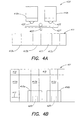
- the storage apparatus 321 comprises a load buffer as shown and described below with reference to FIGS. 4A and 4B.
- Each processing tool 319a-b has one or more tool loading platforms 323 coupled thereto, such that one or more wafer carriers may be transferred from the tool loading platform 323 to the respective processing tool 319, as is known in the art.
- the tool loading platform 323 comprises pod opening capability (i.e., the ability to open a sealed wafer carrier).
- the tool loading platform 323 is configured as described in U.S. Patent Application No. 09/012,323, filed on January 23, 1998 (AMAT No. 2569/ATD/MBE), which is incorporated herein by this reference.
- the storage apparatus 321 preferably comprises a vertical transfer mechanism (such as an elevator or a pick and place robot)and a horizontal transfer mechanism (such as a conveyor or a shelf coupled to a pick and place robot) as described in detail in U.S. Patent Application Serial No. 09/350,867.
- the storage apparatus 321 most preferably comprises a conveyor adapted to transfer a wafer carrier between processing tools 319, as described in U.S. Patent Application Serial No. 09/350,867, and as shown and described with reference to FIGS. 4A and 4B.
- FIGS. 4A and 4B are a top plan and a side elevational view, respectively, of a processing tool set 409 (comprising a pair of processing tools 410a-b) having a preferred storage apparatus 411 coupled thereto.
- the storage apparatus 411 comprises three vertical transfer mechanisms (e.g., elevators) 413a-c, each of which couples to a single horizontal transfer mechanism 415 (e.g., a conveyor).
- the number of vertical transfer mechanisms required varies from one FAB configuration to the next, depending on the number of tools in the set.
- the first vertical transfer mechanism 413a is positioned closest to the branch transport aisle 315 (FIG.
- each load port 417, 419 comprises a surface having a plurality of rolling elements. The surface may be lifted and lowered between the E15 load port 417 and the horizontal transfer mechanism.
- the horizontal transfer mechanism also comprises a plurality of rolling elements. Once a load port is in line with the horizontal transfer mechanism the rolling elements of the load port may be energized causing a wafer carrier positioned thereon to roll from the vertical transfer mechanism 413a onto the horizontal transfer mechanism 415.
- the horizontal transfer mechanism 415 comprises a plurality of dual compartment segments of rolling elements that are indexable between a transfer position and a storage position as described in U.S. Patent Application Serial No. 09/350,867.
- a wafer carrier may therefore be placed in storage or transferred across the horizontal transfer mechanism 415 to another one of the vertical transfer mechanisms 413b-c, which preferably comprises a surface of rolling elements that is in an elevated position adjacent the horizontal transfer mechanism 415. Thereafter the vertical transfer mechanism 413b-c lowers the surface of rolling elements, and the wafer carrier positioned thereon, to a position adjacent the respective processing tool 410a-b.
- a tool loader robot 423 is adapted to transfer wafer carriers between the storage apparatus 411 and a tool loading platform 425 of one or more of the processing tools 410a-b.
- a single tool loader robot 423 may be coupled to a rail 427 which extends in front of a plurality of processing tools 410a-b or each processing tool 410a-b may have a tool loader robot 423 dedicated thereto.
- the tool loader robot 423 may be omitted and the storage apparatus 411 may deliver a wafer carrier directly onto the tool loading platform 425.
- the wafer carrier may be transferred therefrom to the respective processing tool 410a-b for processing as is known in the art.
- the wafer carrier is a sealed pod (e.g., a Standard Mechanical Interface (SMIF) pod), or a Front Opening Unified Pod (FOUP)
- the tool loading platform 425 comprises a mechanism for opening the same without exposing the wafers to the surrounding atmosphere, also as is known in the art.
- SMIF Standard Mechanical Interface
- FOUP Front Opening Unified Pod
- the wafer carrier is then transferred to the vertical transfer mechanism 413a, elevated and either placed in storage or transferred along the horizontal transfer mechanism 415 to the second processing tool 410b (e.g., if the first and second processing tools 410a-b are adapted to perform sequential processes such as masking followed by etching) or to the E15 or overhead load ports 417, 419, respectively, where the wafer carrier is transferred to the branch transport aisle 315 (FIG. 3) for subsequent transfer to a second set of processing tools or for return to the central transport aisle 313 (FIG. 3) (e.g., for transfer to a second branch transport aisle).
- the common storage-movement apparatus receives a wafer carrier from the FAB and can move the wafer carrier to a position in which the wafer carrier may be accessed by a processing tool (i.e., directly onto a tool loading platform, or onto a tool load port from which the tool's loader robot may pick up the wafer carrier for transfer either directly to the tool or to the tool loading platform).
- a processing tool i.e., directly onto a tool loading platform, or onto a tool load port from which the tool's loader robot may pick up the wafer carrier for transfer either directly to the tool or to the tool loading platform.
- Each processing tool in a set may thus receive wafer carriers from the storage-movement apparatus, yet the FAB's control program contains information regarding only the factory load port(s) of the storage-movement apparatus and the information regarding capacity and processing necessary to schedule production.
- Processing tools may be added to or subtracted from a tool set without requiring new factory load port information to be added to the FAB's control program. Only the tool set parameters which reflect the set's internal capabilities, processes to be performed, capacity, etc., need be added to the FAB's control program. Because each processing tool is generally parallel to the branch transport aisle, processing tools can be added without requiring additional branch transport aisle length, elongation of aisles or addition of new aisles. Significant cost savings may be realized both in reduced branch transport aisle lengths and in reduced downtime during addition of fabrication tools. Thus, production capacity may be increased with less downtime.
- coupling a storage apparatus perpendicular to a branch transport aisle may enable processing tools to be added to a branch transport aisle without requiring elongation of the branch transport aisle and without requiring additional load ports (e.g., the E15 load port 417 or the overhead load port 419). Accordingly, a FAB can be incrementally expanded with minimal downtime.
- the horizontal transfer component of the storage apparatus is elongated so as to extend to a position adjacent the additional processing tool, and data is input to the MEMC program to reflect which set has been expanded, so that the flow of wafer carriers to and from the respective set can be increased accordingly.
- a method of reducing capital equipment costs without reducing fault tolerance is provided.
- one or more additional processing tools e.g., vacuum processing tools such as the Endura® or Centura® manufactured by Applied Materials, Inc. of Santa Clara, California
- periodic (e.g., monthly, weekly, yearly) payment are provided in exchange for periodic (e.g., monthly, weekly, yearly) payment.
- periodic payment may be conditioned on future use.
- a manufacturer has additional tool capacity which provides fault tolerance, yet does not have the initial capital investment cost of directly purchasing the additional processing tool(s). Further, this method allows the additional tool to be expensed rather than depreciated.
- the present invention can be used in any grid type layout (e.g., bay and chase, ballroom, etc.), and depending on the space limitations may be used in a pinwheel or cartwheel layout as are known in the art.
- the invention can be used with or without the optional clean room wall 27 (shown in phantom in FIG. 3).
- the processing tools may be vacuum tools (e.g., adapted for physical vapor deposition, chemical vapor deposition, etch, etc.) or environmentally controlled non-vacuum tools, e.g., adapted for chemical mechanical polishing, cleaning, metrology, etc.) and may employ a single processing chamber or a plurality of processing chambers.
- the central transport aisle 313 and the branch transport aisles 315 may contain any configuration of wafer transport and/or storage equipment, e.g., a storage apparatus such as that shown in FIG. 3, or such as described in U.S. Patent Application Serial No. 09/350,867 may be positioned parallel to the branch transport aisle and adapted to supply wafer carriers to the storage apparatuses 321 positioned perpendicular to the branch transport aisle 315.
- an incoming wafer carrier or lot may be divided into sublots and distributed to two or more processing tools in order to increase throughput.
Landscapes
- Container, Conveyance, Adherence, Positioning, Of Wafer (AREA)
- Stored Programmes (AREA)
- Safety Devices In Control Systems (AREA)
- Photosensitive Polymer And Photoresist Processing (AREA)
Abstract
Description
Claims (13)
- A fabrication system comprising:a branch transport aisle (315); andat least one fabrication tool set (317a-h, 409), each comprising:a storage-movement apparatus (321, 411) adapted to store wafer carriers, the apparatus (321, 411) being coupled to the branch transport aisle (315), and having one or more load ports (LP, 417) adapted to receive a wafer carrier from the branch transport aisle (315) or a factory transport agent;a first fabrication tool (319a, b; 410a, b) coupled to the storage apparatus (321, 411); anda first tool loading platform (425) adapted to receive a wafer carrier from the storage-movement apparatus (321, 411), the first tool loading platform (425) being positioned to enable the first fabrication tool to access a wafer carrier positioned thereon.
- The system of claim 1, wherein the storage-movement apparatus (321, 411) is coupled perpendicular to the branch transport aisle (315).
- The system of claim 1 or 2 further comprising:at least a second fabrication tool (319a, b; 410a, b) coupled to the branch transport aisle (315) and to the storage apparatus (321, 411); andat least a second tool loading platform (425) adapted to receive a wafer carrier from the storage apparatus (321, 411), the second tool loading platform (425) being positioned to enable the second fabrication tool (319a, b; 410a, b) to access a wafer carrier positioned thereon.
- The system of claim 1, 2 or 3, wherein at least one of the fabrication tools (319a, b; 410a, b) is coupled parallel to the branch transport aisle (315) and/or coupled perpendicular to the storage apparatus (321, 411).
- The system of any of the preceding claims, wherein the storage apparatus (321, 411) comprises a vertical component (413a, b, c) adapted to move wafer carriers vertically and a horizontal component (415) adapted to move wafer carriers horizontally.
- The system of any of the preceding claims, wherein the storage apparatus (321, 411) further comprises an overhead load port (419).
- The system of any of the preceding claims, wherein the load port (LP, 417) is an overhead load port (419).
- The system of any of the claims 3 to 7, wherein the first and second fabrication tools (319a, b; 410a, b) or at least one group of the fabrication tools (319a, b; 410a, b) are configured to perform identical processes.
- The system of any of the claims 3 to 7, wherein the first and second fabrication tools (319a, b; 410a, b) or at least one group of the fabrication tools (319a, b; 410a, b) are configured to perform different processes.
- A method of building a fabrication system, comprising:providing a branch transport aisle (315);coupling at least one storage apparatus (321, 411) to the branch transport aisle (315);coupling a first fabrication tool (319a, b; 410a, b) to the storage apparatus (321, 411) such that a wafer carrier may be received from the branch transport aisle (315) by the storage apparatus (321, 411) and transferred along the storage apparatus (321, 411) to a position adjacent the first fabrication tool (319a, b; 410a, b); andcoupling a second fabrication tool (319a, b; 410a, b) to the storage apparatus (321, 411) such that a wafer carrier may be received from the branch transport aisle (315) by the storage apparatus (321, 411) and transferred along the storage apparatus (321, 411) to a position adjacent the second fabrication tool (319a, b; 410a, b), the first fabrication tool (319a, b; 410a, b) being positioned beside the second fabrication tool, and between the second fabrication tool and the branch transport aisle (315).
- The method of claim 10 wherein coupling the at least one storage apparatus (321, 411) comprises coupling the at least one storage apparatus perpendicular to the branch transport aisle (315).
- The method of claim 10 or 11, wherein coupling a first fabrication tool (319a, b; 410a, b) comprises coupling the first fabrication tool (319a, b; 410a, b) perpendicular to the storage apparatus (321, 411) and parallel to the branch transport aisle (315); and coupling a second fabrication tool (319a, b; 410a, b) comprises coupling the second fabrication tool (319a, b; 410a, b) perpendicular to the storage apparatus (321, 411) and parallel to the branch transport aisle (315).
- The method of claim 10, 11 or 12, further comprising:providing a first pod opener and a second pod opener, each adapted to open a sealed wafer carrier and to allow one or more wafers to be extracted therefrom directly into a fabrication tool (319a, b; 410a, b) coupled thereto, without exposing the wafer to the environment surrounding the wafer carrier;positioning the first pod opener to receive a wafer carrier from the storage apparatus (321, 411) and to provide a wafer to the first fabrication tool (319a, b; 410a, b); andpositioning the second pod opener to receive a wafer carrier from the storage apparatus (321, 411) and to provide a wafer to the second fabrication tool (319a, b; 410a, b).
Applications Claiming Priority (2)
| Application Number | Priority Date | Filing Date | Title |
|---|---|---|---|
| US09/517,227 US6698991B1 (en) | 2000-03-02 | 2000-03-02 | Fabrication system with extensible equipment sets |
| US517227 | 2000-03-02 |
Publications (2)
| Publication Number | Publication Date |
|---|---|
| EP1132947A2 true EP1132947A2 (en) | 2001-09-12 |
| EP1132947A3 EP1132947A3 (en) | 2006-06-21 |
Family
ID=24058911
Family Applications (2)
| Application Number | Title | Priority Date | Filing Date |
|---|---|---|---|
| EP01104510A Withdrawn EP1146451A3 (en) | 2000-03-02 | 2001-03-02 | Fabrication system with extensible equipment sets |
| EP01104509A Withdrawn EP1132947A3 (en) | 2000-03-02 | 2001-03-02 | Fabrication system with extensible equipment sets |
Family Applications Before (1)
| Application Number | Title | Priority Date | Filing Date |
|---|---|---|---|
| EP01104510A Withdrawn EP1146451A3 (en) | 2000-03-02 | 2001-03-02 | Fabrication system with extensible equipment sets |
Country Status (5)
| Country | Link |
|---|---|
| US (1) | US6698991B1 (en) |
| EP (2) | EP1146451A3 (en) |
| JP (1) | JP2001308159A (en) |
| KR (1) | KR20010087300A (en) |
| TW (1) | TW498401B (en) |
Cited By (1)
| Publication number | Priority date | Publication date | Assignee | Title |
|---|---|---|---|---|
| DE10350517A1 (en) * | 2003-10-29 | 2005-06-09 | Sieghard Schiller Gmbh & Co. Kg | Holder for semiconductor wafer stack has robotic handling arm and separate stacks rotatable about a vertical axis for free access and transportation |
Families Citing this family (18)
| Publication number | Priority date | Publication date | Assignee | Title |
|---|---|---|---|---|
| JPH0936198A (en) * | 1995-07-19 | 1997-02-07 | Hitachi Ltd | Vacuum processing apparatus and semiconductor manufacturing line using the same |
| KR100454393B1 (en) * | 2001-12-18 | 2004-10-26 | 코스텍시스템(주) | Multi Vertical-type Single wafer-System apparatus for processing semiconductor wafer |
| WO2004001817A1 (en) * | 2002-06-21 | 2003-12-31 | Applied Materials, Inc. | Transfer chamber for vacuum processing system |
| KR100475120B1 (en) * | 2002-11-27 | 2005-03-10 | 삼성전자주식회사 | Fabrication system having double layered clean room for producing semiconductor device |
| US7031786B2 (en) * | 2004-03-25 | 2006-04-18 | Taiwan Semiconductor Manufacturing Co., Ltd. | System and method for fabrication backup planning |
| US7784164B2 (en) * | 2004-06-02 | 2010-08-31 | Applied Materials, Inc. | Electronic device manufacturing chamber method |
| CN103199039B (en) * | 2004-06-02 | 2016-01-13 | 应用材料公司 | Electron device manufacturing chamber and forming method thereof |
| US20130226329A1 (en) * | 2006-08-12 | 2013-08-29 | Frederick A. Flitsch | Cleanspace Fabricators for High Technology Manufacturing and Assembly Processing |
| US11024527B2 (en) | 2005-06-18 | 2021-06-01 | Frederick A. Flitsch | Methods and apparatus for novel fabricators with Cleanspace |
| US20080025821A1 (en) * | 2006-07-25 | 2008-01-31 | Applied Materials, Inc. | Octagon transfer chamber |
| US20080292433A1 (en) * | 2007-05-11 | 2008-11-27 | Bachrach Robert Z | Batch equipment robots and methods of array to array work-piece transfer for photovoltaic factory |
| US20080279658A1 (en) * | 2007-05-11 | 2008-11-13 | Bachrach Robert Z | Batch equipment robots and methods within equipment work-piece transfer for photovoltaic factory |
| US20080279672A1 (en) * | 2007-05-11 | 2008-11-13 | Bachrach Robert Z | Batch equipment robots and methods of stack to array work-piece transfer for photovoltaic factory |
| US7496423B2 (en) * | 2007-05-11 | 2009-02-24 | Applied Materials, Inc. | Method of achieving high productivity fault tolerant photovoltaic factory with batch array transfer robots |
| US9991139B2 (en) * | 2012-12-03 | 2018-06-05 | Asm Ip Holding B.V. | Modular vertical furnace processing system |
| WO2014104895A1 (en) * | 2012-12-31 | 2014-07-03 | Asm Ip Holding B.V. | Semiconductor processing assembly and facility |
| CN105680287B (en) * | 2016-03-21 | 2018-05-29 | 东莞市精和电子科技有限公司 | Electrical connector and production method thereof |
| JP2024131483A (en) * | 2023-03-16 | 2024-09-30 | キオクシア株式会社 | Semiconductor Manufacturing Equipment |
Family Cites Families (10)
| Publication number | Priority date | Publication date | Assignee | Title |
|---|---|---|---|---|
| JP2644912B2 (en) * | 1990-08-29 | 1997-08-25 | 株式会社日立製作所 | Vacuum processing apparatus and operating method thereof |
| DE69403890T2 (en) * | 1994-01-14 | 1998-01-08 | International Business Machines Corp., Armonk, N.Y. | Assembly / disassembly device for sealable pressurized transport containers |
| JPH0936198A (en) * | 1995-07-19 | 1997-02-07 | Hitachi Ltd | Vacuum processing apparatus and semiconductor manufacturing line using the same |
| US5980183A (en) * | 1997-04-14 | 1999-11-09 | Asyst Technologies, Inc. | Integrated intrabay buffer, delivery, and stocker system |
| JPH1159829A (en) * | 1997-08-08 | 1999-03-02 | Mitsubishi Electric Corp | Semiconductor wafer cassette transfer device, stocker used in semiconductor wafer cassette transfer device, stocker entry work control method, stocker exit work control method, automatic transfer vehicle control method, and stocker stock collation method used in semiconductor wafer cassette transfer device |
| US6235634B1 (en) * | 1997-10-08 | 2001-05-22 | Applied Komatsu Technology, Inc. | Modular substrate processing system |
| JPH11121582A (en) * | 1997-10-15 | 1999-04-30 | Mitsubishi Electric Corp | Semiconductor wafer manufacturing equipment control method and semiconductor wafer manufacturing equipment |
| US6082951A (en) * | 1998-01-23 | 2000-07-04 | Applied Materials, Inc. | Wafer cassette load station |
| US6087811A (en) * | 1998-12-09 | 2000-07-11 | Analog Modules, Inc. | Pulsed-output power supply with high power factor |
| US6435330B1 (en) * | 1998-12-18 | 2002-08-20 | Asyai Technologies, Inc. | In/out load port transfer mechanism |
-
2000
- 2000-03-02 US US09/517,227 patent/US6698991B1/en not_active Expired - Fee Related
-
2001
- 2001-01-12 TW TW090100800A patent/TW498401B/en not_active IP Right Cessation
- 2001-03-01 JP JP2001057083A patent/JP2001308159A/en not_active Withdrawn
- 2001-03-02 EP EP01104510A patent/EP1146451A3/en not_active Withdrawn
- 2001-03-02 KR KR1020010010908A patent/KR20010087300A/en not_active Withdrawn
- 2001-03-02 EP EP01104509A patent/EP1132947A3/en not_active Withdrawn
Cited By (1)
| Publication number | Priority date | Publication date | Assignee | Title |
|---|---|---|---|---|
| DE10350517A1 (en) * | 2003-10-29 | 2005-06-09 | Sieghard Schiller Gmbh & Co. Kg | Holder for semiconductor wafer stack has robotic handling arm and separate stacks rotatable about a vertical axis for free access and transportation |
Also Published As
| Publication number | Publication date |
|---|---|
| US6698991B1 (en) | 2004-03-02 |
| EP1132947A3 (en) | 2006-06-21 |
| EP1146451A3 (en) | 2001-11-14 |
| EP1146451A2 (en) | 2001-10-17 |
| JP2001308159A (en) | 2001-11-02 |
| KR20010087300A (en) | 2001-09-15 |
| TW498401B (en) | 2002-08-11 |
Similar Documents
| Publication | Publication Date | Title |
|---|---|---|
| US6698991B1 (en) | Fabrication system with extensible equipment sets | |
| US6979168B2 (en) | Method and apparatus for transferring substrate | |
| US6519504B1 (en) | Vacuum processing apparatus and semiconductor manufacturing line using the same | |
| US5445484A (en) | Vacuum processing system | |
| US8292563B2 (en) | Nonproductive wafer buffer module for substrate processing apparatus | |
| US6328768B1 (en) | Semiconductor device manufacturing line | |
| KR100666346B1 (en) | Substrate cleaning device and method | |
| JP3454034B2 (en) | Vacuum processing equipment | |
| US6672819B1 (en) | Vacuum processing apparatus and semiconductor manufacturing line using the same | |
| US20020141850A1 (en) | Semiconductor fabrication apparatus, pod carry apparatus, pod carry method, and semiconductor device production method | |
| JPH05136245A (en) | Semiconductor manufacturing equipment | |
| US20020153578A1 (en) | Wafer buffering system | |
| US20230215749A1 (en) | Logistics system in fabrication facility | |
| KR100317000B1 (en) | Stocker-Based Transfer System | |
| KR20250100163A (en) | Substrate transfer system |
Legal Events
| Date | Code | Title | Description |
|---|---|---|---|
| PUAI | Public reference made under article 153(3) epc to a published international application that has entered the european phase |
Free format text: ORIGINAL CODE: 0009012 |
|
| AK | Designated contracting states |
Kind code of ref document: A2 Designated state(s): AT BE CH CY DE DK ES FI FR GB GR IE IT LI LU MC NL PT SE TR |
|
| AX | Request for extension of the european patent |
Free format text: AL;LT;LV;MK;RO;SI |
|
| PUAL | Search report despatched |
Free format text: ORIGINAL CODE: 0009013 |
|
| AK | Designated contracting states |
Kind code of ref document: A3 Designated state(s): AT BE CH CY DE DK ES FI FR GB GR IE IT LI LU MC NL PT SE TR |
|
| AX | Request for extension of the european patent |
Extension state: AL LT LV MK RO SI |
|
| AKX | Designation fees paid | ||
| STAA | Information on the status of an ep patent application or granted ep patent |
Free format text: STATUS: THE APPLICATION IS DEEMED TO BE WITHDRAWN |
|
| 18D | Application deemed to be withdrawn |
Effective date: 20061022 |
|
| REG | Reference to a national code |
Ref country code: DE Ref legal event code: 8566 |