EP1132772A1 - Halftone phase shift photomask and blanks for halftone phase shift photomask for it and pattern forming method using this - Google Patents
Halftone phase shift photomask and blanks for halftone phase shift photomask for it and pattern forming method using this Download PDFInfo
- Publication number
- EP1132772A1 EP1132772A1 EP00953435A EP00953435A EP1132772A1 EP 1132772 A1 EP1132772 A1 EP 1132772A1 EP 00953435 A EP00953435 A EP 00953435A EP 00953435 A EP00953435 A EP 00953435A EP 1132772 A1 EP1132772 A1 EP 1132772A1
- Authority
- EP
- European Patent Office
- Prior art keywords
- phase shift
- halftone phase
- film
- shift mask
- irradiation
- Prior art date
- Legal status (The legal status is an assumption and is not a legal conclusion. Google has not performed a legal analysis and makes no representation as to the accuracy of the status listed.)
- Granted
Links
Images







Classifications
-
- H—ELECTRICITY
- H10—SEMICONDUCTOR DEVICES; ELECTRIC SOLID-STATE DEVICES NOT OTHERWISE PROVIDED FOR
- H10P—GENERIC PROCESSES OR APPARATUS FOR THE MANUFACTURE OR TREATMENT OF DEVICES COVERED BY CLASS H10
- H10P76/00—Manufacture or treatment of masks on semiconductor bodies, e.g. by lithography or photolithography
-
- G—PHYSICS
- G03—PHOTOGRAPHY; CINEMATOGRAPHY; ANALOGOUS TECHNIQUES USING WAVES OTHER THAN OPTICAL WAVES; ELECTROGRAPHY; HOLOGRAPHY
- G03F—PHOTOMECHANICAL PRODUCTION OF TEXTURED OR PATTERNED SURFACES, e.g. FOR PRINTING, FOR PROCESSING OF SEMICONDUCTOR DEVICES; MATERIALS THEREFOR; ORIGINALS THEREFOR; APPARATUS SPECIALLY ADAPTED THEREFOR
- G03F1/00—Originals for photomechanical production of textured or patterned surfaces, e.g., masks, photo-masks, reticles; Mask blanks or pellicles therefor; Containers specially adapted therefor; Preparation thereof
- G03F1/26—Phase shift masks [PSM]; PSM blanks; Preparation thereof
- G03F1/32—Attenuating PSM [att-PSM], e.g. halftone PSM or PSM having semi-transparent phase shift portion; Preparation thereof
-
- G—PHYSICS
- G03—PHOTOGRAPHY; CINEMATOGRAPHY; ANALOGOUS TECHNIQUES USING WAVES OTHER THAN OPTICAL WAVES; ELECTROGRAPHY; HOLOGRAPHY
- G03F—PHOTOMECHANICAL PRODUCTION OF TEXTURED OR PATTERNED SURFACES, e.g. FOR PRINTING, FOR PROCESSING OF SEMICONDUCTOR DEVICES; MATERIALS THEREFOR; ORIGINALS THEREFOR; APPARATUS SPECIALLY ADAPTED THEREFOR
- G03F1/00—Originals for photomechanical production of textured or patterned surfaces, e.g., masks, photo-masks, reticles; Mask blanks or pellicles therefor; Containers specially adapted therefor; Preparation thereof
- G03F1/26—Phase shift masks [PSM]; PSM blanks; Preparation thereof
- G03F1/34—Phase-edge PSM, e.g. chromeless PSM; Preparation thereof
Definitions
- the present invention relates generally to a photomask used for the fabrication of high-density integrated circuits such as LSIs, a photomask blank for the fabrication of such a photomask and a pattern-formation process using the same, and more particularly to a halftone phase shift photomask that enables projected images of minute size to be obtained, a halftone phase shift photomask blank for the fabrication of this halftone phase shift photomask and a pattern-formation process using the same.
- phase shift masks such as LSIS are fabricated by the repetition of a so-called lithography process using a photomask.
- phase shift masks such as set forth in JP-A 58-173744, JP-B 62-59296, etc. to the formation of microcircuits in particular have already been under investigation.
- the so-called halftone phase shift photomask such as one set forth in United States Patent No. 4,890,309, etc. has attracted attention in view of expedited practical applications.
- JP-A's 05-2259 and 05-127361 some proposals have been made in respect of arrangements and materials improved in yields and reduced in costs for the purpose of practical applications.
- Figs. 14(a) through 14(d) are illustrative of the principles of halftone phase shift lithography
- Figs. 15(a) through 15(d) are illustrative of a conventional process.
- Figs. 14(a) and 15(a) are each a sectional view of a photomask
- Figs. 14(b) and 15(b) are each illustrative of the amplitude of light on the photomask
- Figs. 14(c) and 15(c) are each illustrative of the amplitude of light on a wafer
- Figs. 14(a) through 14(d) are illustrative of the principles of halftone phase shift lithography
- Figs. 15(a) through 15(d) are illustrative of a conventional process.
- Figs. 14(a) and 15(a) are each a sectional view of a photomask
- Reference numerals 911 and 921 are each a transparent substrate, 922 a 100% light-blocking film, 912 a halftone phase shift film, and 913 and 923 are each incident light.
- halftone phase shift film used herein is intended a film, in a single layer or multilayer form, having functions of substantially reversing the phase of transmitting exposure light with respect to the phase of exposure light passing through the air having the same optical length and attenuating the intensity of the light.
- the 100% light-blocking film 922 formed of Cr or the like is provided on the substrate 921 formed of quartz glass or the like, as shown in Fig.
- the optimum phase angle is 180°
- the optimum transmittance is in the range of 1 to 20% (100% for the opening) as determined depending on the pattern to be transferred, transfer conditions, etc.
- a halftone phase shift mask must be fabricated in such a way as to meet its optimum phase angle and transmittance. Any deviation from the optimum values leads to changes in the correct exposure, etc., ending up with dimensional accuracy drops, a limited tolerance to focus, etc.
- the refractive index, extinction coefficient, thickness accuracy and thickness stability of the single layer or multilayer forming the halftone phase shift mask are of vital importance.
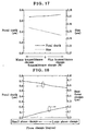
- Figs. 17 and 18 are illustrative of the results of simulation of what influences are produced by transmittance and phase difference changes on the depth of focus, transfer size and best focus change in lithography using a halftone phase shift mask.
- a problem with the halftone phase shift mask composed mainly of chromium and containing fluorine is, however, that its refractive index and/or its extinction coefficient change upon long-term irradiation with exposure light such as an ArF excimer laser.
- exposure light such as an ArF excimer laser.
- a resist pattern formed using a halftone phase shift photomask having the halftone phase shift film composed mainly of chromium and containing fluorine its transmittance and/or its phase angle change whenever it is used.
- an object of the present invention is to provide a halftone phase shift mask which does not vary in its refractive index and phase angle even upon irradiation with excimer laser used for exposure over an extended period of time, a blank for the fabrication of the same, and an image-formation process using the same.
- the present invention has been accomplished as a result of studies made so as to develop a halftone phase shift film which does not vary in its refractive index and phase angle even upon irradiation with excimer laser used for exposure over an extended period of time.
- a halftone phase shift mask blank comprising a halftone phase shift film containing at least chromium and fluorine on a transparent substrate, characterized in that: optical characteristic changes upon irradiation with an exposure excimer laser have been reduced by application of light of a wavelength substantially absorbed by said halftone phase shift film.
- a halftone phase shift mask blank comprising a halftone phase shift film containing at least chromium and fluorine on a transparent substrate, characterized in that: a protective film has been provided on said halftone phase shift mask to reduce optical characteristic changes upon irradiation with an exposure excimer laser.
- a halftone phase shift mask blank comprising a halftone phase shift film containing at least chromium and fluorine on a transparent substrate, characterized in that: optical characteristic changes upon irradiation with an exposure excimer laser have been reduced by application of light of a wavelength substantially absorbed by said halftone phase shift film, and provision of a protective layer on said halftone phase shift mask.
- a stabilized film has been formed on the surface of the halftone phase shift film by the application of light having a wavelength substantially absorbed by the halftone phase shift mask.
- the protective film contain at least chromium and fluorine with the content of fluorine being smaller than that in the halftone phase shift mask.
- the protective film be a transparent film.
- the transparent film may be composed mainly of a silicon oxide.
- a halftone phase shift mask comprising a halftone phase shift film pattern containing at least chromium and fluorine on a transparent substrate, characterized in that: optical characteristic changes upon irradiation with an exposure excimer laser have been reduced by patterning of a film irradiated with light having a wavelength substantially absorbed by said halftone phase shift film.
- a halftone phase shift mask comprising a halftone phase shift film pattern containing at least chromium and fluorine on a transparent substrate, characterized in that: optical characteristic changes upon irradiation with an exposure excimer laser have been reduced by application of light having a wavelength substantially absorbed by said halftone phase shift film after patterning of said halftone phase shift film.
- a halftone phase shift mask comprising a halftone phase shift film pattern containing at least chromium and fluorine on a transparent substrate, characterized in that: optical characteristic changes upon irradiation with an exposure excimer laser have been reduced by provision of a protective film pattern on said halftone phase shift film.
- a halftone phase shift mask having a halftone phase shift film pattern containing at least chromium and fluorine on a transparent substrate, characterized in that: optical characteristic changes upon irradiation with an exposure excimer laser have been reduced by provision of a protective film on the whole surface of said mask after patterning of said halftone phase shift film.
- the optical characteristic changes upon irradiation with an exposure excimer laser have been reduced by applying the light having a wavelength substantially absorbed by the halftone phase shift film, then providing a protective film thereon, and finally patterning the protective film and halftone phase shift film.
- the optical characteristic changes upon irradiation with an exposure excimer laser have been reduced by applying the light having a wavelength substantially absorbed by the halftone phase shift film, then patterning the film, and finally providing a protective film on the whole surface thereof.
- the optical characteristic changes upon irradiation with an exposure laser have been reduced by irradiating a patterned halftone phase shift film with the light having a wavelength substantially absorbed by said film, and then providing a protective film on the whole surface thereof.
- a stabilized film has been formed on the surface of the halftone phase shift film in contact with outside air by the application of the light having a wavelength substantially absorbed by said halftone phase shift film.
- the protective film contain at least chromium and fluorine with the content of fluorine being smaller than that in the halftone phase shift film.
- the protective film be a transparent film.
- the transparent film may be formed mainly of a silicon oxide.
- the pattern size be smaller than target size.
- the present invention comprises a pattern-formation process using any one of the aforesaid halftone phase shift masks.
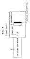
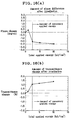
- Figs. 16(a) and 16(b) are illustrative of how the phase difference and transmittance of a halftone phase shift photomask containing at least chromium and fluorine change due to exposure to an excimer laser. That is, the changes in the phase difference and transmittance of a halftone phase shift film 5 with respect to the total applied energy are shown provided that using an irradiator as schematically shown in Fig.
- a halftone phase shift film 5 located in a sample chamber 3 was irradiated from the side of a glass substrate 4 with ArF excimer laser light (hereinafter called simply the laser) 2 from an ArF excimer laser system 1 under the conditions of pulse energy: 0.2 mJ/cm 2 /pulse, repetitive frequency: 1 kHz, and irradiation atmosphere: the air.
- the phase difference and transmittance were measured using MPM Phase Difference Meter, Laser Tech Co., Ltd.
- the composition of this halftone phase shift film was analyzed by X-ray photoelectron spectroscopy before and after the exposure light irradiation.
- the results are set out in Table 1 in the form of the ratio of atoms found in %.
- the halftone phase shift film was irradiated with the ArF excimer laser under the conditions of pulse energy: 0.2 mJ/cm 2 /pulse, total applied energy: 21.6 kJ/cm 2 , repetitive frequency: 1 kHz, and irradiation atmosphere: the air.
- the halftone phase shift photomask having a halftone phase shift film containing at least chromium and fluorine is irradiated, for instance, with the same excimer laser as the exposure light before used for exposure, so that the surface of the film is previously allowed to change in quality, thereby reducing the changes in the phase difference and transmittance of the film after the initiation of exposure.
- ArF excimer laser irradiation it is found from Fig. 16 that the previous application of the total applied energy of 2.5 kJ/cm 2 are sufficient to this end.
- an excimer laser similar to that actually used for exposure may be used for irradiation, it is understood that another light may be used with the proviso that it can be substantially absorbed by the halftone phase shift film.
- high pressure mercury-vapor lamps, xenon lamps, and deuterium lamps may be used for light sources.
- the irradiation of the halftone phase shift film with light may be carried out, with the same effect, from either the front or back side thereof.
- the irradiation should preferably be carried out in the air. However, this irradiation could be carried out, with the same effect, whether in a nitrogen atmosphere or in vacuum.
- the irradiation may be carried out simultaneously with the application of heat. In any case, it is only required to find the correlation between the total applied energy and the changes in transmittance and phase angle, as shown in Fig. 16, and apply the amount of energy greater than its point of inflection.
- this irradiation is not necessarily carried out after completion of the photomask fabrication process.
- the irradiation may be carried out at any time before the formation of a resist pattern using this photomask.
- the irradiation may be performed, with the same effect, whether in the process of making a photomask blank before forming the desired pattern or after the desired pattern has been formed. It follows that even when the irradiation is performed at any step after the halftone phase shift mask containing at least chromium and fluorine has been formed and before completion of the photomask, it is possible to reduce the changes in the transmittance and phase angle due to the aforesaid exposure.
- a halftone phase shift photomask having a stabilized phase difference and transmittance is actually fabricated according to the process of the present invention, it is preferable to form a halftone phase shift film on a transparent substrate while its phase angle and transmittance are determined in consideration of the aforesaid amount of change due to irradiation for stabilization.
- the present invention is also concerned with the provision of a protective film for preventing the aforesaid film quality change on the surface of a halftone phase shift film.
- this protective film for instance, is a film transparent to exposure light such as an SiO 2 film.
- the protective film does not only undergo such surface changes as shown in Table 1 even by irradiation with exposure light such as an ArF excimer laser but has also a function of preventing a halftone phase shift film containing at least chromium and fluorine from changing in quality, viz., decreasing in the content of fluorine with an increasing content of oxygen. It is thus possible to prevent the changes in the phase angle and transmittance of the halftone phase shift photomask due to exposure light irradiation.
- the protective film transparent films formed of metal fluorides and oxides such as MgF 2 , CaF 2 , LiF 2 , Al 2 O 3 , TiO 2 , ZrO 2 , HfO 2 , Ta 2 O 5 , ZnO, MgO and Mg 2 O 5 , to say nothing of the aforesaid SiO 2 , as well as and oxides of metal silicides such as CrSi, MoSi and WSi may be used.
- the desired effect of this protective film is achievable irrespective of where in the process of photomask fabrication it is formed.
- the protective film should be formed after the formation of the halftone phase shift film on the transparent substrate.
- the protective film a film translucent to exposure light, for instance, thin films formed of metals such as Mo and Cr.
- the translucent protective film should be formed before the photomask blank is processed into the desired pattern, and then processed into the same pattern simultaneously with the processing of the halftone phase shift film or at a separate step.
- the halftone phase shift film should be formed in such a way that when the protective film is provided, its transmittance and phase angle have the desired correlation between the opening portion and the pattern portion.
- the halftone phase shift film should preferably be formed with modification of pattern size in consideration of a possible change in transfer size due to transfer thereof to the section.
- the halftone phase shift film containing at least chromium and fluorine has substantially a multilayer structure, it is also effective to locate on the uppermost surface thereof a film that is most unlikely to undergo the aforesaid surface changes due to exposure light.
- a multilayer film containing at least chromium and fluorine in general, the more the content of fluorine, the more the content of oxygen is due to the aforesaid exposure, with a decreasing content of fluorine. In this case, it is desired to locate a film with a decreased content of fluorine on the surface of the multilayer structure.
- the application of the light having a substantially absorbed wavelength and the formation of the protective film - for the purpose of reducing the changes in transmittance and phase angle of the halftone phase shift film containing at least chromium and fluorine due to irradiation with exposure light such as an ArF excimer laser - have substantially the invariable effect irrespective of when carried out singularly or simultaneously.
- exposure light such as an ArF excimer laser -
- which of the application of the light having a substantially absorbed wavelength and the formation of the protective film is first carried out is of no precedence, and that they may be carried out somewhere in the process of photomask fabrication.
- the present invention relates to a halftone phase shift photomask wherein a halftone phase shift film containing at least chromium and fluorine is formed on a transparent substrate.
- the modification of these films or the provision of the protective film ensures that the halftone phase shift photomask is reduced in terms of the change in transmittance and phase angle during its storage or use, and eliminates or reduces various problems arising whenever the halftone phase shift mask is used such as a variation in the correct exposure, decreased dimensional accuracy, limited focus tolerance. limited pattern-formation tolerance, and degradation of pattern shape.
- Figs. 1(a) through 1(f) are illustrative of steps of fabricating a halftone phase shift mask blank according to Example 1 of the invention, and steps of processing the blank to obtain a halftone phase shift photomask.
- Figs. 2(a) through 2(d) are illustrative of steps of fabricating a halftone phase shift photomask according to Example 2 of the invention.
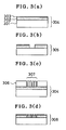
- Figs. 3(a) through 3d(f) are illustrative of steps of fabricating a halftone phase shift mask blank according to Example 3 of the invention, and steps of processing the blank to obtain a halftone phase shift photomask.
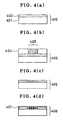
- Figs. 4(a) through 4(d) are illustrative of steps of fabricating a halftone phase shift photomask according to Example 4 of the invention.
- Figs. 5(a) through 5(e) are illustrative of steps of fabricating a halftone phase shift photomask according to Example 5 of the invention.
- Figs. 6(a) through 6(f) are illustrative of steps of fabricating a halftone phase shift photomask according to Example 6 of the invention.
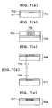
- Figs. 7(a) through 7(e) are illustrative of steps of fabricating a halftone phase shift photomask according to Example 7 of the invention.
- Fig. 8 is a schematic illustrative of an ArF excimer laser irradiator.
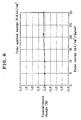
- Fig. 9 is a graphical representation illustrative of the results of experimentation on the resistance to ArF excimer laser irradiation of the halftone phase shift photomask according to Example 1 of the invention.
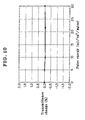
- Fig. 10 is a graphical representation illustrative of the results of experimentation on the resistance to ArF excimer laser irradiation of the halftone phase shift photomask according to Example 3 of the invention.
- Fig. 11 is illustrative of one construction of an aligner used at a resist pattern-formation step in Example 8 of the invention.
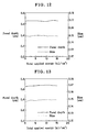
- Fig. 12 is a graphical representation illustrative of the results of experimentation wherein the resist pattern of Example 8 was formed using the halftone phase shift photomask according to Example 1 of the invention.
- Fig. 13 is a graphical representation illustrative of the results of experimentation wherein the resist pattern of Example 8 was formed using the halftone phase shift photomask according to Example 3 of the invention.
- Figs. 14(a) through 14(d) are illustrative of the principles of halftone phase shift lithography.
- Figs. 15(a) through 15(d) are illustrative of conventional lithography as compared with Figs. 14(a) through 14(d).
- Figs. 16(a) and 16(b) are graphical representations illustrative of how the phase difference and transmittance of a halftone phase shift photomask having a halftone phase shift film containing chromium and fluorine change due to excimer laser irradiation.
- Fig. 17 is a graphical representation illustrative of influences that transmittance changes have on the depth of focus and transfer size in lithography using a halftone phase shift photomask.
- Fig. 18 is a graphical representation illustrative of influences that phase difference changes have on the depth of focus and the best focus change in lithography using a halftone phase shift photomask.
- a halftone phase shift film 102 containing chromium and fluorine is formed on an optically polished, well-washed synthetic quartz substrate 101 by means of sputtering under the following conditions, thereby obtaining a halftone phase shift photomask blank 103.
- the formed halftone phase shift film 102 had a thickness of 135 nm.
- a sample 104 for measuring phase difference and transmittance was prepared by forming the halftone phase shift film 102 on the synthetic quartz substrate 101 at the same thickness under the same conditions, and patterning the halftone phase shift film by conventional lithography.
- the phase difference and transmittance at 193 nm wavelength of the halftone phase shift film was found to be about 182° and about 10%, respectively.
- the halftone phase shift photomask 103 was irradiated with laser light 109 of 193 nm wavelength, as shown in Fig. 1(c), thereby obtaining such a halftone phase shift mask blank 105 as shown in Fig. 1(d), which enabled the photomask to be used while its optical characteristic change was much reduced.
- the irradiation was carried out under the following conditions.
- the blank 103 was irradiated with the laser from the direction of the substrate 101.
- phase difference and transmittance-measuring sample 104 was irradiated under the aforesaid conditions to measure its phase difference and transmittance at 193 nm wavelength, which were found to be about 180° and about 11.5%, respectively.
- a commercially available electron beam resist (ZEP7000, Nippon Zeon Co., Ltd.) is coated on the halftone phase shift photomask blank 105 at a post-baking thickness of 300 nm, and subsequently baked at 110°C for 20 minutes to obtain an electron beam resist film 106. Then, using an electron beam lithography system for photomasks, a latent image in the desired pattern is obtained. Finally, this latent image is developed with a dedicated developing solution ZED500 to obtain the desired resist pattern 107.
- ZED500 dedicated developing solution
- the halftone phase shift film is surface treated with ozone while irradiated with ultraviolet radiation to remove an unnecessary portion of the resist, thereby obtaining such a halftone phase shift photomask 108 as shown in Fig. 1(f).
- the thus obtained halftone phase shift photomask 108 is much reduced in terms of phase difference and transmittance changes in the process of transfer and, hence, much improved in terms of practical utility, because it is fabricated using the blank with stabilized optical characteristics as shown in Fig. 9.
- a halftone phase shift film 202 containing chromium and fluorine is formed on an optically polished, well-washed synthetic quartz substrate 201 by means of sputtering under the following conditions, thereby obtaining a halftone phase shift photomask blank 203.
- the formed halftone phase shift film 202 had a thickness of 135 nm.
- a commercially available electron beam resist (ZEP7000, Nippon Zeon Co., Ltd.) is coated on this blank 203 at a post-baking thickness of 300 nm, and subsequently baked at 110°C for 20 minutes to obtain an electron beam resist film 204. Then, using an electron beam lithography system for photomasks, a latent image in the desired pattern is obtained. Finally, this latent image is developed with a dedicated developing solution ZED500 to obtain the desired resist pattern 205.
- ZED500 dedicated developing solution
- the halftone phase shift film is surface treated with ozone while irradiated with ultraviolet radiation to remove an unnecessary portion of the resist, thereby obtaining such a halftone phase shift photomask 206 as shown in Fig. 2(c).
- this halftone phase shift photomask 206 is well washed, and then irradiated with laser light 208 of 193 nm wavelength from the irradiator shown in Fig. 8, as in Example 1, thereby obtaining such a halftone phase shift photomask 207 as shown in Fig. 2(d), which can be used while its optical characteristic changes are much reduced.
- the irradiation is carried out under the same conditions as in Example 1.
- the thus obtained halftone phase shift photomask 207 is much reduced in terms of the changes in phase difference and transmittance in the process of transfer and, hence, much improved in terms of practical utility, because its optical characteristics have previously been varied as shown in Fig. 16 and reached a certain stable level.
- a halftone phase shift film 302 containing chromium and fluorine is formed on an optically polished, well-washed synthetic quartz substrate 301 by means of sputtering under the following conditions.
- the formed halftone phase shift film 302 had a thickness of 130 nm.
- an SiO 2 protective film 303 is formed on the halftone phase shift film 302 under the following conditions, thereby obtaining a halftone phase shift photomask blank 304.
- the formed protective film 303 had a thickness of 20 nm.
- a sample 305 for measuring phase difference and transmittance was prepared by forming the halftone phase shift film 302 and protective film 303 on the synthetic quartz substrate 301 at the same thickness under the same conditions, and patterning the protecting film 303 and halftone phase shift film 302 by conventional lithography.
- phase shift mask phase difference meter MPM193, Laser Tech Co., Ltd.
- the phase difference and transmittance at 193 nm wavelength of the halftone phase shift film was found to be about 180° and about 12%, respectively.
- a commercially available electron beam resist (ZEP7000, Nippon Zeon Co., Ltd.) is coated on the halftone phase shift photomask blank 304 at a post-baking thickness of 300 nm, and subsequently baked at 110°C for 20 minutes to obtain an electron beam resist film 306. Then, using an electron beam lithography system for photomasks, a latent image in the desired pattern is obtained. Finally, this latent image is developed with a dedicated developing solution ZED500 to obtain the desired resist pattern 307.
- ZED500 dedicated developing solution
- the halftone phase shift film is surface treated with ozone while irradiated with ultraviolet radiation to remove an unnecessary portion of the resist, thereby obtaining such a halftone phase shift photomask 308 as shown in Fig. 3(d).
- the thus obtained halftone phase shift photomask 308 is much reduced in terms of the changes in phase difference and transmittance in the process of transfer and, hence, much improved in terms of practical utility, because the optical characteristic changes shown in Fig. 16 are prevented by the formation of the protective film on the surface thereof.
- a further halftone phase shift photomask according to the present invention is explained with reference to Figs. 4(a) through 4(d).
- a halftone phase shift film 402 containing chromium and fluorine is formed on an optically polished, well-washed synthetic quartz substrate 401 by means of sputtering under the following conditions, thereby obtaining a halftone phase shift photomask blank 403.
- the formed halftone phase shift film 402 had a thickness of 135 nm.
- a commercially available electron beam resist (ZEP7000, Nippon Zeon Co., Ltd.) is coated on the this blank 403 at a post-baking thickness of 300 nm, and subsequently baked at 110°C for 20 minutes to obtain an electron beam resist film 404. Then, using an electron beam lithography system for photomasks, a latent image in the desired pattern is obtained. Finally, this latent image is developed with a dedicated developing solution ZED500 to obtain the desired resist pattern 405.
- ZED500 dedicated developing solution
- the halftone phase shift film is surface treated with ozone while irradiated with ultraviolet radiation to remove an unnecessary portion of the resist, thereby obtaining such a halftone phase shift photomask 406 as shown in Fig. 4(c).
- a protective film 407 is formed on this halftone phase shift photomask 406 under the following conditions, thereby obtaining a halftone phase shift photomask 408 with the protective film attached thereto.
- the formed protective film 407 had a thickness of 20 nm.
- the thus obtained halftone phase shift photomask 408 is much reduced in terms of the phase difference and transmittance changes in the process of transfer and, hence, much improved in terms of practical utility, because it is fabricated using the blank having stable optical characteristics with respect to ArF excimer laser irradiation, as shown in Fig. 10.
- a further halftone phase shift photomask according to the present invention is explained with reference to Figs. 5(a) through 5(e).
- a halftone phase shift film 502 containing chromium and fluorine is formed on an optically polished, well-washed synthetic quartz substrate 501 by means of sputtering under the following conditions, thereby obtaining a halftone phase shift photomask blank 503.
- the formed halftone phase shift film 502 had a thickness of 135 nm.
- a commercially available electron beam resist (ZEP7000, Nippon Zeon Co., Ltd.) is coated on this blank 503 at a post-baking thickness of 300 nm, and subsequently baked at 110°C for 20 minutes to obtain an electron beam resist film 504. Then, using an electron beam lithography system for photomasks, a latent image in the desired pattern is obtained. Finally, this latent image is developed with a dedicated developing solution ZED500 to obtain the desired resist pattern 505.
- the halftone phase shift film is surface treated with ozone while irradiated with ultraviolet radiation to remove an unnecessary portion of the resist, thereby obtaining such a halftone phase shift photomask 506 as shown in Fig. 5(c).
- this halftone phase shift photomask 506 is well washed, and then irradiated with laser light 208 of 193 nm wavelength from the irradiator shown in Fig. 8, as in Examples 1 and 2, thereby obtaining such a halftone phase shift photomask 507 as shown in Fig. 5(d), which can be used while its optical characteristic changes are much reduced.
- the irradiation is carried out under the same conditions as in Examples 1 and 2.
- an SiO 2 protective film 509 is formed on the whole surface of this halftone phase shift photomask 507 under the following conditions, thereby obtaining a halftone phase shift photomask 510 with the protective film attached thereto.
- the formed protective film 509 had a thickness of 20 nm.
- the thus obtained halftone phase shift photomask 510 is much reduced in terms of the changes in phase difference and transmittance in the process of transfer and, hence, much improved in terms of practical utility, because the optical characteristic changes shown in Fig. 16 are prevented by the formation of the protective film 509 on the surface thereof.
- a further halftone phase shift photomask according to the present invention is explained with reference to Figs. 6(a) through 6(f).
- a halftone phase shift film 602 containing chromium and fluorine is formed on an optically polished, well-washed synthetic quartz substrate 601 by means of sputtering under the following conditions, thereby obtaining a halftone phase shift photomask blank 603.
- the formed halftone phase shift film 602 had a thickness of 130 nm.
- an SiO 2 protective film 604 is formed on the halftone phase shift film under the following conditions as shown in Fig. 6(b), thereby obtaining a halftone phase shift photomask blank 605.
- the formed protective film 604 had a thickness of 20 nm.
- a commercially available electron beam resist (ZEP7000, Nippon Zeon Co., Ltd.) is coated on the halftone phase shift photomask blank 605 at a post-baking thickness of 300 nm, and subsequently baked at 110°C for 20 minutes to obtain an electron beam resist film 606. Then, using an electron beam lithography system for photomasks, a latent image in the desired pattern is obtained. Finally, this latent image is developed with a dedicated developing solution ZED500 to obtain the desired resist pattern 607.
- ZED500 dedicated developing solution
- the halftone phase shift film is surface treated with ozone while irradiated with ultraviolet radiation to remove an unnecessary portion of the resist, thereby obtaining such a halftone phase shift photomask 608 as shown in Fig. 6(d).
- the halftone phase shift photomask 608 is well-washed, and then irradiated with laser light 610 of 193 nm wavelength from the irradiator shown in Fig. 8, as in Example 1, thereby obtaining such a halftone phase shift mask 609 as shown in Fig. 6(f), which can be used while it is much reduced in terms of optical characteristic changes.
- the irradiation is carried out under the same conditions as in
- the thus obtained halftone phase shift photomask 609 is much reduced in terms of phase difference and transmittance in the process of transfer and, hence, much improved in terms of practical utility, because the optical characteristic changes shown in Fig. 6 have previously be varied until a certain stable level has been reached.
- a further halftone phase shift photomask blank according to the present invention is explained with reference to Figs. 7(a) through 7(e).
- a halftone phase shift film 702 containing chromium and fluorine is formed on an optically polished, well-washed synthetic quartz substrate 701 by means of sputtering under the following conditions, thereby obtaining a halftone phase shift photomask blank 703.
- the formed halftone phase shift film 702 had a thickness of 135 nm.
- a commercially available electron beam resist (ZEP7000, Nippon Zeon Co., Ltd.) is coated on this blank 703 at a post-baking thickness of 300 nm, and subsequently baked at 110°C for 20 minutes to obtain an electron beam resist film 704.
- ZED7000 commercially available electron beam resist
- a latent image in the desired pattern is formed, provided however that the size of openings in the pattern is larger than the original opening size.
- this latent image is developed with a dedicated developing solution ZED500 to obtain a resist pattern 705 having an opening portion larger than the desired opening size.
- the halftone phase shift film is surface treated with ozone while irradiated with ultraviolet radiation to remove an unnecessary portion of the resist, thereby obtaining such a halftone phase shift photomask 706 as shown in Fig. 7(c).
- This halftone phase shift photomask 706 has an opening portion 710 larger than the desired size of an opening portion 709 in a halftone phase shift photomask 711 as shown in Fig. 7(d).
- a protective film 704 is formed on the halftone phase shift photomask 706 under the following conditions as shown in Fig. 7(e), thereby obtaining a halftone phase shift photomask 708 with the protective film attached thereto.
- the protective film 707 should be formed at such a thickness that the aforesaid opening portion has the desired patterning opening size by deposition of the protective film onto the pattern section.
- the desired opening size could be obtained by patterning the halftone phase shift film 702 while the opening size was 20 nm larger than the desired value on each side, and forming the protective film 707 at a thickness of 50 nm.
- the thus obtained halftone phase shift photomask 708 is much reduced in terms of phase difference and transmittance changes in the process of transfer and, hence, much improved in terms of practical utility, because the optical characteristic changes shown in Fig. 16 are prevented by the formation of the protective film 707 on the surface thereof.
- a halftone phase shift photomask 10 according to the present invention was positioned in a semiconductor aligner of such construction as shown in Fig. 11. Then, a halftone mask pattern was projected onto a wafer 12 on which a resist was coated using an ArF excimer laser 11 of 193 nm wavelength.
- the wafer 12 was coated thereon with DUV-30, Nissan Chemical Industries, Ltd., then baked at a given temperature, then coated thereon with ZAF001, Nippon Zeon Co., Ltd., and finally baked at a given temperature. After this, the wafer was exposed to light using a 193 nm wavelength ArF excimer laser aligner of Fig. 11, followed by backing at a given temperature, and development.
- Fig. 12 is a graphical representation illustrative of the results of transfer using the halftone phase shift photomask of Example 1 of the invention
- Fig. 13 is a graphical representation illustrative of the results of transfer using the halftone phase shift photomask of Example 3.
- the quantity of light exposed to the mask of the present invention is 15 kJ/cm 2 amounting to a 1.5 year worth of usual semiconductor exposure. This implies that the robustness of the halftone mask can be ensured by irradiation with energy radiation.
- a halftone phase shift film - which may be modified by irradiation with exposure light while actually used - is modified before put to practical use and/or a protective film for preventing such modification is provided, so that changes in phase difference and transmittance while the mask is used can be much reduced. It is thus possible to achieve practically much improved halftone phase shift photomasks and blanks therefor.
Landscapes
- Physics & Mathematics (AREA)
- General Physics & Mathematics (AREA)
- Preparing Plates And Mask In Photomechanical Process (AREA)
- Exposure And Positioning Against Photoresist Photosensitive Materials (AREA)
- Exposure Of Semiconductors, Excluding Electron Or Ion Beam Exposure (AREA)
Abstract
Description
optical characteristic changes upon irradiation with an exposure excimer laser have been reduced by application of light of a wavelength substantially absorbed by said halftone phase shift film.
a protective film has been provided on said halftone phase shift mask to reduce optical characteristic changes upon irradiation with an exposure excimer laser.
optical characteristic changes upon irradiation with an exposure excimer laser have been reduced by application of light of a wavelength substantially absorbed by said halftone phase shift film, and provision of a protective layer on said halftone phase shift mask.
optical characteristic changes upon irradiation with an exposure excimer laser have been reduced by patterning of a film irradiated with light having a wavelength substantially absorbed by said halftone phase shift film.
optical characteristic changes upon irradiation with an exposure excimer laser have been reduced by application of light having a wavelength substantially absorbed by said halftone phase shift film after patterning of said halftone phase shift film.
optical characteristic changes upon irradiation with an exposure excimer laser have been reduced by provision of a protective film pattern on said halftone phase shift film.
optical characteristic changes upon irradiation with an exposure excimer laser have been reduced by provision of a protective film on the whole surface of said mask after patterning of said halftone phase shift film.
| Film Composition Before and After Exposure Light IRRADIATION (XPS Analysis) | ||||
| - | Cr | F | C | O |
| On Film Before Exposure | 14 | 27 | 31 | 28 |
| Surface After Exposure | 14 | 17 | 34 | 35 |
| In Film Before | 25 | 55 | 10 | 10 |
| After | 25 | 55 | 10 | 10 |
Etching system: Parallel-plate reactive ion etcher
Etching system: Parallel-plate reactive ion etcher
Claims (20)
- A halftone phase shift mask blank comprising a halftone phase shift film containing at least chromium and fluorine on a transparent substrate, wherein:
optical characteristic changes upon irradiation with an exposure excimer laser have been reduced by application of light of a wavelength substantially absorbed by said halftone phase shift film. - A halftone phase shift mask blank comprising a halftone phase shift film containing at least chromium and fluorine on a transparent substrate, wherein:
a protective film has been provided on said halftone phase shift mask to reduce optical characteristic changes upon irradiation with an exposure excimer laser. - A halftone phase shift mask blank comprising a halftone phase shift film containing at least chromium and fluorine on a transparent substrate, wherein:
optical characteristic changes upon irradiation with an exposure excimer laser have been reduced by application of light of a wavelength substantially absorbed by said halftone phase shift film, and provision of a protective layer on said halftone phase shift mask. - The halftone phase shift mask blank according to claim 1 or 3, wherein a stabilized film has been formed on the surface of the halftone phase shift film by the application of light having a wavelength substantially absorbed by the halftone phase shift mask.
- The halftone phase shift mask blank according to any one of claims 2 to 4, wherein the protective film contains at least chromium and fluorine with the content of fluorine being smaller than that in the halftone phase shift mask.
- The halftone phase shift mask blank according to any one of claims 2 to 4, wherein the protective film is a transparent film.
- The halftone phase shift mask blank according to any one of claims 2, 3, 4 and 6, wherein the protective film is mainly made up of a silicon oxide.
- A halftone phase shift mask comprising a halftone phase shift film pattern containing at least chromium and fluorine on a transparent substrate, wherein:
optical characteristic changes upon irradiation with an exposure excimer laser have been reduced by patterning of a film irradiated with light having a wavelength substantially absorbed by said halftone phase shift film. - A halftone phase shift mask comprising a halftone phase shift film pattern containing at least chromium and fluorine on a transparent substrate, wherein:
optical characteristic changes upon irradiation with an exposure excimer laser have been reduced by application of light having a wavelength substantially absorbed by said halftone phase shift film after patterning of said halftone phase shift film. - A halftone phase shift mask comprising a halftone phase shift film pattern containing at least chromium and fluorine on a transparent substrate, wherein:
optical characteristic changes upon irradiation with an exposure excimer laser have been reduced by provision of a protective film pattern on said halftone phase shift film. - A alftone phase shift mask having a halftone phase shift film pattern containing at least chromium and fluorine on a transparent substrate, wherein:
optical characteristic changes upon irradiation with an exposure excimer laser have been reduced by provision of a protective film on the whole surface of said mask after patterning of said halftone phase shift film. - The halftone phase shift mask according to claim 8, wherein the optical characteristic change upon irradiation with an exposure excimer laser have been reduced by applying the light having a wavelength substantially absorbed by the halftone phase shift film, then providing a protective film thereon, and finally patterning the protective film and halftone phase shift film.
- The halftone phase shift mask according to claim 8, wherein the optical characteristic changes upon irradiation with an exposure excimer laser have been reduced by applying the light having a wavelength substantially absorbed by the halftone phase shift film, then patterning the film, and finally providing a protective film on the whole surface thereof.
- The halftone phase shift mask according to claim 9, wherein the optical characteristic changes upon irradiation with an exposure laser have been reduced by irradiating a patterned halftone phase shift film with the light having a wavelength substantially absorbed by said film, and then providing a protective film on the whole surface thereof.
- The halftone phase shift mask according to any one of claims 8, 9, 12, 13 and 14, wherein a stabilized film has been formed on the surface of the halftone phase shift film in contact with outside air by the application of the light having a wavelength substantially absorbed by said halftone phase shift film.
- The halftone phase shift mask according to any one of claims 10 to 15, wherein the protective film contains at least chromium and fluorine with the content of fluorine being smaller than that in the halftone phase shift film.
- The halftone phase shift mask according to any one of claims 10 to 15, wherein the protective film is a transparent film.
- The halftone phase shift mask according to any one of claims 10 to 15 and 17, wherein the protective film is a film mainly made up of a silicon oxide.
- The halftone phase shift mask according to any one of claims 9, 10 and 13 to 18, wherein a pattern is formed with pattern size smaller than target size.
- A pattern-formation process using the halftone phase shift mask according to any one of claims 8 to 19.
Applications Claiming Priority (3)
| Application Number | Priority Date | Filing Date | Title |
|---|---|---|---|
| JP23118099 | 1999-08-18 | ||
| JP23118099A JP4197378B2 (en) | 1999-08-18 | 1999-08-18 | Halftone phase shift photomask, blank for halftone phase shift photomask for the same, and pattern formation method using the same |
| PCT/JP2000/005472 WO2001013178A1 (en) | 1999-08-18 | 2000-08-16 | Halftone phase shift photomask and blanks for halftone phase shift photomask for it and pattern forming method using this |
Publications (3)
| Publication Number | Publication Date |
|---|---|
| EP1132772A1 true EP1132772A1 (en) | 2001-09-12 |
| EP1132772A4 EP1132772A4 (en) | 2003-11-19 |
| EP1132772B1 EP1132772B1 (en) | 2007-10-17 |
Family
ID=16919585
Family Applications (1)
| Application Number | Title | Priority Date | Filing Date |
|---|---|---|---|
| EP00953435A Expired - Lifetime EP1132772B1 (en) | 1999-08-18 | 2000-08-16 | Halftone phase shift photomask and blank for it, and pattern forming method using this mask |
Country Status (7)
| Country | Link |
|---|---|
| US (1) | US6709791B1 (en) |
| EP (1) | EP1132772B1 (en) |
| JP (1) | JP4197378B2 (en) |
| KR (1) | KR100756115B1 (en) |
| DE (1) | DE60036779T2 (en) |
| TW (1) | TW502131B (en) |
| WO (1) | WO2001013178A1 (en) |
Cited By (3)
| Publication number | Priority date | Publication date | Assignee | Title |
|---|---|---|---|---|
| EP1426820A3 (en) * | 2002-12-03 | 2004-12-29 | Shin-Etsu Chemical Co., Ltd. | Methods of manufacturing photomask blank and photomask |
| EP1722271A3 (en) * | 2005-05-12 | 2007-07-18 | Shin-Etsu Chemical Co., Ltd. | Phase-shift photomask-blank, phase-shift photomask and fabrication method thereof |
| DE10223113B4 (en) * | 2002-05-21 | 2007-09-13 | Infineon Technologies Ag | Process for producing a photolithographic mask |
Families Citing this family (13)
| Publication number | Priority date | Publication date | Assignee | Title |
|---|---|---|---|---|
| KR100472721B1 (en) * | 2002-07-19 | 2005-03-10 | 주식회사 하이닉스반도체 | Reticle for photolithography |
| JP2007503621A (en) * | 2003-08-25 | 2007-02-22 | トッパン、フォウタマスクス、インク | Photomask and method for maintaining its optical properties |
| US20080261122A1 (en) * | 2007-04-20 | 2008-10-23 | Jeffrey Peter Gambino | Photolithography mask with protective capping layer |
| US20080261120A1 (en) * | 2007-04-20 | 2008-10-23 | Jeffrey Peter Gambino | Photolithography mask with integrally formed protective capping layer |
| US20080261121A1 (en) * | 2007-04-20 | 2008-10-23 | Jeffrey Peter Gambino | Photolithography mask with protective silicide capping layer |
| JP4714180B2 (en) | 2007-05-01 | 2011-06-29 | 株式会社東芝 | Photomask management method, photomask cleaning possible number generation method, and photomask management system |
| US8685596B2 (en) * | 2007-12-04 | 2014-04-01 | Sharp Laboratories Of America, Inc. | Semi-transparent film grayscale mask |
| US20100119958A1 (en) * | 2008-11-11 | 2010-05-13 | Taiwan Semiconductor Manufacturing Co., Ltd. | Mask blank, mask formed from the blank, and method of forming a mask |
| JP2011065113A (en) * | 2009-09-21 | 2011-03-31 | Toshiba Corp | Phase shift mask, method of manufacturing the same, and method of manufacturing semiconductor device |
| JP6295352B2 (en) * | 2017-03-01 | 2018-03-14 | Hoya株式会社 | Mask blank manufacturing method, phase shift mask manufacturing method, and semiconductor device manufacturing method |
| CN112180676A (en) * | 2020-09-23 | 2021-01-05 | 武汉华星光电技术有限公司 | Halftone mask, display panel preparation method and ultraviolet mask |
| JP2023111619A (en) * | 2022-01-31 | 2023-08-10 | 株式会社トッパンフォトマスク | PHASE SHIFT MASK AND METHOD FOR MANUFACTURING PHASE SHIFT MASK |
| US20250284200A1 (en) * | 2024-03-11 | 2025-09-11 | Applied Materials, Inc. | Diffuser-less gray-tone lithography process, mask design, and fabrication method |
Family Cites Families (20)
| Publication number | Priority date | Publication date | Assignee | Title |
|---|---|---|---|---|
| JPS6086545A (en) * | 1983-10-17 | 1985-05-16 | Fujitsu Ltd | Mask protective film |
| JPH0652421B2 (en) * | 1987-09-30 | 1994-07-06 | シャープ株式会社 | Photo mask |
| US5260150A (en) * | 1987-09-30 | 1993-11-09 | Sharp Kabushiki Kaisha | Photo-mask with light shielding film buried in substrate |
| JPH02186348A (en) * | 1989-01-12 | 1990-07-20 | Seiko Epson Corp | Method of forming surface protective film |
| JPH03131027A (en) * | 1989-10-17 | 1991-06-04 | Oki Electric Ind Co Ltd | High speed heat treating method and device therefor |
| JPH03278524A (en) * | 1990-03-28 | 1991-12-10 | Nec Corp | Heating apparatus of semiconductor device |
| JP3210705B2 (en) * | 1991-11-12 | 2001-09-17 | 大日本印刷株式会社 | Phase shift photomask |
| US5380608A (en) * | 1991-11-12 | 1995-01-10 | Dai Nippon Printing Co., Ltd. | Phase shift photomask comprising a layer of aluminum oxide with magnesium oxide |
| US5629115A (en) * | 1993-04-30 | 1997-05-13 | Kabushiki Kaisha Toshiba | Exposure mask and method and apparatus for manufacturing the same |
| JP3253783B2 (en) * | 1993-08-13 | 2002-02-04 | 株式会社東芝 | Halftone phase shift mask and method of manufacturing the same |
| JPH0745595A (en) * | 1993-07-29 | 1995-02-14 | Dainippon Printing Co Ltd | Patterning method for semiconductor device |
| JPH07295203A (en) * | 1994-04-27 | 1995-11-10 | Dainippon Printing Co Ltd | Method for manufacturing blanks for halftone phase shift photomask |
| JP3262303B2 (en) * | 1993-08-17 | 2002-03-04 | 大日本印刷株式会社 | Halftone phase shift photomask and blank for halftone phase shift photomask |
| KR100311704B1 (en) * | 1993-08-17 | 2001-12-15 | 기타오카 다카시 | Halftone Phase Shift Photomask, Blanks for Halftone Phase Shift Photomask and Manufacturing Method of the Blanks |
| JPH07248609A (en) * | 1994-03-11 | 1995-09-26 | Hoya Corp | Phase shift mask blank and phase shift mask |
| JPH0943830A (en) * | 1995-08-03 | 1997-02-14 | Hoya Corp | Halftone type phase shift mask, halftone type phase shift mask blank and manufacturing method thereof |
| JPH09244212A (en) * | 1996-03-12 | 1997-09-19 | Dainippon Printing Co Ltd | Halftone phase shift photomask and blank for halftone phase shift photomask |
| JP2988417B2 (en) * | 1997-02-28 | 1999-12-13 | 日本電気株式会社 | Photo mask |
| JPH1126355A (en) * | 1997-07-07 | 1999-01-29 | Toshiba Corp | Exposure mask and method of manufacturing the same |
| JP2000330264A (en) * | 1999-05-19 | 2000-11-30 | Nikon Corp | Method for manufacturing transfer mask blanks |
-
1999
- 1999-08-18 JP JP23118099A patent/JP4197378B2/en not_active Expired - Lifetime
-
2000
- 2000-08-16 DE DE60036779T patent/DE60036779T2/en not_active Expired - Fee Related
- 2000-08-16 KR KR1020017004808A patent/KR100756115B1/en not_active Expired - Fee Related
- 2000-08-16 EP EP00953435A patent/EP1132772B1/en not_active Expired - Lifetime
- 2000-08-16 WO PCT/JP2000/005472 patent/WO2001013178A1/en not_active Ceased
- 2000-08-16 US US09/807,276 patent/US6709791B1/en not_active Expired - Lifetime
- 2000-08-17 TW TW089116613A patent/TW502131B/en not_active IP Right Cessation
Cited By (6)
| Publication number | Priority date | Publication date | Assignee | Title |
|---|---|---|---|---|
| DE10223113B4 (en) * | 2002-05-21 | 2007-09-13 | Infineon Technologies Ag | Process for producing a photolithographic mask |
| EP1426820A3 (en) * | 2002-12-03 | 2004-12-29 | Shin-Etsu Chemical Co., Ltd. | Methods of manufacturing photomask blank and photomask |
| US7195846B2 (en) | 2002-12-03 | 2007-03-27 | Shin-Etsu Chemical Co., Ltd. | Methods of manufacturing photomask blank and photomask |
| KR100843417B1 (en) * | 2002-12-03 | 2008-07-03 | 신에쓰 가가꾸 고교 가부시끼가이샤 | Methods of Manufacturing Photomask Blank and Photomask |
| EP1722271A3 (en) * | 2005-05-12 | 2007-07-18 | Shin-Etsu Chemical Co., Ltd. | Phase-shift photomask-blank, phase-shift photomask and fabrication method thereof |
| US7622227B2 (en) | 2005-05-12 | 2009-11-24 | Shin-Etsu Chemical Co., Ltd | Phase-shift photomask-blank, phase-shift photomask and fabrication method thereof |
Also Published As
| Publication number | Publication date |
|---|---|
| KR20010085933A (en) | 2001-09-07 |
| WO2001013178A1 (en) | 2001-02-22 |
| US6709791B1 (en) | 2004-03-23 |
| KR100756115B1 (en) | 2007-09-05 |
| DE60036779T2 (en) | 2008-07-24 |
| JP4197378B2 (en) | 2008-12-17 |
| EP1132772A4 (en) | 2003-11-19 |
| JP2001056544A (en) | 2001-02-27 |
| EP1132772B1 (en) | 2007-10-17 |
| DE60036779D1 (en) | 2007-11-29 |
| TW502131B (en) | 2002-09-11 |
Similar Documents
| Publication | Publication Date | Title |
|---|---|---|
| US6913706B2 (en) | Double-metal EUV mask absorber | |
| US6709791B1 (en) | Halftone phase shift photomask and blanks for halftone phase shift photomask for it and pattern forming method using this | |
| US5721075A (en) | Blanks for halftone phase shift photomasks, halftone phase shift photomasks, and methods for fabricating them | |
| US20020061452A1 (en) | Phase shift mask blank, phase shift mask, and method for manufacturing the same | |
| KR100843417B1 (en) | Methods of Manufacturing Photomask Blank and Photomask | |
| US7026077B2 (en) | Photomask blank manufacturing method | |
| EP1116999B1 (en) | Phase shift mask blank, phase shift mask and method of manufacture | |
| US6764792B1 (en) | Halftone phase shift photomask and blanks for halftone phase shift photomask for producing it | |
| EP1381918A2 (en) | Ion-beam deposition process for manufacturing multilayered attenuated phase shift photomask blanks | |
| US6503668B2 (en) | Phase shift mask blank, phase shift mask, and method of manufacture | |
| EP0582308A2 (en) | Photomask blank and phase shift photomask | |
| JP3351892B2 (en) | Halftone phase shift photomask and blank for halftone phase shift photomask | |
| JPH04162039A (en) | Photomask | |
| JP3301556B2 (en) | Phase shift photomask blank and phase shift photomask | |
| EP1143295B1 (en) | Halftone phase shifting photomask and blanks therefor and a method for forming a pattern using said mask | |
| US6514642B2 (en) | Phase shift mask and method of manufacture | |
| JPH07295203A (en) | Method for manufacturing blanks for halftone phase shift photomask | |
| JPH1184624A (en) | Blank for halftone type phase shift mask, halftone type phase shift mask, and manufacturing method thereof | |
| JP3332230B2 (en) | Halftone phase shift photomask and blank for halftone phase shift photomask | |
| JPH09244211A (en) | Blank for halftone phase shift photomask, halftone phase shift photomask and manufacturing method thereof | |
| KR20010082981A (en) | Phase shift mask using CrAlO(N)F as a phase shift material and manufacturing method thereof |
Legal Events
| Date | Code | Title | Description |
|---|---|---|---|
| PUAI | Public reference made under article 153(3) epc to a published international application that has entered the european phase |
Free format text: ORIGINAL CODE: 0009012 |
|
| 17P | Request for examination filed |
Effective date: 20010511 |
|
| AK | Designated contracting states |
Kind code of ref document: A1 Designated state(s): AT BE CH CY DE DK ES FI FR GB GR IE IT LI LU MC NL PT SE |
|
| A4 | Supplementary search report drawn up and despatched |
Effective date: 20031007 |
|
| RIC1 | Information provided on ipc code assigned before grant |
Ipc: 7H 01L 21/027 B Ipc: 7G 03F 1/00 B Ipc: 7G 03F 1/14 B Ipc: 7G 03F 1/08 A |
|
| 17Q | First examination report despatched |
Effective date: 20040211 |
|
| RBV | Designated contracting states (corrected) |
Designated state(s): DE FR IT |
|
| 17Q | First examination report despatched |
Effective date: 20040211 |
|
| RAP1 | Party data changed (applicant data changed or rights of an application transferred) |
Owner name: DAI NIPPON PRINTING CO., LTD. |
|
| RTI1 | Title (correction) |
Free format text: HALFTONE PHASE SHIFT PHOTOMASK AND BLANK FOR IT, AND PATTERN FORMING METHOD USING THIS MASK |
|
| GRAJ | Information related to disapproval of communication of intention to grant by the applicant or resumption of examination proceedings by the epo deleted |
Free format text: ORIGINAL CODE: EPIDOSDIGR1 |
|
| GRAP | Despatch of communication of intention to grant a patent |
Free format text: ORIGINAL CODE: EPIDOSNIGR1 |
|
| GRAP | Despatch of communication of intention to grant a patent |
Free format text: ORIGINAL CODE: EPIDOSNIGR1 |
|
| GRAS | Grant fee paid |
Free format text: ORIGINAL CODE: EPIDOSNIGR3 |
|
| RIN1 | Information on inventor provided before grant (corrected) |
Inventor name: ONODERA,TOSHIOSEMICONDUCTOR LEADING EDGE TECH INC Inventor name: MOHRI, HIROSHI,C/O DAI NIPPON PRINTING CO LTD Inventor name: HATSUTA, CHIAKI,C/O DAI NIPPON PRINTING CO LTD Inventor name: OGAWA, TORU,SEMICONDUCTOR LEADING EDGE TECH INC Inventor name: ITO, NORIHITO,C/O DAI NIPPON PRINTING CO LTD Inventor name: HAYASHI, NAOYA,C/O DAI NIPPON PRINTING CO LTD Inventor name: MOTONAGA, TOSHIAKI,C/O DAI NIPPON PRINTING CO LTD Inventor name: NAKAZAWA, KEISUKE,SEMICONDUCTOR LEADING EDGE TECH Inventor name: MATSUO,TAKAHIROSEMICONDUCTOR LEADING EDGE TECH INC |
|
| GRAA | (expected) grant |
Free format text: ORIGINAL CODE: 0009210 |
|
| AK | Designated contracting states |
Kind code of ref document: B1 Designated state(s): DE FR IT |
|
| REF | Corresponds to: |
Ref document number: 60036779 Country of ref document: DE Date of ref document: 20071129 Kind code of ref document: P |
|
| RIN2 | Information on inventor provided after grant (corrected) |
Inventor name: ITO, NORIHITO,C/O DAI NIPPON PRINTING CO LTD Inventor name: MOHRI, HIROSHI,C/O DAI NIPPON PRINTING CO LTD Inventor name: MOTONAGA, TOSHIAKI,C/O DAI NIPPON PRINTING CO LTD Inventor name: HATSUTA, CHIAKI,C/O DAI NIPPON PRINTING CO LTD Inventor name: NAKAZAWA, KEISUKE,SEMICONDUCTOR LEADING EDGE TECH Inventor name: OGAWA, TORU,SEMICONDUCTOR LEADING EDGE TECHNOLOGIE Inventor name: MATSUO,TAKAHIROSEMICONDUCTOR LEADING EDGE TECH INC Inventor name: HAYASHI, NAOYA,C/O DAI NIPPON PRINTING CO LTD Inventor name: ONODERA,TOSHIOSEMICONDUCTOR LEADING EDGE TECH INC |
|
| ET | Fr: translation filed | ||
| PLBE | No opposition filed within time limit |
Free format text: ORIGINAL CODE: 0009261 |
|
| STAA | Information on the status of an ep patent application or granted ep patent |
Free format text: STATUS: NO OPPOSITION FILED WITHIN TIME LIMIT |
|
| 26N | No opposition filed |
Effective date: 20080718 |
|
| REG | Reference to a national code |
Ref country code: FR Ref legal event code: ST Effective date: 20090430 |
|
| PG25 | Lapsed in a contracting state [announced via postgrant information from national office to epo] |
Ref country code: DE Free format text: LAPSE BECAUSE OF NON-PAYMENT OF DUE FEES Effective date: 20090303 Ref country code: IT Free format text: LAPSE BECAUSE OF NON-PAYMENT OF DUE FEES Effective date: 20080816 Ref country code: FR Free format text: LAPSE BECAUSE OF NON-PAYMENT OF DUE FEES Effective date: 20080901 |