EP1130706A2 - Optical semiconductor device and method for manufacturing the same - Google Patents
Optical semiconductor device and method for manufacturing the same Download PDFInfo
- Publication number
- EP1130706A2 EP1130706A2 EP01400483A EP01400483A EP1130706A2 EP 1130706 A2 EP1130706 A2 EP 1130706A2 EP 01400483 A EP01400483 A EP 01400483A EP 01400483 A EP01400483 A EP 01400483A EP 1130706 A2 EP1130706 A2 EP 1130706A2
- Authority
- EP
- European Patent Office
- Prior art keywords
- semiconductor
- optical
- wavelength
- diffraction grating
- layer
- Prior art date
- Legal status (The legal status is an assumption and is not a legal conclusion. Google has not performed a legal analysis and makes no representation as to the accuracy of the status listed.)
- Granted
Links
Images












Classifications
-
- H—ELECTRICITY
- H01—ELECTRIC ELEMENTS
- H01S—DEVICES USING THE PROCESS OF LIGHT AMPLIFICATION BY STIMULATED EMISSION OF RADIATION [LASER] TO AMPLIFY OR GENERATE LIGHT; DEVICES USING STIMULATED EMISSION OF ELECTROMAGNETIC RADIATION IN WAVE RANGES OTHER THAN OPTICAL
- H01S5/00—Semiconductor lasers
- H01S5/02—Structural details or components not essential to laser action
- H01S5/026—Monolithically integrated components, e.g. waveguides, monitoring photo-detectors, drivers
- H01S5/0265—Intensity modulators
-
- H—ELECTRICITY
- H01—ELECTRIC ELEMENTS
- H01S—DEVICES USING THE PROCESS OF LIGHT AMPLIFICATION BY STIMULATED EMISSION OF RADIATION [LASER] TO AMPLIFY OR GENERATE LIGHT; DEVICES USING STIMULATED EMISSION OF ELECTROMAGNETIC RADIATION IN WAVE RANGES OTHER THAN OPTICAL
- H01S5/00—Semiconductor lasers
- H01S5/20—Structure or shape of the semiconductor body to guide the optical wave ; Confining structures perpendicular to the optical axis, e.g. index or gain guiding, stripe geometry, broad area lasers, gain tailoring, transverse or lateral reflectors, special cladding structures, MQW barrier reflection layers
- H01S5/2054—Methods of obtaining the confinement
- H01S5/2077—Methods of obtaining the confinement using lateral bandgap control during growth, e.g. selective growth, mask induced
Definitions
- the present invention relates to a method of manufacturing an optical semiconductor device, and in particular relates to a collective manufacturing method of the optical semiconductor device.
- this WDM optical communication system In order to cope with an increasing demand for communication systems, an optical communication system based on the WDM (wavelength divisional multiplexing) system is being developed, because it is capable of expanding the channel capacity of the optical fiber by transmitting light signals having different wavelengths in one optical fiber without extending the manufacturing facility. It is a matter of course that this WDM optical communication system requires a light source, which emits a plurality of lights having multiple wavelengths. Thus, the problem in this WDM optical communication system is to provide a light source laser which can emit a plurality of lights having multiple wavelengths.
- Japanese Unexamined Patent Application, First Publication No. Hei 10-117040 discloses a collective manufacturing method of a semiconductor device in which different wavelength DFB (distributed feedback) lasers and different wavelength EA (electro-absorption) modulator integrated DFB lasers are integrated on a semiconductor substrate.
- DFB distributed feedback
- EA electro-absorption
- a method is used for providing multiple oscillating frequencies on a single semiconductor substrate by first forming diffraction gratings having different cycles (pitches) A as shown in Fig.
- the oscillation wavelength can be made to coincide to some extent with the band-gap wavelength of the laser active layer, the threshold for the laser oscillation or the homogeneity of the oscillation efficiency can be maintained comparatively consistent.
- the band-gap wavelength of the light guide layer formed on the diffraction gratings and the thickness of the active layers change.
- the band-gap wavelength of the light guide layer changes, the absolute value of the refractive index of the layers on the diffraction gratings changes, which results in changing the periodic change of the refractive index by the diffraction grating.
- a light confinement factor in the active layer changes, which results in changing the light intensity of the diffraction grating region.
- the variation of the periodic change of the refractive index of the guide layer by the diffraction grating and the light intensity of the diffraction grating region are parameters related to a coupling coefficient ⁇ , the coupling coefficient ⁇ changes as the oscillation wavelength changes in the collective formation of the multiple wavelength laser in which variations occur in both of the periodic change and the light intensity change.
- the technique disclosed in the above-described Japanese patent application is to broaden the mask width of a pair of stripe-like masks for the selective growth, in order to lengthen the oscillation wavelength.
- the coupling coefficient ⁇ there are two factors affecting the coupling coefficient ⁇ : (1) the absolute value of the refractive index of the light guide layer becomes large because the band-gap wavelength of the light guide layer on the diffraction grating increases to a longer wavelength; and (2) since the thickness of the active layer increases, the light confinement coefficient in the active region increases and as a result, the light intensity in the diffraction grating region decreases.
- the effect of the above item (1) has an action to increase the coupling coefficient ⁇ and the effect of the above item (2) has an action to decrease the coupling coefficient ⁇ , so that the relationship between the oscillation wavelength (or the selection growth mask width) and the coupling coefficient ⁇ changes depending upon the ratio of the magnitudes of the above effects of (1) and (2).
- the ratio of the magnitudes of the above effects (1) and (2) is dependent on the MOVPE apparatus for growing the crystal or the growth conditions.
- the coupling coefficient ⁇ is a parameter related to the oscillation threshold value or the light emission efficiency of the DFB laser, the single longitudinal mode yield, or the long distance transmission characteristics. Thus, if the crystal is not grown homogeneously, the manufacturing yield of the elements is decreased.
- the first problem is that the longitudinal single mode oscillation yield decreases as a result of the heterogeneity generated in the laser oscillation threshold currents and in the light emitting efficiencies at various wavelengths. This is caused due to the fact that the light emitting elements emitting lights with different wavelengths from each other have different coupling coefficients.
- the second problem is that, when each laser light is transmitted for a long distance, the transmission characteristic yield for a laser light changes depending on the wavelength of the laser light. Since the coupling coefficient of each laser oscillating element changes, the wavelength variation (wavelength chirp) for each laser oscillating wavelength by residual reflection at each end surface changes for each laser element.
- the object of the present invention is to suppress the dispersion of the coupling coefficients of the DFB laser portion, which is usually caused at the time of collective forming of the different wavelength DFB laser or the different wavelength EA modulator integrated DFB laser on a semiconductor substrate, and the object of the present invention further extends to homogenization of the laser oscillation threshold value, the light emitting efficiency, and the long distance transmission characteristics, and to the improvement of the longitudinal single mode oscillation yield.
- the object of the present method for manufacturing the optical semiconductor device is to provide a method which is capable of solving the problems occurring in the conventional methods for collectively forming the different wavelength DFB laser. That is, the object of the present invention is to provide a method for manufacturing the different wavelength DFB laser or the different wavelength DFB laser integrated element, which is capable of maintaining the coupling coefficient ⁇ at a constant value, even if the oscillating wavelength differs.
- the present invention has been carried out to overcome the above-described problems and the following technical constitution has been obtained.
- the present invention provides an optical semiconductor device comprising a plurality of semiconductor lasers formed on a single substrate, wherein each of said semiconductor lasers emits laser lights having oscillating wavelengths differing from each other by different cycles of a plurality of diffraction gratings, wherein the composition of an optical guide layer in contact with one of said diffraction gratings is determined such that the coupling coefficient of each of said semiconductor lasers is maintained at a constant value.
- the present invention also provides an optical semiconductor device comprising a plurality of semiconductor lasers formed on a single substrate, wherein each of said plurality of semiconductor lasers emits longitudinal single mode laser lights having different oscillating wavelengths due to a distributed feedback operation of a periodic change of the refractive index in the semiconductor lasers, and wherein each of said plurality of semiconductor lasers have the same coupling coefficient by being provided with a diffraction grating embedded semiconductor layer each having a refractive index corresponding to the oscillating wavelength.
- each of said plurality of semiconductor lasers comprises a diffraction grating embedded semiconductor layer made of InGaAsP having a band-gap wavelength (energy) corresponding to the oscillating wavelength thereof, and each of said semiconductor lasers is a distributed feedback semiconductor laser.
- an optical modulator is monolithically integrated with said semiconductor laser.
- the refractive index of said guide layer is adjusted so as to equalize the coupling coefficients of the respective semiconductor lasers.
- the present invention also provides a manufacturing method for collectively manufacturing, on a single substrate, an optical semiconductor device comprising a plurality of semiconductor lasers which emit longitudinal single mode laser lights having different wavelengths due to a distribution feedback operation of a periodic change of the refractive index in respective semiconductor lasers, wherein the refractive indexes of said diffraction grating embedded semiconductor layer are decreased (or increased) so as to cancel the difference of the coupling coefficients of the respective semiconductor lasers whose coupling coefficients are increased (or decreased) when the diffraction gratings for generating a distribution feedback operation are formed in the same configuration and the refractive indexes of said diffraction grating embedded semiconductor layers are fixed at the same value.
- an optical semiconductor integrated device comprises a plurality of semiconductor lasers which emit longitudinal single mode laser lights having different wavelengths due to a distributed feedback operation of a periodic change of the refractive index in the respective semiconductor lasers, and a plurality of optical semiconductor portions integrally formed with said semiconductor lasers for receiving respective laser lights from said plurality of semiconductor lasers, wherein the refractive indexes of said diffraction grating embedded semiconductor layers are decreased (or increased) so as to cancel the difference of the coupling coefficients of the respective semiconductor lasers whose coupling coefficients are increased (or decreased) when the diffraction gratings for generating a distributed feedback operation are formed in the same configuration and the refractive indexes of the diffraction grating embedded semiconductor layers are fixed at the same value.
- said optical semiconductor integrated device comprises longitudinal single mode oscillating semiconductor lasers and optical modulators.
- the band-gap wavelengths of said diffraction grating embedded semiconductor layers are made shorter (or longer) so as to cancel the difference of the coupling coefficients of the respective semiconductor lasers whose coupling coefficients are increased (or decreased) when the diffraction gratings for generating a distribution feedback operation are formed in the same configuration and the band-gap wavelength of said diffraction grating embedded semiconductor layers are fixed at the same value.
- said diffraction grating embedded semiconductor layer is made of InGaAsP, and the change of the refractive index of said InGaAsP layer is executed by changing the compositional ratio of In and Ga in Group III .
- said diffraction grating embedded semiconductor layer is made of InGaAsP, and the change of the band-gap wavelength is executed by changing the compositional ratio of As and P in Group V.
- the method for changing the refractive index or the band-gap wavelength of said diffraction grating embedded semiconductor layer is a selective metal organic vapor phase growth method.
- the method for changing the refractive index or the band-gap wavelength of said diffraction grating embedded semiconductor layer is provided by adjusting a flowing ratio of group V group materials in an atmospheric pressure double-fluid layer type metal organic vapor phase epitaxy method.
- An optical communication module is provided by assembly of the above described semiconductor device or the semiconductor device made by the above manufacturing method with a waveguide device for guiding an output light from said optical semiconductor device to the outside, a mechanism for inputting the output light from said semiconductor device to the waveguide device, and an electrical interface for driving said semiconductor device.
- An optical communication apparatus is provided by assembly of the above optical semiconductor device or the above semiconductor device manufactured by the above-described manufacturing method with an optical transmission device loaded with said optical communication module and a receiving device for receiving the output light from said light transmission device.
- Fig. 1 is a cross-sectional view of a semiconductor crystal for explaining the action of the present invention.
- Fig. 2 is a cross-sectional view of a semiconductor crystal growth for explaining the action of the present invention.
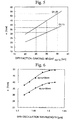
- Fig. 3 is a characteristic diagram showing the relationship between the mask width and the photoluminescence wavelength for explaining the action of the present invention.
- Fig. 4 is a characteristic diagram showing the relationship between the mask width and the photoluminescence wavelength for explaining the action of the present invention.
- Fig. 5 is a characteristic diagram showing the results of theoretical calculation related to the relationship between the diffraction grating height and the coupling coefficient.
- Fig. 6 is a device characteristic diagram showing the relationship between the oscillating wavelength and the coupling coefficient for explaining the action of the present invention.
- Fig. 7 is a diagram showing the crystal growth characteristics for explaining the action of the present invention.
- Fig. 8 is a diagram showing the crystal growth characteristics for explaining the action of the present invention.
- Fig. 9 is a diagram showing the device characteristics for explaining the action of the present invention.
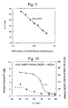
- Fig. 10 is a diagram showing the device characteristics for explaining the action of the present invention.
- Fig. 11 is a diagram showing the device characteristics for explaining the action of the present invention.
- Fig. 12 is a characteristic diagram showing the results of theoretical calculations as a parameter of the diffraction grating height for explaining the action of the present invention.
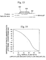
- Fig. 13 is a cross-sectional view of a crystal growing apparatus for explaining the action of the present invention.
- Fig. 14 is a characteristic diagram showing the crystal growth characteristics for explaining the action of the present invention.
- Figs. 15A and 15B are perspective views showing manufacturing processes according to one embodiment of the present invention.
- Fig. 16 is a plan view showing a manufacturing process according to one embodiment of the present invention.
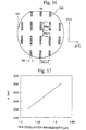
- Fig. 17 is a diagram showing the theoretical characteristics of one embodiment of the present invention.
- Fig. 18 is a plan view showing the substrate surface for explaining one embodiment of the present invention.
- Fig. 19 is a characteristic diagram explaining one embodiment of the present invention.
- Fig. 20 is a plan view explaining one embodiment of the present invention.
- Fig. 21 is a perspective view explaining one embodiment of the present invention.
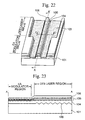
- Fig. 22 is a perspective view explaining one embodiment of the present invention.
- Fig. 23 is a cross-sectional view along the A-A' line in Fig. 22.
- Figs. 24A to 24C are cross-sectional views along the C-C' line in Fig. 22 for explaining the manufacturing processes according to one embodiment of the present invention.
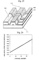
- Fig. 25 is a perspective view explaining one embodiment of the present invention.
- Fig. 26 is a characteristic diagram explaining one embodiment of the present invention.
- Fig. 27 is a characteristic diagram explaining one embodiment of the present invention.
- Fig. 28 is a characteristic diagram explaining one embodiment of the present invention.
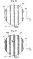
- Fig. 29 is a plan view of a substrate surface explaining one embodiment of the present invention.
- Fig. 30 is a plan view of the substrate surface explaining one embodiment of the present invention.
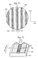
- Fig. 31 is a plan view of the substrate surface explaining one embodiment of the present invention.
- Fig. 32 is a perspective view explaining one embodiment of the present invention.
- Figs. 33A to 33E are cross-sectional views explaining the manufacturing processes according to one embodiment of the present invention.
- Fig. 34 is a perspective view showing the structure of one embodiment of the present invention.
- Fig. 35 is a characteristic diagram explaining one embodiment of the present invention.
- Fig. 36 is a characteristic diagram explaining one embodiment of the present invention.
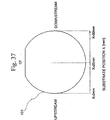
- Fig. 37 is a plan view showing the substrate surface explaining one embodiment of the present invention.
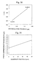
- Fig. 38 is a design characteristic diagram explaining one embodiment of the present invention.
- Fig. 39 is a characteristic diagram explaining one embodiment of the present invention.
- Fig. 40 is a design characteristic diagram explaining one embodiment of the present invention.
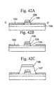
- Fig. 41 is a perspective view explaining one embodiment of the present invention.
- Figs. 42A to 42C are cross-sectional views along the C-C' line in Fig. 41 for explaining one embodiment of the present invention.
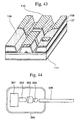
- Fig. 43 is a perspective view explaining one embodiment of the present invention.
- Fig. 44 is a diagram showing the structure of an optical communication module for explaining an application example of the present invention.
- Fig. 45 is a diagram showing an example of the optical communication system for explaining an application example of the present invention.
- Fig. 46 is a perspective view showing an example of the collective formation of a conventional different wavelength element.
- the inventors of the present invention have examined how the mask width and the coupling coefficient ⁇ affect the properties of the present type of optical semiconductor device.
- a series of examinations has revealed an important fact in the relationship between the mask width or the coupling coefficient and the oscillating frequency of the DFB laser. That is, a technique was found by the present inventors to maintain the coupling coefficient constant even if the oscillating frequency changes with each DFB laser.
- several measures were also found for improving the characteristics of this type of optical semiconductor devices.
- Fig. 1 shows a schematic cross-sectional view of an InGaAsP crystal grown by a selective MOVPE method.
- an InGaAsP layer was selectively grown as a selective growing layer 3 by the MOVPE method using a pair of stripe-shaped SiO 2 masks formed in the [011] direction of a crystal plane separated by a space of 1.5 ⁇ m.
- the crystal grows into a trapezoidal form, and the side facet and the top surface of the trapezoid are formed by the (111) B plane and the (100) plane, respectively.
- the growth rate (of the film thickness) is increased by the material supply from the masked region and it is known that the In content in the crystal composition increases. Utilization of this phenomenon makes it possible to produce, in one substrate surface, a plurality of layers respectively having different band-gap wavelengths only by changing mask width.
- Fig. 2 shows a cross-sectional view of the DFB laser in the waveguide axis direction.
- the typical DFB laser structure is formed by first forming a diffraction grating 100 having a constant height d GTG on an InP substrate 101, and laminated layers on the diffraction grating comprising an InGaAsP guide layer 104, a multi-quantum well active layer 105, and an InP clad layer 106.
- a composition having a band-gap wavelength of 1.0 to 1.3 ⁇ m is frequently used as that of the InGaAsP guide layer.
- Fig. 3 shows a relationship between the photoluminescence wavelength and the mask width of the InGaAsP (Q1.13 means InGaAsP which band gap wavelength is 1.13 ⁇ m and Q1.20 means InGaAsP which bandgap wavelength is 1.20 ⁇ m) layers grown by the selective MOVPE with the growth condition of lattice matching to InP at a mask width of 15 ⁇ m.
- the band-gap wavelength is 1.13 ⁇ m (Q is 1.13)
- the photoluminescence wavelength can be extended to 1.20 ⁇ m.
- This extension of wavelength is due to the strain caused by the increase of the In content in the selectively grown layer induced by the increase of the mask width.
- Fig. 4 shows an example of the relationship between the photoluminescence wavelength and the mask width when the MQW structure composed of InGaAsP/InGaAsP is grown by the selective MOVPE.
- the band-gap wavelength can cover a range of wavelengths from 1.52 ⁇ m to 1.62 ⁇ m when the mask width is increased from 15 ⁇ m to 50 ⁇ m.
- the wavelength range of 1.45 ⁇ m to 1.55 ⁇ m can be covered when the mask width is increased from 5 ⁇ m to 21 ⁇ m.
- This wavelength range of 1.45 ⁇ m to 1.55 ⁇ m can be used as an operating wavelength range for the electro-absorption (EA) modulator to be integrated in combination with the above-described DFB laser having an oscillating wavelength range of 1.52 ⁇ m to 1.62 ⁇ m.
- EA electro-absorption
- the issue is the wavelength dependency of the coupling coefficient ⁇ when manufacturing the DFB lasers.
- the photoluminescence wavelength of the guide layer changes from 1.13 ⁇ m to 1.20 ⁇ m.
- the change of the photoluminescence wavelength means a change in the band-gap wavelength induced by the change of the refractive index of the guide layer, which implies that the coupling coefficient ⁇ changes due to the periodic change of the refractive index produced by the diffraction grating.
- Fig. 5 shows the results of the calculation between the height d GTG of the diffraction grating, which has a proportional relationship with the change value of the periodic change of the refractive index, and the coupling coefficient using the composition of the guide layer as a parameter.
- the band-gap wavelength changes with the change of the composition of the guide layer from 1.13 ⁇ m to 1.20 ⁇ m
- the coupling coefficient ⁇ changes from 37.5 to 53 cm -1 .
- Fig. 7 shows an example of the film thickness distribution when the flow rate is increased to 1.5 times higher than the optimum flow rate.
- the growth rate distribution is represented as a function of the normalized growth rate, wherein the growth rate at the center of a 2 inch InP substrate is set at 1, against the distance from the center of the substrate. From the figure, the growth rate at the outermost periphery of the substrate is about 1.4 times larger than that at the center of the substrate.
- PL photoluminescence
- utilization of the structure having the above wavelength distribution makes it possible to execute the collective formation of the DFB lasers having different oscillation wavelengths on one substrate surface. It is possible to produce DFB lasers having a wavelength range of 1.53 ⁇ m to 1.58 ⁇ m by setting the mask width at 16 ⁇ m. The wavelength range of 1.46 ⁇ m to 1.51 ⁇ m can be covered by setting the mask width at 6 ⁇ m, and this wavelength range can be used as the operating wavelength range of the electro-absorption (EA) modulator for DFB lasers having an oscillating wavelength range of 1.53 ⁇ m to 1.58 ⁇ m.
- EA electro-absorption
- the change of the long distance transmission characteristics due to the change of the coupling coefficients ⁇ is originated by the wavelength variation (wavelength chirp) induced by the residual reflection light from the end facet at the time of the modulation operation.
- Fig. 10 shows the relationship between the coupling coefficients ⁇ and the power penalty after a 2.5 Gb/s modulated transmission over 600 km (indicated by broken line ⁇ ).
- the measurement was made using a device produced by monolithic integration of a 400 ⁇ m long uniform diffraction grating-type DFB laser with a 200 ⁇ m long EA modulator.
- the power penalty after transmission over 600 km decreases with an increase of the coupling coefficients ⁇ , and a power penalty less than 1 dB is obtained when the coupling coefficients ⁇ >37 cm -1 .
- the relationship (the real line ⁇ ) between the coupling coefficient ⁇ and the longitudinal single mode oscillation yield shows that the yield is reduced by the larger effect of the spatial hole burning as the coupling coefficient ⁇ increases. Therefore, it is very important to control the coupling coefficient ⁇ to within a certain range.
- Fig. 11 shows a similar relationship between the power penalty and the product ⁇ L of the coupling coefficient ⁇ and the DFB laser oscillator length L and the product ⁇ L must be more than 1.5 in order to obtain a power penalty less than 1 dB.
- the elements integrated in the multiple wavelength laser necessarily involve the change of the coupling coefficient ⁇ , since each laser active layer structure (composition or film thickness) differs from each other in order to provide elements having different wavelengths.
- the coupling coefficient ⁇ can be controlled not only by the change of the height of the diffraction grating but also by the composition of the guide layer (band-gap wavelength) on the diffraction grating, as shown in Fig. 5. That is, the change of the coupling coefficient ⁇ can be cancelled by controlling the band-gap wavelength of the guide layer on the diffraction grating independent from the MQW structure which determines the band-gap wavelength of the laser active layer.
- Fig. 12 shows the results of the calculation regarding the relationship between the band-gap wavelength and the coupling coefficient ⁇ when changing the height of the diffraction grating as parameters.
- the calculation is carried out based on the MQW structure of the DFB laser with an oscillating wavelength of 1.52 ⁇ m, whose coupling coefficient ⁇ dependent on the oscillating wavelength is shown in Fig. 9.
- the coupling coefficient ⁇ increases into two times from 37.5 cm -1 to 75 cm -1 when the band-gap wavelength is varied from 1.13 ⁇ m to 1.30 ⁇ m.
- the coupling coefficient ⁇ is reduced to 50% for elements having wavelengths from 1.52 ⁇ m to 1.58 ⁇ m
- the first method is to form the guide layer on the diffraction grating and the MQW active layer by respective selective MOVPEs. It is possible to change the band-gap wavelength (photoluminescence wavelength) from 1.12 ⁇ m to 1.30 ⁇ m within a mask width of 2 to 50 ⁇ m when the InGaAsP layer having the band-gap wavelength of 1.20 ⁇ m (Q1.20) is grown by the selective MOVPE at the mask width of 15 ⁇ m under the lattice matching condition.
- the second method is to grow the guide layer under intentionally non-homogeneous growing condition using an atmospheric pressure double fluid layer flow-type MOVPE.
- an atmospheric pressure double fluid layer flow-type MOVPE is disclosed in detail in The Journal of Crystal Growth, 145, p. 622, 1994, the principle is briefly described below with reference to Fig. 13.
- the reaction tube 501 of the atmospheric pressure double fluid layer flowing-type MOVPE reactor has a material inlet, which is divided into two upper and lower layer-shaped inlets with respect to the semiconductor substrate 503 supported by the substrate holder 502, as shown in Fig. 13.
- the reaction tube 501 is constituted such that arsine (AsH 3 ) and phosphine (PH 3 ), which belongs to Group V, are supplied from the upper layer-shaped inlet located near the substrate' and the materials, which belongs to Group III such as trimethylgallium (TMGa), or trimethylindium (TMIn), are supplied from the lower layer-shaped inlet located far from the substrate.
- the reason it is difficult to carry out the homogeneous growth of the InGaAsP by the MOVPE growth is that the existing ratio of As and P atoms differs on the substrate surface due to the large difference in the decomposition rate constants of AsH 3 and PH 3 (the decomposition rate of AsH 3 is about ten times larger than that of PH 3 t a growth temperature of 600 to 650°C).
- this MOVPE growth is characterized in that PH 3 having a small decomposition rate constant, is supplied from the upper layer-shaped inlet located close to the substrate, and AsH 3 is supplied from both upper and lower inlets such that the homogeneous growth of the InGaAsP is attained by conforming the numbers of As atoms with P atoms reaching the substrate surface by adjusting the AsH 3 flow rate of the upper inlet and the lower inlet.
- Fig. 14 shows an example.
- Q1.25 InGaAsP having a composition corresponding to the band-gap wavelength of 1.25 ⁇ m
- a method for collective manufacturing the different wave EA modulator integrated-type DFB laser according to the first embodiment of the present invention is described.
- a pattern, as shown in Fig. 15A is formed by electron-beam exposure.
- a diffraction grating as shown in Fig. 15B, is formed by etching the n-InP substrate 101 with an HBr: H 2 O-type etching solution using the resist 102 as the mask.
- the diffraction grating is formed as a pattern, in which a diffraction grating formation region with a length of 800 ⁇ m in the [011] direction and a non-diffraction grating formation region with a length of 400 ⁇ m are repeatedly formed in the [01-1] direction.
- the pitch ⁇ of the diffraction grating is set within a range of 235.05 to 244.30 nm which can yields oscillating waveelengths ranging from 1.52 to 1.58 ⁇ m.
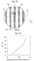
- a pair of stripe masks 103g made of SiO 2 for forming a guide layer on the diffraction grating by the selective MOPVE growth is obtained by patterning as shown in Fig. 18.
- the relationship between the width W G of the SiO 2 mask for the selective MOPVE growth and the DFB laser oscillating wavelength is shown in Fig. 19.
- the width W G is characterized in being set larger as the DFB oscillating wavelength increases to a longer wavelength, wherein the coupling coefficient ⁇ becomes smaller, as shown in Fig. 9.
- a pair of SiO 2 masks used for the selective MOPVE growth is re-patterned so as to be synchronous with the diffraction grating 100.
- the mask width is set at W LD in the region wherein the diffraction grating is formed, and the mask width is set at W MOD in the region wherein no diffraction grating is formed.
- the n-Q1.20 guide layer is formed in the aperture region where no diffraction grating is formed, as explained in Figs. 18 and 19.
- Fig. 21 illustrates the SiO 2 mask pattern for one element (the n-Q1.20 guide layer is not shown in this figure). That is, the region where the mask width is set at W LD (400 ⁇ m in length) is used for forming the DFB laser, and the region where the mask width is set at W MOD (200 ⁇ m in length) is used for forming the EA modulator.
- the space between one pair of SiO 2 stripe masks is fixed at 1.5 ⁇ m.
- the W LD is fixed at 16 ⁇ m and the W MOD is set at 6 ⁇ m.
- Figs. 17 and 19 the pitch A and the width W G of the diffraction grating are shown to have a continuous relationship with the oscillating frequencies. However, in this embodiment, since the range of the oscillating wavelengths 1.52 ⁇ m to 1.58 ⁇ m are divided into 75 wavelengths by an interval of 100 GHz (approximately 0.8 nm), the actual lines in Figs. 17 and 19 are actually composed of 75 discontinuous dots.
- the MQW laser active layer and the modulator absorption layer are grown by the selective MOVPE growth.
- the crystal growth by the selective MOVPE growth is carried out under conditions so as to provide a film having the thickness distribution as shown in Fig. 7.
- Fig. 23 which is a cross-sectional view along the A-A'line shown in Fig. 22, the diffraction grating is present in the DFB laser region.
- Fig. 24 which is a cross-sectional view along the C-C' line shown in Fig. 22
- a p-type electrode 110 is formed by patterning using the SiO 2 film 109 as the interlayer insulating film, and an n-type electrode 111 is formed after back grinding is carried out until the thickness of the n-InP substrate is reduced to 120 ⁇ m.
- a total length of 600 ⁇ m of the thus formed substrate including the DFB laser portion of 400 ⁇ m in length and the EA modulator portion of 200 ⁇ m in length is cut into elements. Each element is subjected to the evaluation of the device characteristics after coating a high reflection film with a reflectance of 95% at the end facet of the DFB laser portion and after coating an anti-reflection film with less than 0.1% reflectance at the end facet of the modulator.
- DFB laser oscillating wavelengths of the 75 thus produced elements are plotted in Fig. 26 in sequence. It is confirmed that the wavelengths of these elements from channel 1 to channel 75 are shifted from one to the next channel by 0.8 nm as intended and multiple wavelength laser elements covering the wavelength range of 1520 to 1580 nm (1.52 to 1.58 ⁇ m) are provided on one substrate surface.
- the coupling coefficients ⁇ for some elements having different wavelengths are evaluated. Consequently, it has been confirmed, as shown in Fig. 27, that the coupling coefficient is maintained approximately at a designed value of 37.5 cm -1 irrespective of the change of the oscillating wavelength.
- This result is obtained by utilizing the effect of the present invention that the band-gap wavelengths of the InGaAsP guide layers for respective elements on the diffraction grating are changed corresponding to the oscillating wavelengths of the elements.
- the transmission yield obtained by use of a standard that the power penalty after 2.5 Gb/s transmission over 600 km is less than 1dB, is more than 95% in all wavelength ranges, while the single longitudinal mode oscillation yield is maintained to more than 60% irrespective of the oscillation wavelength.
- the diffraction grating is formed by electron beam exposure and etching. As shown in Fig. 29, the diffraction grating is formed on the entire region of the [01-1] direction, and a repeating pattern is formed t a pitch of 300 ⁇ m in the [01-1] direction.
- the diffraction grating pitch ⁇ is controlled from 235.05 to 244.30 nm in order to control the DFB oscillating wavelengths to within a range of 1.52 ⁇ m to 1.58 ⁇ m, corresponding to the DFB oscillating wavelength.
- the etching amount shown in Fig. 15B is controlled so as to obtain a grating height of 30 nm.
- a plurality of SiO 2 stripe masks 203g are formed by the patterning process for growing the guide layer on the diffraction grating 200 by the MOVPE growth.
- the mask width is represented by W G .
- the relationship shown in Fig. 19, between the mask width W G for forming the guide layer by the MOVPE growth and the oscillating frequencies of the DFB lasers is used for forming the SiO 2 masks.
- the microscopic photoluminescence measurement of the band-gap wavelength of the selective grown guide layer clearly shows that the mask width dependence on the band-gap wavelengths has been reproduced as shown in Fig. 3.
- a pair of SiO 2 stripe masks for growing the MQW active layer by the selective MOVPE growth method is formed by re-patterning so as to synchronize with the diffraction grating.
- the n-Q1.20 guide layer is present in the aperture region of the SiO 2 stripes.
- Fig. 32 illustrates a SiO 2 mask pattern for one element (the n-Q1.20 guide layer is not shown in this figure).
- the interval of the pair of stripe masks is fixed at 1.5 ⁇ m.
- the pitches A and W G of the diffraction grating are shown continuously as lines in Figs. 17 and 19, the pitches of the present embodiment are cut into 75 wavelengths by dividing the wavelength range of 1.52 ⁇ m to 1.58 ⁇ m into 75 steps with the interval of 100GHz (approximately 0.8 nm), so that it is noted that the lines in Figs. 17 and 19 are composed of 75 steps of discontinuous values.
- Fig. 33 is a cross-sectional view of the D-D' line shown in Fig. 32.
- the MOVPE growth is conducted under a condition such that the film is grown with a thickness distribution as shown in Fig. 7.
- a p-InP block layer 208, an n-InP block layer 209, and a p-InP layer 210 are selectively grown as shown in Fig. 33D.
- a p-InP clad layer 211 and a p + -InGaAs cap layer 212 are grown by the selective MOVPE growth method.
- a p electrode 214 is formed by patterning using the SiO 2 film as an interlayer insulating film, and after back-grinding of the n-InP substrate 201 until obtaining a thickness of 100 ⁇ m, an n-type electrode 215 is formed on the back surface.
- an element is obtained by cutting the substrate 210 into a length of 400 ⁇ m, and characteristics of the element are evaluated by coating a high reflectance film having a 95% reflectance on the one end facet of the DFB laser and coating a non-reflectance film having a reflectance of 0.1% on the other end facet.
- the oscillating wavelengths of the DFB laser composed of 75 elements are shown in Fig. 26.
- the wavelengths of respective elements from channel 1 to channel 75 are shifted stepwise to longer wavelengths by a slope of 0.8 nm/channel, and it is confirmed that different wavelength elements are provided on one substrate covering a range of 1520 to 1580 nm (1.52 to 1.58 ⁇ m).
- the coupling coefficient ⁇ of these laser elements are examined.
- an electron beam sensitive positive resist 102 is coated on the (100) n-InP substrate 101, and the pattern shown in Fig. 15A is formed.
- the diffraction grating shown in Fig. 15A is formed by etching the n-InP substrate 101 using an etching solution in the system of HBr:H 2 O using of the resist 102 as the mask.
- the diffraction grating is formed as a pattern in which a diffraction grating formation region with a length of 800 ⁇ m in the [011] direction and a non-diffraction grating formation region with a length of 400 ⁇ m are repeatedly formed in the [01-1] direction.
- the pitch ⁇ of the diffraction grating is set within a range of 235.05 to 244.30 nm which can yield oscillating wavelengths ranging from 1.52 to 1.58 ⁇ m.
- the arrangement of this different pitch in the diffraction grating is explained with reference to Figs. 37 and 38.
- the position coordinate of the 2 inch InP substrate is defined in Fig. 37.
- the AsH 3 partial flow ratio is set at 85%.
- Fig. 39 shows the substrate position dependence of the photoluminescence wavelength formed by the above-described two layer-type MOVPE growth.
- a pair of SiO 2 stripe masks for the selective MOVPE growth is re-patterned as shown in Fig. 20 so as to synchronize with the diffraction grating 100.
- the mask width is set at W LD in the region where the diffraction grating is formed, and the mask width is set at W MOD in the region where the diffraction grating is not formed.
- the n-Q1.25 guide layer is formed on the entire substrate surface.
- Fig. 21 shows the SiO 2 stripe mask pattern for one element (the n-Q1.25 guide layer is also not shown in Fig. 21). That is, the area (400 ⁇ m in length) where the mask width is formed at W LD is the region for forming the DFB laser, and the area (200 ⁇ m length) where the mask width is formed at W MOD is the region for forming the EA modulator.
- the width of a pair of stripe masks is fixed at 1.5 ⁇ m.
- the widths of W LD and W MOD are varied corresponding to the DFB oscillating wavelength as shown in Fig. 40.
- the relationship between the pitches ⁇ including W LD and W MOD of the diffraction grating and the DFB oscillating wavelength are depicted as two straight lines, it is noted that these lines consist of 75 discontinuous values corresponding to the design values obtained by dividing the DFB oscillating wavelength range of 1.52 to 1.58 ⁇ m by 100 GHz (approximately 0.8 nm intervals).
- a MQW laser active layer and a modulator absorption layer are formed using the selective MOVPE growth method.
- the photoluminescence wavelengths in the range of 1.52 to 1.58 ⁇ m and in the range of 1.45 to 1.51 ⁇ m are reproduced for respective widths of W LD and W MOD as shown in Fig. 4.
- the diffraction grating exists in the DFB laser region.
- the bandgap wavelength of the guide layer 104 changes from 1.17 ⁇ m to 1.25 ⁇ m as designed.
- the coupling coefficient ⁇ is expected to be maintained at a fixed value of 37.5 cm -1 .
- electrical separation is performed by removing the p + -InGaAs cap layer 108 with a width of 30 ⁇ m between the DFB laser region and the EA modulator region.
- a p-type electrode 110 is formed by patterning using the SiO 2 film 109 as the interlayer insulating film, and an n-type electrode 111 is formed after back grinding is carried out until the thickness of the n-InP substrate is reduced to 120 ⁇ m.
- Each element is subjected to the evaluation of the device characteristics after coating a high reflection film with a reflectance of 95% at the end facet of the DFB laser portion and after coating an anti-reflection film with less than 0.1% reflectance at the end facet face of the modulator.
- the oscillating wavelength characteristics of this different wavelength collectively formed EA modulator integrated DFB laser are examined.
- the DFB laser oscillating wavelengths of the 75 thus produced elements are plotted in Fig. 26 in sequence. It is confirmed that the wavelengths of these elements from channel 1 to channel 75 are shifted to longer wavelengths from one to the next channel by 0.8 nm as designed and multiple wavelength laser elements covering the wavelength range of 1520 to 1580 nm (1.52 to 1.58 ⁇ m) are provided on one substrate surface.
- the coupling coefficients ⁇ for some elements having different wavelengths are evaluated. Consequently, it has been confirmed as shown in Fig. 27 that the coupling coefficient is maintained approximately at the designed value of 37.5 cm -1 irrespective of the change of the oscillating wavelength.
- This result is obtained by utilizing the effect of the present invention that the band-gap wavelengths of the InGaAsP guide layers for respective elements on the diffraction grating are changed corresponding to the oscillating wavelengths of the elements.
- the transmission yield obtained by use of a standard that the power penalty after the 2.5 Gb/s transmission over 600 km is less than 1dB, is more than 95% in all wavelength ranges, while the single longitudinal mode oscillation yield is maintained to more than 60% irrespective of the oscillation wavelength.
- a light communication module provided with an optical semiconductor device is described with reference to Fig. 44.
- This module loaded with an electric interface 301 for driving the optical semiconductor device 302, is constituted such that the output light from the optical semiconductor device 302 is input into the optical fiber 305 through an aspherical lens and an optical isolator.
- This module constituted as described above, makes it possible to effectively execute high speed optical transmission. This effect is obtained through the low threshold value and highly efficient operating characteristics of the optical semiconductor device of the present invention.
- the optical communication apparatus 400 comprises 64 optical communication modules 300, a multiplexer 405 for multiplexing multiple lights from these light emitting elements in the optical communication module 300, and a driving system 402 for driving the light transmission module.
- a signal light output from the optical communication apparatus 400 is transmitted to the optical receiving apparatus 401 through the optical fiber 305.
- the light having 64 wavelengths which is received by the optical receiving apparatus is divided into 64 light signals by the optical demultiplexer 406 and each divided light signal is input into each of 64 light receiving modules 403, driven by the receiving module driving system 404.
- the WDM communication system is realized by the optical communication system of the present invention. This is due to the fact that the optical semiconductor device has quite homogeneous characteristics irrespective of the variation of the wavelengths.
- the optical semiconductor device and method for manufacturing the same according to the present invention is constituted as described above.
- the manufacturing method for collectively manufacturing the multiple wavelength DFB laser or the multiple wavelength EA modulator integrated DFB laser is capable of maintaining the coupling coefficients ⁇ of respective elements by controlling the refractive index (the band-gap wavelength) of the guide layer corresponding to the dielectric material mask width or the location on the substrate. Thereby, it becomes possible to maintain the coupling coefficient ⁇ or the product ⁇ L of the coupling coefficient and the length of the DFB laser resonator, which results in an improvement in the long distance transmission yield or the longitudinal single mode oscillation yield.
Landscapes
- Physics & Mathematics (AREA)
- Condensed Matter Physics & Semiconductors (AREA)
- General Physics & Mathematics (AREA)
- Electromagnetism (AREA)
- Optics & Photonics (AREA)
- Semiconductor Lasers (AREA)
- Optical Modulation, Optical Deflection, Nonlinear Optics, Optical Demodulation, Optical Logic Elements (AREA)
Abstract
Description
Claims (18)
- An optical semiconductor device comprising a plurality of semiconductor lasers formed on a single substrate, wherein each of said semiconductor lasers emits laser lights having oscillating wavelengths differing from each other by different cycles of a plurality of diffraction gratings, wherein a composition of an optical guide layer in contact with one of said diffraction gratings is determined such that the coupling coefficient of each of said semiconductor lasers is maintained at the same value.
- An optical semiconductor device comprising a plurality of semiconductor lasers formed on a single substrate, wherein each of said plurality of semiconductor lasers emits longitudinal single mode laser lights having different oscillating wavelengths due to a distributed feedback operation of a periodic change of the refractive index in said plurality of semiconductor lasers and wherein said plurality of semiconductor lasers have the same coupling coefficient by being provided with a diffraction grating embedded semiconductor layer each having a refractive index corresponding to the oscillating wavelength.
- An optical semiconductor device according to claim 1, wherein said semiconductor laser is a distributed feedback semiconductor laser.
- An optical semiconductor device according to claim 1, wherein each of said plurality of diffraction gratings has the same height.
- An optical semiconductor device according to claim 1, wherein each of said plurality of semiconductor lasers comprises a diffraction grating embedded semiconductor layer made of InGaAsP having a band-gap wavelength (energy) corresponding to the oscillating wavelength thereof.
- An optical semiconductor device according to claim 1, wherein said substrate is made of InP, said diffraction gratings are formed to the same height from said substrate, and said optical guide layer is made of InGaAsP formed on said diffraction gratings.
- An optical semiconductor device according to claim 1, wherein an optical modulator is monolithically integrated with said semiconductor laser.
- An optical semiconductor device comprising a plurality of semiconductor lasers provided with a plurality of diffraction gratings having cycles different from each other, an InGaAsP guide layer formed on or below said diffraction gratings, a multi-quantum well layer, and an InP clad layer on an InP substrate, and which emit laser lights having different wavelengths determined by the cycle of said diffraction gratings, wherein the refractive index of said guide layer is adjusted so as to equalize the coupling coefficients of the respective semiconductor lasers.
- A manufacturing method for collectively manufacturing, on a single substrate, an optical semiconductor device comprising a plurality of semiconductor lasers which emit longitudinal single mode laser lights having different wavelengths due to a distribution feedback operation of a periodic change of the refractive indexes in the respective semiconductor lasers, wherein the refractive indexes of diffraction grating embedded semiconductor layers are decreased (or increased) so as to cancel the difference of the coupling coefficients of respective semiconductor lasers whose coupling coefficients are increased (or decreased) when the diffraction gratings for generating a distribution feedback operation are formed in the same configuration and the refractive indexes of said diffraction grating embedded semiconductor layers are fixed at the same value.
- A manufacturing method for collectively manufacturing, on a single substrate, an optical semiconductor integrated device comprising a plurality of semiconductor lasers which emit longitudinal single mode laser lights having different wavelengths due to a distributed feedback operation of a periodic change of the refractive indexes in the respective semiconductor lasers, and a plurality of optical semiconductor portions integrally formed with said semiconductor lasers for receiving the respective laser lights from said plurality of semiconductor lasers, wherein the refractive indexes of said diffraction grating embedded semiconductor layers are decreased (or increased) so as to cancel the difference of the coupling coefficients of respective semiconductor lasers for the semiconductor lasers whose coupling coefficient is increased (or decreased) when the diffraction gratings for generating a distributed feedback operation are formed in the same configuration and the refractive indexes of the diffraction grating embedded semiconductor layers are fixed at the same value.
- A manufacturing method according to claim 10, wherein said optical semiconductor integrated device comprises longitudinal single mode oscillating semiconductor lasers and optical modulators.
- A manufacturing method according to claim 9, wherein the band-gap wavelengths of said diffraction grating embedded semiconductor layers are made shorter (or longer) so as to cancel the difference of the coupling coefficients of the respective semiconductor lasers for the semiconductor lasers whose coupling coefficients are increased (or decreased) when the diffraction gratings for generating a distributed feedback operation are formed in the same configuration and the band-gap wavelengths of said diffraction grating embedded semiconductor layers are fixed at the same value.
- A manufacturing method according to claim 12, wherein said diffraction grating embedded semiconductor layer is made of InGaAsP, and the change of the refractive index of said InGaAsP layer is executed by changing the compositional ratio of In and Ga in Group III in the periodic table .
- A manufacturing method according to claim 12, wherein said diffraction grating embedded semiconductor layer is made of InGaAsP, and the change of the band-gap wavelength is executed by changing the compositional ratio of As and P belonging to Group V of the periodic table.
- A manufacturing method according to claim 9, wherein the method for changing the refractive index or the band-gap wavelength of said diffraction grating embedded semiconductor layer is a selective metal organic vapor phase growth method.
- A manufacturing method according to claim 9, wherein the method for changing the refractive index or the band-gap wavelength of said diffraction grating embedded semiconductor layer is provided by adjusting a flowing ratio of Group V materials in an atmospheric pressure double fluid layer type metal organic vapor phase growth method.
- An optical semiconductor device according to claim 1 or the semiconductor device obtained by the manufacturing method according to claim 16 which is applied to an optical communication module, wherein the optical communication module comprises: a waveguide device for guiding an output light from said optical semiconductor device to the outside, a mechanism for inputting the output light from said semiconductor device to the waveguide device, and an electrical interface for driving said semiconductor device.
- An optical semiconductor device according to claim 17, wherein said semiconductor device according to claim 1 or the semiconductor device obtained by the manufacturing method according to claim 16 is applied to an optical communication apparatus, which comprises an optical transmission device provided with said optical communication module and a receiving device for receiving the output light from said light transmission device.
Applications Claiming Priority (2)
| Application Number | Priority Date | Filing Date | Title |
|---|---|---|---|
| JP2000050248A JP3339488B2 (en) | 2000-02-25 | 2000-02-25 | Optical semiconductor device and method of manufacturing the same |
| JP2000050248 | 2000-02-25 |
Publications (3)
| Publication Number | Publication Date |
|---|---|
| EP1130706A2 true EP1130706A2 (en) | 2001-09-05 |
| EP1130706A3 EP1130706A3 (en) | 2002-10-16 |
| EP1130706B1 EP1130706B1 (en) | 2005-01-19 |
Family
ID=18572054
Family Applications (1)
| Application Number | Title | Priority Date | Filing Date |
|---|---|---|---|
| EP01400483A Expired - Lifetime EP1130706B1 (en) | 2000-02-25 | 2001-02-23 | Optical semiconductor device and method for manufacturing the same |
Country Status (3)
| Country | Link |
|---|---|
| US (2) | US20010019568A1 (en) |
| EP (1) | EP1130706B1 (en) |
| JP (1) | JP3339488B2 (en) |
Cited By (1)
| Publication number | Priority date | Publication date | Assignee | Title |
|---|---|---|---|---|
| EP1283572A3 (en) * | 2001-08-10 | 2004-01-07 | The Furukawa Electric Co., Ltd. | Semiconductor laser device having improved output power characteristics |
Families Citing this family (19)
| Publication number | Priority date | Publication date | Assignee | Title |
|---|---|---|---|---|
| JP2001320124A (en) * | 2000-05-09 | 2001-11-16 | Nec Corp | Modulator integrated light source and module for optical communication |
| DE60238195D1 (en) * | 2001-05-31 | 2010-12-16 | Nichia Corp | SEMICONDUCTOR LASER ELEMENT |
| US7024067B2 (en) * | 2001-10-19 | 2006-04-04 | Visteon Global Technologies, Inc. | Communication system with a signal conduction matrix and surface signal router |
| US6949758B2 (en) * | 2001-10-19 | 2005-09-27 | Visteon Global Technologies, Inc. | LCC-based fluid-level detection sensor |
| US6772733B2 (en) | 2001-10-19 | 2004-08-10 | Visteon Global Technologies, Inc. | Optically controlled IPCS circuitry |
| US20030090161A1 (en) * | 2001-10-19 | 2003-05-15 | Marlow C. Allen | Light communication channel-based electronics power distribution system |
| JP3912117B2 (en) * | 2002-01-17 | 2007-05-09 | ソニー株式会社 | Crystal growth method, semiconductor light emitting device and method for manufacturing the same |
| US20050053109A1 (en) * | 2002-06-03 | 2005-03-10 | Josh Hogan | Integrated multiple wavelength system |
| KR100852110B1 (en) * | 2004-06-26 | 2008-08-13 | 삼성에스디아이 주식회사 | Organic electroluminescent device and manufacturing method thereof |
| GB2430548B (en) * | 2005-09-27 | 2011-08-10 | Agilent Technologies Inc | An integrated modulator-laser structure and a method of producing same |
| JP4552894B2 (en) * | 2006-05-12 | 2010-09-29 | 住友電気工業株式会社 | Method for fabricating distributed feedback semiconductor laser |
| JP5211728B2 (en) * | 2007-02-07 | 2013-06-12 | 住友電気工業株式会社 | Method for fabricating a semiconductor optical device |
| US7539228B2 (en) * | 2007-06-26 | 2009-05-26 | Avago Technologies Fiber Ip (Singapore) Pte. Ltd. | Integrated photonic semiconductor devices having ridge structures that are grown rather than etched, and methods for making same |
| JP5151674B2 (en) * | 2008-05-19 | 2013-02-27 | 信越半導体株式会社 | Epitaxial wafer manufacturing method |
| WO2011146944A2 (en) * | 2010-05-21 | 2011-11-24 | Kaiam Corp. | Mems-based levers and their use for alignment of optical elements |
| JP2014096458A (en) * | 2012-11-08 | 2014-05-22 | V Technology Co Ltd | Optical interconnection device |
| JP6220614B2 (en) * | 2013-09-20 | 2017-10-25 | ルネサスエレクトロニクス株式会社 | Semiconductor device manufacturing method and semiconductor device |
| JP6291849B2 (en) * | 2014-01-10 | 2018-03-14 | 三菱電機株式会社 | Semiconductor device manufacturing method, semiconductor device |
| JP2023019284A (en) * | 2021-07-29 | 2023-02-09 | 日本電信電話株式会社 | Semiconductor optical device |
Family Cites Families (15)
| Publication number | Priority date | Publication date | Assignee | Title |
|---|---|---|---|---|
| US4791647A (en) | 1986-06-17 | 1988-12-13 | Nec Corporation | Semiconductor laser |
| JPH088394B2 (en) | 1989-06-30 | 1996-01-29 | 三菱電機株式会社 | Semiconductor laser and manufacturing method thereof |
| JPH05110187A (en) * | 1991-10-15 | 1993-04-30 | Matsushita Electric Ind Co Ltd | Array type semiconductor laser and manufacturing method thereof |
| JP3306892B2 (en) * | 1992-02-28 | 2002-07-24 | 株式会社日立製作所 | Semiconductor optical integrated device and method of manufacturing the same |
| JPH06120906A (en) | 1992-10-03 | 1994-04-28 | Canon Inc | Optical receiver, optical semiconductor device, optical communication system and optical communication system using the same |
| EP0606093B1 (en) * | 1993-01-07 | 1997-12-17 | Nec Corporation | Semiconductor optical integrated circuits and method for fabricating the same |
| JP3611593B2 (en) * | 1994-02-14 | 2005-01-19 | 日本オプネクスト株式会社 | Method for fabricating semiconductor optical device |
| JPH08292336A (en) * | 1995-04-20 | 1996-11-05 | Nec Corp | Production of optical semiconductor integrated circuit |
| US5668900A (en) | 1995-11-01 | 1997-09-16 | Northern Telecom Limited | Taper shapes for sidelobe suppression and bandwidth minimization in distributed feedback optical reflection filters |
| JP3714430B2 (en) * | 1996-04-15 | 2005-11-09 | シャープ株式会社 | Distributed feedback semiconductor laser device |
| JPH1098235A (en) * | 1996-08-01 | 1998-04-14 | Pioneer Electron Corp | Non-regrowth distribution feedback ridge type semiconductor laser and its manufacture |
| JPH10117040A (en) * | 1996-10-08 | 1998-05-06 | Nec Corp | Semiconductor laser device and method of manufacturing the same |
| EP0952470A3 (en) * | 1998-04-23 | 2004-01-14 | Nec Corporation | A method of manufacturing a semiconductor optical waveguide array and an array-structured semiconductor optical device |
| JP2000312054A (en) * | 1998-04-28 | 2000-11-07 | Sharp Corp | Method of manufacturing semiconductor element and semiconductor element |
| JP3977920B2 (en) | 1998-05-13 | 2007-09-19 | 富士通株式会社 | Manufacturing method of semiconductor device |
-
2000
- 2000-02-25 JP JP2000050248A patent/JP3339488B2/en not_active Expired - Fee Related
-
2001
- 2001-02-23 US US09/790,651 patent/US20010019568A1/en not_active Abandoned
- 2001-02-23 EP EP01400483A patent/EP1130706B1/en not_active Expired - Lifetime
-
2003
- 2003-02-25 US US10/372,278 patent/US6828589B2/en not_active Expired - Fee Related
Cited By (1)
| Publication number | Priority date | Publication date | Assignee | Title |
|---|---|---|---|---|
| EP1283572A3 (en) * | 2001-08-10 | 2004-01-07 | The Furukawa Electric Co., Ltd. | Semiconductor laser device having improved output power characteristics |
Also Published As
| Publication number | Publication date |
|---|---|
| US20030160249A1 (en) | 2003-08-28 |
| JP2001244576A (en) | 2001-09-07 |
| US20010019568A1 (en) | 2001-09-06 |
| US6828589B2 (en) | 2004-12-07 |
| EP1130706A3 (en) | 2002-10-16 |
| JP3339488B2 (en) | 2002-10-28 |
| EP1130706B1 (en) | 2005-01-19 |
Similar Documents
| Publication | Publication Date | Title |
|---|---|---|
| EP1130706B1 (en) | Optical semiconductor device and method for manufacturing the same | |
| EP0546706B1 (en) | Article comprising a DFB semiconductor laser | |
| US6743648B2 (en) | Method for fabricating a set of distributed feedback semiconductor lasers | |
| US8184671B2 (en) | Semiconductor optical element, semiconductor laser using the semiconductor optical element, and optical transponder using the semiconductor laser | |
| US5790580A (en) | Semiconductor optical integrated device | |
| US6399404B2 (en) | Fabricating method of optical semiconductor device | |
| EP0680119B1 (en) | Fabrication process for semiconductor optical device | |
| CN1945365B (en) | Buried heterostructure device fabricated by single step MOCVD | |
| US5539766A (en) | Distributed feedback semiconductor laser | |
| US7949020B2 (en) | Semiconductor laser and optical integrated semiconductor device | |
| EP1104060B1 (en) | Optical semiconductor device and process for producing the same | |
| CN105140779B (en) | Backup semiconductor laser based on reconstruction-equivalent chirp technique | |
| US20010005391A1 (en) | Laser elements having different wavelengths formed from one semiconductor substrate | |
| US5756373A (en) | Method for fabricating optical semiconductor device | |
| JP2000031595A (en) | Optical semiconductor element as well as method and apparatus for manufacture of optical semiconductor element | |
| JP2763090B2 (en) | Semiconductor laser device, manufacturing method thereof, and crystal growth method | |
| JP2001326414A (en) | Optical semiconductor device and its manufacturing method | |
| JPH06283802A (en) | Semiconductor laser device and fabrication thereof | |
| Piataev et al. | Strain-compensated MQW InGaAsP/InGaAsP gain-and index-coupled laser arrays grown by MOVPE under N/sub 2 | |
| Moore et al. | Recent developments in distributed feedback and distributed Bragg reflector lasers for wide-band long-haul fiber-optic communication systems | |
| Sasaki et al. | Selective Growth Techniques and Their Application in WDM Device Fabrication |
Legal Events
| Date | Code | Title | Description |
|---|---|---|---|
| PUAI | Public reference made under article 153(3) epc to a published international application that has entered the european phase |
Free format text: ORIGINAL CODE: 0009012 |
|
| AK | Designated contracting states |
Kind code of ref document: A2 Designated state(s): AT BE CH CY DE DK ES FI FR GB GR IE IT LI LU MC NL PT SE TR |
|
| AX | Request for extension of the european patent |
Free format text: AL;LT;LV;MK;RO;SI |
|
| PUAL | Search report despatched |
Free format text: ORIGINAL CODE: 0009013 |
|
| AK | Designated contracting states |
Kind code of ref document: A3 Designated state(s): AT BE CH CY DE DK ES FI FR GB GR IE IT LI LU MC NL PT SE TR |
|
| AX | Request for extension of the european patent |
Free format text: AL;LT;LV;MK;RO;SI |
|
| RAP1 | Party data changed (applicant data changed or rights of an application transferred) |
Owner name: NEC COMPOUND SEMICONDUCTOR DEVICES, LTD. |
|
| 17P | Request for examination filed |
Effective date: 20030310 |
|
| 17Q | First examination report despatched |
Effective date: 20030508 |
|
| AKX | Designation fees paid |
Designated state(s): FR IT |
|
| REG | Reference to a national code |
Ref country code: DE Ref legal event code: 8566 |
|
| GRAP | Despatch of communication of intention to grant a patent |
Free format text: ORIGINAL CODE: EPIDOSNIGR1 |
|
| GRAS | Grant fee paid |
Free format text: ORIGINAL CODE: EPIDOSNIGR3 |
|
| GRAA | (expected) grant |
Free format text: ORIGINAL CODE: 0009210 |
|
| AK | Designated contracting states |
Kind code of ref document: B1 Designated state(s): FR IT |
|
| PGFP | Annual fee paid to national office [announced via postgrant information from national office to epo] |
Ref country code: FR Payment date: 20050223 Year of fee payment: 5 |
|
| REG | Reference to a national code |
Ref country code: IE Ref legal event code: FG4D |
|
| PLBE | No opposition filed within time limit |
Free format text: ORIGINAL CODE: 0009261 |
|
| STAA | Information on the status of an ep patent application or granted ep patent |
Free format text: STATUS: NO OPPOSITION FILED WITHIN TIME LIMIT |
|
| ET | Fr: translation filed | ||
| 26N | No opposition filed |
Effective date: 20051020 |
|
| PGFP | Annual fee paid to national office [announced via postgrant information from national office to epo] |
Ref country code: IT Payment date: 20060228 Year of fee payment: 6 |
|
| REG | Reference to a national code |
Ref country code: FR Ref legal event code: ST Effective date: 20061031 |
|
| PG25 | Lapsed in a contracting state [announced via postgrant information from national office to epo] |
Ref country code: FR Free format text: LAPSE BECAUSE OF NON-PAYMENT OF DUE FEES Effective date: 20060228 |
|
| PG25 | Lapsed in a contracting state [announced via postgrant information from national office to epo] |
Ref country code: IT Free format text: LAPSE BECAUSE OF NON-PAYMENT OF DUE FEES Effective date: 20070223 |