The invention relates to rewriteable optical recording elements of
the phase-change type.
Optical disks utilizing focused laser light to record and retrieve
information have gained increasing commercial importance in recent years. The
success of these products are due to many factors: high storage capacity, ease of
replication, robustness, removability, and so forth, but the availability of
extremely low cost rewriteable phase-change optical recording element is at least
as important as any of the other factors.
There are basically three types of optical disks: (1) The read only
type (ROM) has data fabricated on the disks as part of the manufacturing process.
End users can only read the data from the disks but are not able to record on them;
(2) The write-once type (WORM) allows end users to record data on the disks but
does not allow them to change the data once written. (3) The rewriteable type
(RW) allows data to be written and re-written on the disk many times. Although
the ROM type seems limited in its capability, it has been commercially the most
successful of the three. The main reason is that it allows huge amounts of data to
be replicated and distributed at very low cost. It is currently the dominant method
for distributing music, video, data, and so forth The successful ROM products
include CD-Audio, CD-ROM, DVD-Video, and DVD-ROM, and so forth
Recently the WORM type media CD-R has become very successful also. Its
compatibility with the ROM disks and its low cost are generally considered the
main reasons for its success. The RW type, on the other hand, is not as successful
at the moment, despite the fact that it is the more capable and flexible. There may
be many factors for its lack of success, the high cost of media is considered one of
the key reason. There is therefore strong incentive to reduce the cost of the media.
There are currently two main types of RW media. The magnetooptic
type that uses the change of magnetization in the recording layer to store
data, and the phase-change type that uses the transition between the amorphous
state and the crystalline state of the material to store data. Each type has its
strengths and weaknesses. The current invention deals with the phase-change
type.
Many erasable phase-change materials have been used. Examples
of the materials include Ge-Te, Ge-Te-Sn, Sb-Te, Sb-Ge-Te, In-Sb-Te, Sb-Te-In,
and Ag-In-Sb-Te. Although this list contains many material systems with
different properties, the basic recording element layer structure is the same and so
is the read/write operation.
Rewriteable elements of the phase-change type are usually
constructed of multi-layer structures. In addition to the phase-change layer,
dielectric and reflector layers are also used to control the optical and thermal
properties.
When phase-change materials are used for optical recording, a
focused laser light is used to switch the material between the amorphous state and
the crystalline state. During the conventional recording process, the laser light is
pulsed between three power levels. The higher power level melts the material, the
intermediate power level heats the material to just below the melting point and
above the crystallization temperature, and the lower level is used to control the
heating and cooling of the material. The phase-change material, the multi-layer
structure of the disk, and the laser pulse sequence are all carefully designed to
ensure that the material melted by the high power laser pulse is cooled quickly to
quench in the amorphous state. The same design allows the intermediate power
pulses to heat the material to just below the melting point and crystallize the
material. Thus by alternating the write laser pulses between the power levels one
can produce alternate crystalline and amorphous regions on the disk, and this is
how information is stored.
As deposited, the recording layer is usually in the amorphous state.
In the amorphous state, the reflectance of the recording element is usually too low
to allow reliable focusing and tracking for the read/write operation. To solve this
problem, a laser initialization step is generally used as part of the manufacturing
process. As is conventionally done, a relatively large laser spot that covers
several recording tracks is scanned over essentially the entire surface of the
recordable area of the recording element. The power of the laser spot and the
speed of scanning is adjusted such that to cause crystallization of the recording
material. The crystallization of the recording layer increases the reflectance of the
recording element and ensures reliable focusing and tracking.
As is practiced today, however, the initialization step is rather slow
and is often the rate limiting step of the media manufacturing process. In fact
several pieces of initialization equipment are usually used in a production line to
match up with the throughput of the rest of the process. The equipment for
initialization is expensive and the added initialization step also increases
processing costs. In addition, the reflectivity of the media and the erasing speed
of the recording material frequently are not finalized by the initializing step. It
can take several read/write cycles for these properties to stabilize. This is highly
undesirable, especially since most recording schemes today use pulse-width-modulation.
Recording using pulse-width modulation increases the recording
density but it also increases the sensitivity to small variations in mark size and
shape. It is therefore highly desirable to design a recording element that does not
require the initialization step.
Japanese Patent Application No. Hei 7[1995]-47822 discloses a
means to eliminate the initialization step for chalcopyrite-type recording materials.
According to the disclosure, the In-Ag-Te-Sb type recording layer is formed by
two separate steps, by first sputtering the Ag-Te material and then the Sb-In
material. The Ag-Te material is said to crystallize even at room temperature
thereby giving the high reflectivity required for focusing and tracking. As pointed
out by the same inventors in a later Japanese Patent Application JPA10-226173,
however, such a procedure produces a recording element in which the reflectivity
does not stabilize until the re-written region reaches the entire surface.
Furthermore, the re-crystallization rate (the erasure rate) does not stabilize until
the element has been rewritten several times. The variation of reflectivity and
erasure rate during the first few cycles of re-writing creates high error rates
especially if mark edge recording is used.
Japanese Patent Application JP A10-226173 discloses an optical
recording element wherein the recording layer is constructed of at least a Sb thin-film
containing 95% or more Sb and a reactive thin-film in contact with the Sb
thin-film. The Sb thin-film and the reactive thin-film react to form the phase-change
material. The Sb thin-film is crystalline and could provide the reflectivity
for focusing and tracking during recording. Before the recording element could
be used, however, a blending process needs to be carried out. The blending is to
mix the Sb thin-film with the reactive thin-film to create the phase-change thin-film.
The blending process is similar to the conventional initialization process and
a laser light is used to heat up the material. The conventional initialization
process crystallizes the recording layer and increases the reflectivity of the
recording element. The blending step, on the other hand, results in the dispersion
of an amorphous phase in the crystalline Sb phase. The reflectivity decreases,
although it is higher than that of the recorded marks. For the Ag-In-Sb-Te based
material system, the disclosed media with the blending process was said to have
improved stability of reflectivity and erase rate during overwrite cycles and
improved durability of media for overwrite cycling. From a media manufacturing
point of view, however, JP A10-226173, only replaces the initialization step with
the blending step, the cost saving is minimum.
It is the object of the present invention to provide a rewriteable
optical recording element of the phase-change type which can be used without
using the conventional laser initialization step or the blending step.
It is the further object of the present invention to provide a
recording element and a recording method to provide improved stability of the
reflectivity and erasure rate from the first recording as well an improved cycling
durability.
These objects are achieved by a rewriteable phase-change optical
recording element comprising:
It is a feature of the present invention that by proper selection of
the recording layer compositions a desired recording performance can be achieved
for different applications.
Another feature of the invention is that by providing the recording
layer as two sub-layers of different compositions; the thickness ratio of the two
sub-layers can be selected such that when these sub-layers are mixed, the
optimum erasable phase-change composition results. The sub-layers can be
further selected such that at least one of the sub-layers is in the crystalline state
either as deposited or after a simple, mild heat treatment. When only one of the
two sub-layers is crystalline, this layer is deposited first nearer to the substrate.
The proper recording layer composition is selected such that it can be melted by
the erase power during the recording process and be crystallized after it solidifies
from the melt. The combined thickness of the sub-layers is selected to provide
proper optical and thermal tuning of the multi-layer media package.
A rewriteable phase-change optical recording element in
accordance with the present invention can use a high erasable power to ensure that
the recording layer is melted during the erasing cycle of the recording process.
A preferred embodiment uses a recording layer composition
represented by the formula Sb
1-x-mxTe
xIn
mx wherein by 0.63 ≥ m ≥ 0.15, and 0.35
≥ x ≥ 0.28, The first sub-layer consists essentially of Sb, the second sub-layer
consists essentially of TeIn
m wherein 0.63 ≥ m ≥ 0.15.
FIG. 1a shows a conventional design of a four-layer rewriteable
structure of the phase-change type according to the prior art. Onto a transparent
substrate 1, the phase-change recording layer 3 is deposited between two dielectric
layers: 2 and 4. In addition, a metallic reflector layer 5 is deposited over the
dielectric layer 4. Some additional mechanical protection can be provided by
spin-coating a UV-curable lacquer layer 6 over the metallic reflector layer 5. The
phase-change recording layer 3, the dielectric layers 2 and 4, and the metallic
reflector layer 5 are prepared by sputter deposition. Examples of the dielectric
layers 2 and 4 are ZnS-SiO2, SiN, and SiO. Examples of the metallic reflector
layer 5 are Al-Cr, Al-Ti, Au, and Ag. Examples of the phase-change recording
layer 3 are SbTe, (SbTe) In, AgInSbTe, and SbTeGe.
FIG. 1b shows the cross-sectional view of a rewriteable phase-change
optical recording element according to the present invention. Where parts
correspond to FIG. 1a, the same numerals will be used. Here, two sub-layers 3a
and 3b provide the phase-change recording layer 3. All other layers are the same
as those used in the conventional design. The thickness and the compositions of
the sub-layers 3a and 3b are selected such that when completely mixed the
resulting composition is identical to a preferred composition used in the
conventional design. For the present invention, a preferred composition is
represented by the formula Sb1-x-mxTexInmx wherein 0.63 ≥ m ≥ 0.15, and 0.35 ≥ x
≥ 0.28. This can be achieved by using a sub-layer including a substantial
component of Sb and a second sub-layer including TeInm. By selecting m in the
TeInm sub-layer and the relative thickness of the two sub-layers 3a and 3b, proper
composition in the preferred composition range can be achieved. The total
thickness of the sub-layers 3a and 3b is selected to ensure proper optical and
thermal tuning for the recording conditions desired.
The sub-layer 3a is selected so that it is crystalline as deposited or
is easily made crystalline by a mild post heat-treatment. It should be noted that
sub-layer 3a should be coated first nearer the substrate 1 so that the resulting
element will have higher reflectivity. In the example above, the sub-layer 3a is
substantially Sb and has a crystallization temperature just slightly above the room
temperature. It can be crystalline as deposited if the deposition conditions are
appropriate. If not, a mild heat treatment at, for example, 80°C can be used to
crystallize the sub-layer 3a. It should be deposited first nearer to the substrate 1
side so that for through-substrate recording a higher reflectivity is achieved.
During the conventional recording process of the phase-change
type, the writing process utilizes a pulsed laser light to heat the rewriteable phase-change
optical recording element in order to induce the desired phase change
according to the laser pulses used. FIG. 2b demonstrates a typical write strategy
that is commonly used to record an EFM data pattern as shown in FIG 2a. Here
the write strategy refers to a particular laser pulsing sequence used for data
recording. In the conventional phase-change recording process the laser light is
modulated between three power levels. The highest power level Pw, the write
power, is used to melt the material and quench it into the amorphous phase. The
intermediate level Pe, the erase power, is used to heat the material to below the
melting point to accelerate the crystallization process. The lowest power level Pb,
the bias power, following the Pw pulses is used to control the cooling of the
material after the higher power laser pulses. These three power levels and their
durations are carefully chosen for each recording element to ensure that a precise
size of phase-change material is amorphized after exposure by Pw, and all the rest
of the material is crystallized. In the examples illustrated in FIG. 2a and FIG. 2B
two Pw pulses and a Pb gap are used to record a 3T size mark with duration T1
T2, and T3 respectively. The laser power is kept at Pe everywhere else. For a
longer mark, T4 to T11, additional Pw pulses of duration T2 are added. For
example to record a T5 mark, one T1 pulse and three T2 pulses are used followed
by a T3 gap.
This conventional recording process can be used for the present
invention. During the first recording on a fresh element, a fraction of the
materials are exposed to Pw. The sub-layers 3a and 3b in the region exposed to
Pw will be melted by Pw and, due to their small thickness and their intimate
contact with each other, they will be mixed together. In fact in most cases
substantially complete mixing can be achieved after first exposure to Pw. These
regions after mixing now behave just like a conventional single-layer recording
element with the same composition and similar thickness. They are quenched into
the amorphous phase just like their conventional counterparts. The regions
exposed to Pe, on the other hand, stay as two separate sub-layers 3a and 3b and
retain the original reflectance.
During the second and subsequent writings each time there will be
regions exposed to Pw and regions exposed to Pe. Pw exposure always melt and
the phase-change recording layer 3 and leave the regions in the amorphous state.
Pe exposure, on the other hand, only has an effect on the regions previously mixed
by Pw exposure. These regions will become crystallized as the mixed regions
behave just like their single-layer counterparts in the conventional structure.
Regions never before exposed to Pw and stay as two sub-layers 3a and 3b, Pe
exposure causes essentially no change. It is to be pointed out that during the first
few cycles there will be regions that have been mixed and recrystallized as well as
regions that have never been exposed to Pw. In both cases the material is
crystalline. In the mixed regions, however, the crystalline phase is that of the
mixed composition and in the other regions it is that of the sub-layers 3a and 3b.
The reflectivity of the two crystalline phases may be different and, if so, there will
be noise increase during the initial cycles.
FIG. 3a shows a laser light pulse train for writing a single tone
signal on the rewriteable phase-change optical recording element. It involves a
sequence of laser light pulses modulating between Pw, Pe, and Pb. When the
rewriteable phase-change optical recording element of the present invention is
subjected to this laser light pulse train for the first time, the regions exposed to Pw
are melted, mixed, and quenched into the amorphous state with readout signal Vma
corresponding to the reflectivity of the mixed amorphous phase. The regions
exposed to Pe, on the other hand, remain unmixed with a readout Vsub
corresponding to the reflectivity of the sub-layers 3a and 3b. This is illustrated in
FIG. 3b.
When the rewriteable phase-change optical recording element is
exposed the second time to a different laser pulse train, in this case we use a pulse
train that has the same Pw duration and shorter Pe duration, the reflectivity is
changed as illustrated in FIG. 3c. The regions exposed to Pw during the second
write become mixed and amorphized irrespective of their states after the first
write. The regions exposed to Pe, however, will end up with two different states
depending on their states after the first write. Those regions mixed by the first
write will transform into the crystalline state of the mixed phase with readout
signal V
mc. Those not mixed by the first write will stay at V
sub. If V
mc is different
from V
sub, a distorted waveform is resulted, as illustrated in FIG. 3d. This
distortion will increase noise and jitter when the recorded data is read back. This
situation is summarized in Table 1 below.
| First Write Exposure | Second Write Exposure | Readout After 2nd Write |
| Pe | Pe | Vsub |
| Pe | Pw | Vma |
| Pw | Pe | Vmc |
| Pw | Pw | Vma |
It has been found that this noise and jitter can be improved by
using a different write-strategy. Quite unexpectedly, it has been discovered that
by increasing the Pe level, melting and mixing of the sub-layers 3a and 3b can be
achieved during Pe exposure. Furthermore, if proper compositions, disk
(rewriteable phase-change optical recording element) structures, and write
strategies are used, the phase-change materials can actually crystallize after being
melted and mixed by Pe. This is unexpected because the conventional wisdom
tells us that to crystallize the material, Pe cannot heat the material to above the
melting point. It is also unexpected because the same material in the same disk
structure after being melted and mixed by Pw stays amorphous and does not
crystallize.
Thus, according to the present invention, an improved write
strategy can be used. In this strategy, the laser light is modulated between the
three power levels, Pw, Pe, and Pb during the writing process just as in the
conventional method of writing. The erase power Pe, however, is increased to
ensure that the material heated by Pe is melted and mixed. As in the conventional
method, the erase power is held constant without pulsing whereas the write power
is pulsed with usually less than 50% duty cycle. As a result, even though the
absolute power level Pe is lower than Pw, the material can actually be heated to
higher temperature with Pe. Because of the lack of pulsing, furthermore, the
cooling rate after heating by Pe is smaller than by Pw. It is therefore possible, if
proper phase-change composition is used, for the material melted by Pe to recrystallize
even though the material melted by Pw is amorphized. Thus, with the
improved method, both Pw and Pe melt and mix the material. The first recording
process will convert substantially the entire written track into the mixed final
composition. The regions exposed to Pe will crystallize and attain V
mc after the
exposure and those regions exposed to Pw will amorphize and attain V
ma. There
will no longer be any region in the V
sub reflectivity state after the first recording
and the aforementioned noise problem is reduced or eliminated. FIG. 3e
illustrates the readout levels of the data track after writing with the new method.
Only two readout levels, V
mc and V
ma exist and the recorded waveform is not
distorted. This situation is summarized in Table 2 below:
| First Write Exposure | Second Write Exposure | Reflectivity After 2nd Write |
| Pe | Pe | Vmc |
| Pe | Pw | Vma |
| Pw | Pe | Vmc |
| Pw | Pw | Vma |
To make the process work, the proper selection of erasable phase-change
material is necessary. The crystallization rate of the material just below
the melting point has to be fast enough for melting by Pe to yield the crystalline
state and slow enough for melting by Pw to yield the amorphous state. If the
crystallization rate is too low, the material will be quenched into the amorphous
state after being melted and mixed by the exposure to Pe. If the crystallization
rate is too fast, it will be difficult to achieve good amorphization after the Pw
exposure.
Japanese Patent Application JP A10-226173 described an erasable
phase-change media structure similar to what is suggested according to the present
invention. The rewriteable phase-change optical recording elements comprise two
sub-layers with one of them essentially Sb and the other a AgInTe based alloy.
The recording element as taught in JP A10-226173, however, require a blending
step during the manufacturing process for them to function properly. The
blending step involves using a laser light to melt and mix the sub-layers during the
manufacturing process. After the blending step the material is left in the
amorphous state with a reflectivity lower than that of the sub-layers. Since the
need for the blending step and the lowering of the reflectivity are both
undesirable, JP A10-226173 clearly does not suggest or recognize the present
invention.
The principles of the present invention will be illustrated by the
following examples. It should be understood, however, that these examples are
not designed to show the best possible recording performance using the present
invention. For example, no attempt was made to optimize the optical tuning of the
multi-layer package for each rewriteable phase-change optical recording element
in the form of a disk used in the examples.
Unless otherwise stated, all sample disks were fabricated using an
injection molded 0.6 mm thick polycarbonate substrate 1. One surface of the
substrate contained guide grooves into which the data were recorded. These
grooves were about 25 nm in depth and had a pitch of 0.74 µm. Onto the groove
surface of the substrate a first dielectric layer 2 of 60 nm thickness was RF-sputtered
onto the substrate 1 using a ZnS-SiO2 target containing 20% SiO2. Onto
the first dielectric layer 2 the recording layer 3 was deposited. According to the
present invention, the recording layer 3 was constructed of two sub-layers 3a and
3b each deposited from the respective targets using DC-sputtering. A second
dielectric layer 4 of 20 nm thickness was then RF-sputtered from a ZnS-SiO2
target, followed by a metallic reflector layer 5 of 100 nm thickness DC-sputtered
from a A1-2%Cr target. Finally a 2-10 µm lacquer protective layer 6 was spin-coated
onto the A1-2%Cr reflector layer 5 and UV-cured.
All disk samples were tested using a commercial Pulstec tester
equipped with a 640 nm 0.6 NA recording/read back head with RIM-intensity of
0.5 in the tangential direction and 0.48 in the radial direction. The linear velocity
of the rewriteable phase-change optical recording element is set to be 3.5 m/S.
The testing was done either using a tone of 50% duty cycle or a random EFM
pattern. The clock period T was set to 38.23 nS. Data-to-clock jitter was used as
the principal measure of recording performance.
Example 1:
A recording disk was prepared following the general procedure as
described above. The first sub-layer 3a was sputtered from a Sb target using 40 W
sputtering power; the second sub-layer 3b was sputtered from a TeIn0.37 target,
using also 40 W of sputtering power. The Sb and Te sub-layers 3a and 3b were
about 8.2 nm and 7.5 nm in thickness, respectively. The combined composition
was analyzed by ICP to be approximately Sb0.565Te0.315In0.120 when the two sub-layers
3a and 3b are mixed.
Tested on the Pulstec tester, the reflectivity Rsub was measured to
be about 7%, which is too low to allow adequate tracking for data recording.
The disk was then kept at room temperature for 16 hours. Tested
on the Pulstec tester, the reflectivity Rsub now increased to about 10.5 %,
suggesting that the Sb sub-layer had been crystallized by the heat treatment.
A recording experiment was performed using a write strategy as
illustrated in FIG. 2a with the parameters: Pw = 11.8 mW, Pe = 7.4 mW, Pb = 1
mW, T1 = 0.32T, T2 = 0.32 T and T3 = 0.8 T. Using an 11T tone as the signal
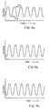
source, the read back signal from the recorded marks is shown in FIG. 4a with
readout signal varied between Vmc corresponding to the reflectivity of the mixed
crystalline phase, and Vma corresponding to the reflectivity of the mixed
amorphous phase. Vmc is higher than Vsub corresponding to the reflectivity of the
unrecorded element with sub-layers 3a and 3b.
As discussed earlier, regions with Vma were those exposed to Pw,
melted and quenched into the amorphous state of the mixed composition. The
regions with Vmc, on the other hand, were exposed to Pe. These regions were also
melted and mixed, but they crystallized after the laser exposure because of the
slower cooling rate.
Onto the same data track, a 10T data pattern was then overwritten
using the same write strategy. The readout signal is shown in FIG. 4b. Again the
signal varies between Vmc and Vma and the readout waveform is very similar to
that observed after the first write. FIG. 4c shows the readout waveform after 10
direct overwrites. Essentially no change is observed between the three
waveforms.
These results demonstrated that a disk according to the present
invention show stable recording performance right from the first recording
without any need for initializing or blending process steps.
COMPARATIVE EXAMPLE 1
On the same disk used in Example 1 above, another recording
experiment was performed. In this experiment all parameters were identical to
those used in Example 1 except the level of Pe was lowered to 5 mW. The
selection of this power level was to mimic the conventional recording processes.
In conventional recording processes Pe only heats the recording material to an
elevated temperature to accelerate the crystallization process, but it does not heat
the material to above the melting point.
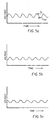
The readout waveform after the first recording is shown in FIG. 4d.
Now the readout level varies only between Vma and Vsub. Those regions with Vma
were again exposed to Pw, melted, mixed, and quenched into the amorphous
phase of the mixed composition. The region with Vsub, on the other hand, were
those exposed to Pe. Because of the lower power level used for Pe, these regions
were essentially unchanged by the laser exposure and remained as sub-layers 3a
and 3b retaining the original reflectivity.
Using the same parameters, a 10T pattern was overwritten on the
same data track. The readout waveform now looked like that in FIG. 4e. The
bottom level of the waveform was uniform at Vma but the top reflectivity level
varied from peak to peak. This is explained as follows. The low Pe used was not
sufficient to cause melting of the material. For regions exposed to Pe in the first-write,
the second exposure to Pe caused no change in the material and the
reflectivity stayed at Rsub. For regions exposed to Pw in the first write, and turned
into the amorphous phase of the mixed composition, the exposure to Pe caused
them to crystallize. These regions attained Vmc. Due to the two different data
patterns used for the two writes, there was a gradation in the degree of overlaps
between the two laser trains, causing varying length steps in reflectivity, as
illustrated in FIG. 3c, within the regions exposed to Pe on the second write.
Because of the small feature size involved, however, these steps could not be
resolved by the read-back laser light. Instead, the varying lengths of the steps
were manifested as different reflectivity levels. This variability in the top readout
level can cause readout errors and therefore is not desirable.
After several overwrites all of the materials on the data track would
have been melted at least once and turned into the mixed composition. The state
of the material was now determined only by the last laser exposure: exposure to
Pw yielded Vma and exposure to Pe yielded Vmc. FIG. 4f shows the readout
waveform after ten direct-overwrites. A uniform waveform was indeed observed,
with peak and bottom readout levels at Vmc and Vma, respectively.
This example illustrates the deficiency of the conventional
recording method. When low Pe level is used, only the region exposed to Pw is
melted and mixed. It takes several write cycles to cause the entire data track to
mix. The use of the high Pe is advantageous not only for the rewriteable phase-change
optical recording element of the present invention. Even for conventional,
single layer rewriteable phase-change optical recording element melting is
frequently needed for the phase-change material to reach the stable phase for
cycling. For AgInSbTe material, for example, it has been suggested that the
optimum recording is only achieved after the recording material is segregated into
a dispersion of AgInTe2 in the Sb crystalline phase through melting.
COMPARATIVE EXAMPLE 2
Another disk sample was fabricated as in Example 1, except the
thickness of the Sb sub-layer 3a was reduced to 7.4 nm and the thickness of the
TeIn0.37 sub-layer 3b was increased to 8.5 nm. This change in the relative
thickness of the two sub-layers 3a and 3b kept the optical and thermal packages of
the recording disk essentially unchanged, but caused a significant change in the
composition of the recording layer 3 after mixing. The composition of the mixed
material now became Sb0.511Te0.357In0.132. The higher Te concentration resulted in
a much slower crystallization rate after melting than the composition used in
Example 1. The reflectivity of the disk before and after the 16 hours room
temperature keeping was similar to that observed for the disk in Example 1.
The same recording experiment was carried out using a write
strategy as illustrated in FIG. 2a with the parameters: Pw = 11 mW, Pe = 7.0 mW,
Pb = 1 mW, T1 = 0.32T, T2 = 0.32 T and T3 = 0.8 T. Using an 11T tone as the
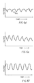
signal source, the read back signal from the recorded marks is shown in FIG. 5a
with levels varied between Vma and a value Vx that is lower than Vsub but higher
than Vma. These results can be understood as follows. As discussed earlier,
regions with Vma were those exposed to Pw, melted and quenched into the
amorphous state of the mixed composition. The regions with the new level, Vx,
on the other hand, were exposed to Pe. These regions were also melted and mixed
and, contrary to that observed in Example 1, in this case the phase-change
material, because of the slower crystallization rate, also amorphized. Because of
the slower cooling rate, the amorphized region was smaller than that achieved
after the exposure to Pw, giving rise the read back level Vx that was higher than
Vma.
Onto the same data track, a 10T data pattern was then overwritten
using the same write strategy. The readout signal is shown in FIG. 5b. Again the
readout varied between Vx and Vma and the readout waveform was very similar to
that observed after the first write. FIG. 5c shows the readout waveform after 10
direct overwrites. The qualitative features are very similar in the three
waveforms.
This example illustrates that if the crystallization speed of the
phase-change material is low, high Pe cannot be used to achieve good recording
performance.
COMPARATIVE EXAMPLE 3
A low Pe recording experiment was performed on the disk used in
Comparative Example 2. All parameters were identical to those used in that
example except the value of Pe was reduced to 5.0 mW.
The readout waveforms after the first write, after the first overwrite
with a 10T data pattern, and after 10 direct overwrites are shown in FIG. 5d, FIG.
5e, and FIG. 5f, respectively. These waveforms are very similar to the
corresponding waveforms in FIG. 4, and their results are similarly interpreted.
Thus, if a relatively slow-crystallizing material is used with low Pe,
the recording behavior is "normal" after the melting and mixing have been
completed. In this Comparative Example 3 the melting and mixing were
accomplished by repeating the overwrite a few times. It is also possible to
perform the function through a blending process using a separate step during the
disk manufacturing process. In this process a laser light with enough power to
melt and mix the material is scanned over the disk surface as suggested by
Japanese Patent Application JP A10-226173. In fact the readout level would
decrease from Vsub to Vx as a result since the material is not fast enough to
crystallize after melting by the scanning laser, just as it is not fast enough to
crystallize after melting by Pe.
COMPARATIVE EXAMPLE 4
Another disk sample was fabricated as in Example 1, except the
thickness of the Sb sub-layer 3a was increased to 9.4 nm and the thickness of the
TeIn037 sub-layer 3b was reduced to 6.0 nm. This change in the relative thickness
of the two sub-layers 3a and 3b kept the optical and thermal packages of the
recording disk similar to the other disks, but resulted in a significant change in the
composition of the recording layer after mixing. The composition of the mixed
material now became Sb0..652Te0.254In0.094. The lower Te concentration resulted in
a much faster crystallization rate after melting than the composition used in
Example 1. The reflectivity of the disk before and after the 16 hours room
temperature keeping was similar to that observed for the disk in Example 1.
The same recording experiment was done using a write strategy as
illustrated in FIG. 2a with the parameters: Pw = 11 mW, Pe = 7.0 mW, Pb = 1
mW, T1 = 0.32T, T2 = 0.32 T and T3 = 0.8 T. Using an 11T tone as the signal
source, the read back signal from the recorded marks is shown in FIG. 6a with
levels varied between Vmc and a value Vy that was lower than Vsub but higher than
Vma. These results can be understood as follows. Regions with Vy were those
exposed to Pw, melted and quenched into the amorphous state of the mixed
composition. Because of the faster crystallization rate of the phase-change
material used in this case, however, the quenching rate was not quite enough and
much of the molten area was recrystallized upon solidification. This resulted in
smaller amorphous spots with a read-back value Vy that is higher than Vma. The
regions exposed to Pe, on the other hand were melted and recrystallized as in
Comparative Example 1. These regions achieved the readout value Vmc.
Onto the same data track, a 10T data pattern was then overwritten
using the same write strategy. The readout signal is shown in FIG. 6b and that
after 10 direct overwrites is shown in FIG. 6c. In both cases the qualitative
features were very similar to that in FIG. 6a. The small decrease in Vy with
cycling is believed to be due to a change in crystallization rate of this material
with cycling.
This example illustrates that if the crystallization speed of the
phase-change material is too high, optimum performance cannot be achieved even
with high Pe.
COMPARATIVE EXAMPLE 5
A low Pe recording experiment was performed on the disk used in
Comparative Example 4. All parameters were identical to those used in that
example except the value of Pe was reduced to 5.0 mW.
The readout waveforms after the first write, after the first overwrite
with a 10T data pattern, and after 10 direct overwrites are shown in FIG. 6d, FIG.
6e, and FIG. 6f, respectively. These waveforms were very similar to the
corresponding waveforms in FIG. 4 except that the signal level corresponding to
the amorphous state was somewhat higher than that in FIG. 4 indicating that the
amorphous phase was not fully quenched due to the high crystallization rate.
Thus, if an overly fast crystallizing material is used with low Pe, it still takes
several overwrite cycles before full mixing can be achieved. Even after full
mixing the recording performance is inferior due to difficulty in achieving full
amorphization.
Example 2:
The above examples demonstrated the importance of selecting
phase-change materials with appropriate crystallization rate. In all phase-change
alloys, the crystallization rate is strongly dependent on alloy composition. To
determine the optimum composition range in the SbTeIn alloy system, a series of
disk samples were made as in Example 1. In each disk the recording layer 3
includes two sublayers 3a and 3b. The first sub-layer 3a is Sb and the second sub-layer
3b has a composition expressed by TeInm. These sub-layers 3a and 3b were
prepared by sputtering from an Sb target and a TeInm target respectively. When
combined, the composition of the recording layer 3 is represented by the formula
Sb1-x-mxTexInmx. The value of x can be varied by changing the relative thickness
of the sub-layers 3a and 3b, and the value of m can be varied by using different
TeInm targets. For this example, the total thickness of the sub-layers 3a and 3b
was kept at about 16 nm.
These disks were tested using the Pulstec tester as described
earlier. A random EFM data pattern was recorded on each disk using a write
strategy as illustrated in FIG. 2. Same parameters Pb = 0.5 mW, T1 = 0.32T, T2 =
0.32 T and T3 = 0.8 T were used for all disks but the value of Pw and Pe was
optimized for each individual disks. The readout data-to-clock jitter of the
recorded data in nano-seconds was used as an indication for the disk quality. Low
jitter values indicate good recording performance. Because these disks were
rewriteable disks, we measured the jitter values after 10 direct overwrite cycles.
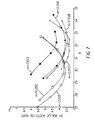
These values are plotted in FIG. 7 below, wherein each curve represents a distinct
m value and each point on the curves represents a disk with a distinct x value.
It has been found that disk performance depends strongly on both x
and m. If m is less than 0.2, the recorded data are not stable. Heating the disk at
80°C for 16 hours caused the recorded data to disappear. If m is larger than 0.65,
we could not obtain good recording performance at any x value. For m values
between these two extremes, the disk performance is a strong function of x.
Although the preferred range of x depends on m, FIG. 7 shows that good
recording performance can be achieved within the range 0.28 < x < 0.35.