EP1128463A2 - Reception circuit and adaptive array antenna system - Google Patents
Reception circuit and adaptive array antenna system Download PDFInfo
- Publication number
- EP1128463A2 EP1128463A2 EP01104043A EP01104043A EP1128463A2 EP 1128463 A2 EP1128463 A2 EP 1128463A2 EP 01104043 A EP01104043 A EP 01104043A EP 01104043 A EP01104043 A EP 01104043A EP 1128463 A2 EP1128463 A2 EP 1128463A2
- Authority
- EP
- European Patent Office
- Prior art keywords
- phase
- reception
- signal
- circuit
- section
- Prior art date
- Legal status (The legal status is an assumption and is not a legal conclusion. Google has not performed a legal analysis and makes no representation as to the accuracy of the status listed.)
- Withdrawn
Links
Images



Classifications
-
- H—ELECTRICITY
- H01—ELECTRIC ELEMENTS
- H01Q—ANTENNAS, i.e. RADIO AERIALS
- H01Q3/00—Arrangements for changing or varying the orientation or the shape of the directional pattern of the waves radiated from an antenna or antenna system
- H01Q3/26—Arrangements for changing or varying the orientation or the shape of the directional pattern of the waves radiated from an antenna or antenna system varying the relative phase or relative amplitude of energisation between two or more active radiating elements; varying the distribution of energy across a radiating aperture
-
- H—ELECTRICITY
- H01—ELECTRIC ELEMENTS
- H01Q—ANTENNAS, i.e. RADIO AERIALS
- H01Q3/00—Arrangements for changing or varying the orientation or the shape of the directional pattern of the waves radiated from an antenna or antenna system
- H01Q3/26—Arrangements for changing or varying the orientation or the shape of the directional pattern of the waves radiated from an antenna or antenna system varying the relative phase or relative amplitude of energisation between two or more active radiating elements; varying the distribution of energy across a radiating aperture
- H01Q3/267—Phased-array testing or checking devices
-
- H—ELECTRICITY
- H01—ELECTRIC ELEMENTS
- H01Q—ANTENNAS, i.e. RADIO AERIALS
- H01Q3/00—Arrangements for changing or varying the orientation or the shape of the directional pattern of the waves radiated from an antenna or antenna system
- H01Q3/26—Arrangements for changing or varying the orientation or the shape of the directional pattern of the waves radiated from an antenna or antenna system varying the relative phase or relative amplitude of energisation between two or more active radiating elements; varying the distribution of energy across a radiating aperture
- H01Q3/2605—Array of radiating elements provided with a feedback control over the element weights, e.g. adaptive arrays
-
- H—ELECTRICITY
- H01—ELECTRIC ELEMENTS
- H01Q—ANTENNAS, i.e. RADIO AERIALS
- H01Q3/00—Arrangements for changing or varying the orientation or the shape of the directional pattern of the waves radiated from an antenna or antenna system
- H01Q3/26—Arrangements for changing or varying the orientation or the shape of the directional pattern of the waves radiated from an antenna or antenna system varying the relative phase or relative amplitude of energisation between two or more active radiating elements; varying the distribution of energy across a radiating aperture
- H01Q3/30—Arrangements for changing or varying the orientation or the shape of the directional pattern of the waves radiated from an antenna or antenna system varying the relative phase or relative amplitude of energisation between two or more active radiating elements; varying the distribution of energy across a radiating aperture varying the relative phase between the radiating elements of an array
-
- H—ELECTRICITY
- H01—ELECTRIC ELEMENTS
- H01Q—ANTENNAS, i.e. RADIO AERIALS
- H01Q3/00—Arrangements for changing or varying the orientation or the shape of the directional pattern of the waves radiated from an antenna or antenna system
- H01Q3/26—Arrangements for changing or varying the orientation or the shape of the directional pattern of the waves radiated from an antenna or antenna system varying the relative phase or relative amplitude of energisation between two or more active radiating elements; varying the distribution of energy across a radiating aperture
- H01Q3/30—Arrangements for changing or varying the orientation or the shape of the directional pattern of the waves radiated from an antenna or antenna system varying the relative phase or relative amplitude of energisation between two or more active radiating elements; varying the distribution of energy across a radiating aperture varying the relative phase between the radiating elements of an array
- H01Q3/34—Arrangements for changing or varying the orientation or the shape of the directional pattern of the waves radiated from an antenna or antenna system varying the relative phase or relative amplitude of energisation between two or more active radiating elements; varying the distribution of energy across a radiating aperture varying the relative phase between the radiating elements of an array by electrical means
- H01Q3/42—Arrangements for changing or varying the orientation or the shape of the directional pattern of the waves radiated from an antenna or antenna system varying the relative phase or relative amplitude of energisation between two or more active radiating elements; varying the distribution of energy across a radiating aperture varying the relative phase between the radiating elements of an array by electrical means using frequency-mixing
Definitions
- the present invention relates to a reception circuit and an adaptive array antenna system using the same and, more particularly, to a reception circuit and adaptive array antenna system which can accurately control a propagation delay phase difference at a reception section for a reception signal.
- an adaptive array antenna As a receiver antenna, an adaptive array antenna is available, whose beam can be electronically directed in the arriving direction of radio waves, i.e., whose directivity can be adjusted.
- This adaptive array antenna is widely used as an antenna suited to mobile reception, and various types of adaptive array antennas have been proposed.
- an adaptive array antenna system has a plurality of antenna elements and is designed to obtain a desired reception signal by synthesizing outputs from reception circuits provided for the respective antenna elements.
- Each of the conventional reception circuits serving as preprocessing sections combined with the respective antenna elements of the above adaptive array antenna includes an oscillator for a local oscillation signal.
- the respective oscillators are not necessarily consistent with each other in terms of phase, and there are phase errors between local oscillation signals. For this reason, when frequency conversion is performed by a mixer in each radio signal reception section (to be referred to as a reception section), the corresponding phase error is added to the reception signal.
- each signal after addition varies in passing phase at the corresponding reception circuit. That is, this phase is not fixed. It is therefore impossible to detect a propagation delay phase difference upon reception by the antenna at the subsequent stage.
- a propagation delay phase difference in each reception circuit is not controlled. For this reason, in an adaptive array antenna or the like designed to operate by using a plurality of reception circuits at once, in particular, a random propagation delay phase different in each reception circuit directly influences the performance of the apparatus in use. That is, when reception circuits are used for an adaptive array antenna system or the like, since a propagation delay phase difference of a reception signal cannot be accurately calculated, correction and the like cannot be performed. If, therefore, a propagation delay amount in each reception circuit can be managed and controlled, the apparatus performance can be improved.
- a shared synthesizer scheme may be provided.
- an example of this arrangement is disclosed in Japanese Patent Laid-Open No. 10-224138.
- oscillators equal in number to channels must be prepared.
- signals since signals must be distributed to the respective reception circuits through a coaxial cable or the like, the apparatus becomes bulky.
- a reception circuit comprising a reception section for performing frequency conversion of an input signal by using a local frequency signal generated by phase comparing operation, and a control section for removing a passing phase error, added in the reception section, on the basis of a phase comparison signal output from the reception section.
- Fig. 1A shows a reception circuit used for the adaptive array antenna system of the present invention shown in Fig. 1B.
- a reception circuit 100 includes an antenna 10-1, a reception section 11-1 for outputting a signal IF-1 obtained by converting an RF signal received through the antenna 10-1 into a signal having a lower frequency and a phase comparison signal fr-1, a control section 12 for removing a passing phase error from the signal IF-1 on the basis of the phase comparison signal fr-1, and a reference oscillator 13 for generating a high-precision reference signal and outputting it to the control section 12.
- the signal received by the antenna 10-1 is input to the reception section 11-1 to be subjected to frequency conversion (down-conversion) and analog/digital conversion.
- the resultant signal IF-1 is output to the control section 12.
- An output from the reference oscillator 13 is input to the reception section 11-1 to be used for phase comparison in a circuit (PLL circuit to be described later) for generating a local oscillation signal for down-conversion.
- the phase comparison signal fr-1 obtained in the process of generating'the local oscillation signal is output from the reception section 11-1 to the control section 12.
- Fig. 1B shows the adaptive array antenna system according to the first embodiment of the present invention.
- the adaptive array antenna system shown in Fig. 1B is made up of a plurality of reception circuits 100, each shown in Fig. 1A.
- An adaptive array antenna system 200 in Fig. 1B will be described in detail below, together with the operation of the reception circuit 100 in Fig. 1A.
- the adaptive array antenna system 200 is made up of n reception circuits 100.
- the system 200 includes n antennas 10-1 to 10-n in correspondence with the reception circuits 100. All the antennas 10-1 to 10-n are omnidirectional and arranged at intervals of ⁇ /4 ( ⁇ is the wavelength of a frequency in use) or more.
- the respective reception circuits 100 share the control section 12 and reference oscillator 13.
- reception circuit 100 in Fig. 1A is configured to correspond to one block in the adaptive array antenna system 200.
- Fig. 2 shows the superheterodyne reception section 11-n.
- the reception sections 11-1 to 11-n have the same arrangement.
- the reception section 11-n is comprised of an amplifier 21 which has low-NF (Noise Factor) characteristics and amplifies a signal received by the antenna 10-n, a mixer 22 which is formed by a double-balanced mixer, transistor mixer, or the like and down-converts an output signal from the amplifier 21 on the basis of a PLL (Phase Locked Loop) output, a PLL circuit 25 for supplying a PLL output to the mixer 22, a filter 23 which is constituted by a SAW (Surface Acoustic Wave) element and the like and receives an output from the mixer 22 to remove out-of-band signals from the output, and an A/D converter 24 for converting the analog signal output from the filter 23 into the signal IF-n and outputting it to the control section 12.
- NF Noise Factor
- a reference signal from the reference oscillator 13 is input to the PLL circuit 25.
- the PLL circuit 25 outputs the phase comparison signal fr-n to the control section 12.
- Fig. 3 shows the PLL circuit 25.
- the PLL circuit 25 generates a local oscillation signal f used for down-conversion by the mixer 22 on the basis of an output signal fref from the reference oscillator 13 (Fig. 1B).
- the PLL circuit 25 is comprised of an oscillator 30 formed by a VCO (Voltage-Controlled Oscillator) or the like, a frequency divider 31 for frequency-dividing an output from the oscillator 30, a reference frequency divider 32 for frequency-dividing the signal fref from the reference oscillator 13 (Fig. 1B), a phase comparator 33 for comparing the phase of an output signal fp (Fig. 4B) from the frequency divider 31 with that of an output signal f'ref (Fig.
- VCO Voltage-Controlled Oscillator
- phase comparison signal fr (Fig. 4C) output from the charge pump 34 is output to the oscillator 30 and control section 12 (Fig. 1B).
- Fig. 5 shows the control section 12.
- the control section 12 includes n phase correction sections 40-1 to 40-n corresponding to the reception sections 11-1 to 11-n.
- the phase correction sections 40-1 to 40-n respectively have phase shifters 41-1 to 41-n. That is, the control section 12 includes the n phase correction sections 40-1 to 40-n corresponding to the n antennas 10-1 to 10-n.
- the phase correction sections 40-1 to 40-n respectively incorporate the phase shifters 41-1 to 41-n for removing phase errors from the signals IF-1 to IF-n by using the phase comparison signals fr-1 to fr-n output from the reception circuit 11.
- the processing performed by the control section 12 is processing based on digital signals, and hence can be implemented by either software or software.
- the reception signals received through the antennas 10-1 to 10-n are frequency-converted in the reception sections 11-1 to 11-n and output as the signals IF-1 to IF-n to the control section 12.
- the reception sections 11-1 to 11-n perform phase comparison by using the PLL circuits 25 in the process of generating the local oscillation signals f for frequency conversion and output the resultant phase comparison signals fr-1 to fr-n to the control section 12.
- the control section 12 removes the phase errors added to the signals IF-1 to IF-n in the reception sections 11-1 to 11-n by using the phase comparison signals fr-1 to fr-n, and fixes (synchronizes) passing phases between the respective reception sections 11. With this process, a phase deviation between the respective demodulated signals represents a reception delay phase to the antenna. This stabilizes the operation of the adaptive array antenna system and improves the reliability. Note that this phase detection is unique to the adaptive array antenna system and not directly relevant to the present invention. Therefore, a detailed description of this operation will be omitted.
- reception sections 11-1 to 11-n will be further described in detail next with reference to Fig. 2. Although the operation of the reception section 11-n will be described as an example, the same applies to the remaining reception sections.
- the reception signal input to the reception section 11-n through the antenna 10-n is amplified by the low-NF amplifier 21.
- the amplified signal is frequency-converted (down-converted) by the mixer 22 using the local oscillation signal f from the PLL circuit 25.
- the filter 23 removes unnecessary radiation outside the pass band from the output from the mixer 22 and passes only a signal having a desired frequency.
- the signal (analog signal) passing through the filter 23 is converted into the digital signal IF-n by the A/D converter 24. This signal is then output to the control section 12.
- the local oscillation signal f is generated by the PLL circuit 25 using the reference signal fref from the reference oscillator 13.
- a phase comparison signal used for phase comparison is output as the signal fr-n to the control section 12.
- the output signal fref from the reference oscillator 13 is input to the reference frequency divider 32 to be frequency-divided into the predetermined frequency f'ref.
- the frequency divider 31 frequency-divides an output from the oscillator (VCO) 30 into a signal having the same frequency as that of the output f'ref from the reference frequency divider 32.
- the phase comparator 33 compares the phase of the output fp from the frequency divider 31 with that of the output f'ref from the reference frequency divider 32 and outputs the resultant signal as a digital signal representing the phase difference between the two signals.
- This digital signal is input to the charge pump 34 and output to the oscillator 30.
- the oscillation frequency of the oscillator 30 changes accordingly, thereby obtaining a desired frequency.
- the local oscillation signal f from the oscillator 30 is output to the mixer 22.
- the signal f'ref shown in Fig. 4A is output from the highly stable reference oscillator 13, and hence has a constant clock.
- the signal fp is output from the oscillator 30 formed by a VCO, and hence changes in oscillation frequency in accordance with the voltage applied from the charge pump 34.
- the phase comparator 33 compares the phase of this signal f'ref with that of the signal fp to make them have the same frequency.
- the control section 12 detects only the propagation delay phase at the time of reception through the antenna by subtracting the phase errors of local oscillation signals added in the reception sections 11-1 to 11-n.
- the signals IF-1 to IF-n and signals fr-1 to fr-n are input in pairs to the corresponding phase shifters 41-1 to 41-n.
- the phase shifters 41-1 to 41-n lead the phases of the signals IF-1 to IF-n.
- phase shifter 41 leads the phase.
- the propagation delay phase differences received by the antennas 10-1 to 10-n can be directly detected from the phase shifter outputs.
- the signals fr-1 to fr-n must be synchronized with the signals IF-1 to IF-n. For this reason, synchronization is achieved by starting phase correction of the signals IF-1 to IF-n with reference to the timing at which the oscillation frequency of the local oscillation signal f generated by the PLL circuit 25 is locked. With this operation, when the phase of the local oscillation signal f advances, the phase can be delayed by the phase shifter, and vice versa.
- the phase comparison signals fr-1 to fr-n that have already been used in the process of generating the local oscillation signal f in the reception circuit 100 are used to correct passing phase differences in the reception circuit 100, and the phase added to the local oscillation signal f in the reception circuit 100 is removed. Then, the passing phases between the signals received through the antennas 10-1 to 10-n and the demodulated outputs are fixed. This greatly contributes to an improvement in the performance of an adaptive array antenna system or the like when the present invention is applied thereto.
- FIG. 6 shows the reception section in the second embodiment.
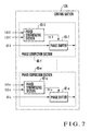
- Fig. 7 shows a control section 12A suited to this reception section. Note that since the overall system configuration of the second embodiment is the same as that of the first embodiment, a description thereof will be omitted.
- a reception section 11'-n performs down-conversion in two steps by using two PLL circuits 65 and 66. Consequently, two mixers 60 and 62 for down-conversion and two filters 61 and 63 for removing unnecessary radiation are used.
- Phase comparison signals fr1-n and fr2-n from the PLL circuits 65 and 66 are generated in the same manner as the signal fr in Fig. 4C.
- a control section 12 performs phase correction by using these signals.
- Reference numeral 64 denotes an A/D converter.
- the control section 12A further includes n phase synthesizing sections 42-1 to 42-n in correspondence with phase shifters 41-1 to 41-n. That is, the phase correction sections 40-1 to 40-n forming the control section 12A are constituted by the phase shifters 41-1 to 41-n and phase synthesizing sections 42-1 to 42-n.
- the phase shifter 41-1 receives a signal IF-1 from the reception section 11'-n, and the phase synthesizing section 42-1 as the counterpart receives phase comparison signals fr1-1 and fr2-1 from the reception section 11'-n.
- An output fr'-1 from the phase synthesizing section 42-1 is input to the phase shifter 41-1.
- phase comparison signals fr1-1 to fr1-n and fr2-1 to fr2-n are input in pairs to the corresponding the phase synthesizing sections 42-1 to 42-n.
- the phase synthesizing sections 42-1 to 42-n synthesize the phase of a local oscillation signal f1 with that of a local oscillation signal f2.
- the phase shifters 41-1 to 41-n perform phase correction by using synthetic signals fr'-1 to fr'-n from the phase synthesizing sections 42-1 to 42-n.
- phase comparison signal synthesizing operation in the phase synthesizing sections 42-1 to 42-n will be described with reference to Figs. 8A to 8C.
- the phase synthesizing section 42-n receives the phase comparison signals fr1-n and fr2-n shown in Figs. 8A and 8B.
- the phase synthesizing section 42-n outputs a signal fr'-n obtained by adding phase difference signals based on the phase comparison signals fr1-n and fr2-n on the time axis as shown in Fig. 8C.
- the signal fr1-n indicates a phase lag
- the signal fr2-n indicates an in-phase state. Therefore, the signal fr'-n (Fig. 8C) indicates only a phase lag portion of the signal fr1-n.
- the signal fr1-n indicates a phase lead
- the signal fr2-n indicates a phase lag.
- the pulse width of the signal fr2-n is larger than that of the signal fr1-n, the phase error indicated by the signal fr2-n is large.
- the pulse width of the signal fr'-n is therefore determined to delay the phase by the difference represented by (fr2-n) - (fr1-n).
- the phase shifters 41-1 to 41-n perform phase correction on the basis of the signal fr'-n including the phase information of the signals fr1-n and fr2-n.
- phase correction can be performed on the basis of a plurality of phase comparison signals, the phase differences between reception signals which are unique to the respective antennas can be corrected, i.e., normalized, to be fixed, thereby stably operating the adaptive array antenna system.
- each of the reception circuits constituting the adaptive array antenna system described above can be effectively used singly depending on the application purpose. More specifically, for example, this circuit can be used to remove, control, or fix the phase lag of a passing signal with respect to an input signal while performing frequency conversion.
- the reception circuit in this case is comprised of reception sections 11-1 and 11'-1 which receive RF signals and include PLL circuits, a reference oscillator 13 for supplying a reference frequency to the reception sections 11-1 and 11'-1, and control sections 12 and 12A which receive down-conversion outputs from the reception sections 11-1 and 11'-1 and phase comparison signals.
- the control sections 12 and 12A provide low-frequency signal outputs controlled to have predetermined phase relationships with input signals.
- phase errors between local oscillation signals which are added in the reception sections are removed on the basis of phase comparison signals in the process of generating the local oscillation signals, the phase between a reception signal and a demodulated signal in each reception circuit is fixed, contributing to stabilization of an apparatus using such reception circuits.
- phase correction is performed by removing the phase errors, added to reception circuit output signals, by using phase comparison signals in the process of generating the respective local oscillation signals, thereby correcting passing phases in the same manner as described above.
- phase correction is performed by only using the arrangement that effectively uses signals from existing constituent elements, i.e., phase comparison signals in the process of generating local oscillation signals, an unnecessary increase in apparatus size can be suppressed.
Landscapes
- Radio Transmission System (AREA)
- Variable-Direction Aerials And Aerial Arrays (AREA)
- Superheterodyne Receivers (AREA)
- Stabilization Of Oscillater, Synchronisation, Frequency Synthesizers (AREA)
Abstract
Description
Claims (13)
- A reception circuit characterized by comprising:a reception section (11-1, 11'-1) for performing frequency conversion of an input signal by using a local frequency signal (f, f1, f2) generated by phase comparing operation; anda control section (12, 12A) for removing a passing phase error, added in said reception section, on the basis of a phase comparison signal (fr-1, fr1-1, fr1-2) output from said reception section.
- A circuit according to claim 1, wherein said control section comprises a phase shifter (41-1) for shifting a phase of a reception output on the basis of the phase comparison signal from said reception section.
- A circuit according to claim 1, wherein
said reception section comprises:a first PLL (Phase Locked Loop) circuit (25, 65) for outputting a first phase comparison signal (fr-1, fr1-1) indicating a phase comparison by comparing a phase of an oscillation frequency of a first local oscillator (30) with a phase of an external reference frequency (fref), and for outputting a first local frequency signal (f, f1) by controlling the oscillation frequency of said local oscillator on the basis of the phase comparison result; anda first mixer circuit (22, 60) for down-converting an input signal by using the first local frequency signal from said first PLL circuit, andsaid control section fixes the passing phase of the reception output in said reception section by correcting the passing phase added in said reception section using at least the first phase comparison signal from said first PLL circuit. - A circuit according to claim 3, wherein
said reception section comprises:a second PLL circuit for outputting a second phase comparison signal (fr1-2) indicating a phase comparison by comparing a phase of an oscillation frequency of a second local oscillator with a phase of an external reference frequency (fref), and outputting a second local frequency signal (f2) by controlling the oscillation frequency of said second local oscillator on the basis of the phase comparison result; anda second mixer circuit (62) for down-converting an output from said first mixer by using the second local frequency signal from said second PLL circuit, andsaid control section fixes the passing phase of the reception output in said reception section by correcting the passing phase added in said reception section, using first and second phase comparison signals from said first and second PLL circuits. - A circuit according to claim 4, wherein
said control section comprises:a phase synthesizing section (42-1) for synthesizing the first and second phase comparison signals from said first and second PLL circuits; anda phase shifter (41-1) for shifting a phase of reception output on the basis of a synthetic phase comparison signal from said phase synthesizing section. - A circuit according to claim 3, further comprising a reference oscillator (13) for outputting an external reference frequency to said first PLL circuit.
- A circuit according to claim 1, wherein said control section removes a passing phase added in said reception section.
- An adaptive array antenna system characterized by comprising:a plurality of antennas (10-1 - 10-n);a reference oscillator (13) for outputting a reference frequency;a plurality of reception sections (11-1 - 11-n) which are provided in correspondence with said antennas, generate local frequency signals (f, f1, f2) by comparing a phase of the reference frequency from said reference oscillator with phases of local oscillation signals, and perform frequency conversion of input signals by using the generated local frequency signals; anda control section (12, 12A) for removing passing phase errors, added in said reception section, on the basis of phase comparison signals (fr-1, fr1-1, fr1-2) output from said reception sections.
- A system according to claim 8, wherein said control section comprises a phase shifter (41-1) for shifting a phase of a reception output on the basis of a phase comparison signal from said reception section.
- A system according to claim 8, wherein
said reception section comprises:a first PLL (Phase Locked Loop) circuit (25, 65) for outputting a first phase comparison signal (fr-1, fr1-1) indicating a phase comparison by comparing a phase of an oscillation frequency of said first local oscillator (30) with a phase of an external reference frequency (fref), and outputting a first local frequency signal (f, f1) by controlling the oscillation frequency of said local oscillator on the basis of the phase comparison result; anda first mixer circuit (22, 60) for down-converting an input signal by using the first local frequency signal from said first PLL circuit, andsaid control section fixes a passing phase of a reception output in said reception circuit by correcting a passing phase, added in said reception section, by using at least the first phase comparison signal from said first PLL circuit. - A system according to claim 10, wherein
said reception section comprises:a second PLL circuit for outputting a second phase comparison signal (fr1-2) indicating a phase comparison by comparing a phase of an oscillation frequency of said second local oscillator with the phase of the external reference frequency (fref), and outputting a second local frequency signal (f2) by controlling the oscillation frequency of said second local oscillator on the basis of the phase comparison result; anda second mixer circuit (62) for down-converting an output from said first mixer circuit by using the second local frequency signal from said second PLL circuit, andsaid control section fixes a passing phase of a reception output in said reception circuit by correcting a passing phase, added in said reception section, by using first and second phase comparison signals from said first and second PLL circuits. - A system according to claim 11, wherein
said control section comprises:a phase synthesizing section (42-1) for synthesizing the first and second phase comparison signals from said first and second PLL circuits; anda phase shifter (41-1) for shifting a phase of reception output on the basis of a synthetic phase comparison signal from said phase synthesizing section. - A circuit according to claim 8, wherein said control section removes a passing phase added in said reception section.
Applications Claiming Priority (2)
| Application Number | Priority Date | Filing Date | Title |
|---|---|---|---|
| JP2000042458 | 2000-02-21 | ||
| JP2000042458A JP3597101B2 (en) | 2000-02-21 | 2000-02-21 | Receiver circuit and adaptive array antenna system |
Publications (2)
| Publication Number | Publication Date |
|---|---|
| EP1128463A2 true EP1128463A2 (en) | 2001-08-29 |
| EP1128463A3 EP1128463A3 (en) | 2006-04-05 |
Family
ID=18565534
Family Applications (1)
| Application Number | Title | Priority Date | Filing Date |
|---|---|---|---|
| EP01104043A Withdrawn EP1128463A3 (en) | 2000-02-21 | 2001-02-20 | Reception circuit and adaptive array antenna system |
Country Status (6)
| Country | Link |
|---|---|
| US (1) | US6476765B2 (en) |
| EP (1) | EP1128463A3 (en) |
| JP (1) | JP3597101B2 (en) |
| KR (1) | KR20010083212A (en) |
| CN (1) | CN1312598A (en) |
| BR (1) | BR0101980A (en) |
Cited By (1)
| Publication number | Priority date | Publication date | Assignee | Title |
|---|---|---|---|---|
| WO2002089252A1 (en) * | 2001-04-26 | 2002-11-07 | Koninklijke Philips Electronics N.V. | A method and system for forming an antenna pattern |
Families Citing this family (9)
| Publication number | Priority date | Publication date | Assignee | Title |
|---|---|---|---|---|
| JP4183592B2 (en) * | 2003-09-26 | 2008-11-19 | 三洋電機株式会社 | Receiving method and apparatus |
| KR100706229B1 (en) * | 2004-12-21 | 2007-04-11 | 삼성전자주식회사 | Multiple transceiver system and method for compensating carrier frequency difference between embedded transceivers |
| RU2367068C1 (en) * | 2005-06-09 | 2009-09-10 | Макдоналд, Деттвилер Энд Ассошиэйтс Лтд. | Simplified system with active phased antenna array with spatial excitation |
| KR100784556B1 (en) * | 2005-11-23 | 2007-12-11 | 엘지전자 주식회사 | Dual feeding device of antenna using SPD switch |
| US7859459B2 (en) * | 2008-04-04 | 2010-12-28 | Panasonic Corporation | Phased array receivers and methods employing phase shifting downconverters |
| ES2654641T3 (en) * | 2009-07-01 | 2018-02-14 | Locata Corporation Pty Ltd | Method and apparatus for forming a beam |
| US9720875B2 (en) * | 2013-07-24 | 2017-08-01 | Silicon Laboratories Inc. | Receiver with signal arrival detection capability |
| KR101601068B1 (en) * | 2015-10-07 | 2016-03-08 | 서울대학교산학협력단 | Method, system and computer-readable recording medium for transmitting and receiving wideband signal by using phase array antenna |
| TWI773982B (en) * | 2019-05-22 | 2022-08-11 | 啟碁科技股份有限公司 | Beamforming device, calibration method and calibration system for the same |
Family Cites Families (13)
| Publication number | Priority date | Publication date | Assignee | Title |
|---|---|---|---|---|
| US3140490A (en) * | 1961-11-30 | 1964-07-07 | Sichak Associates | Communication system with automatic antenna beam steering |
| GB2056781B (en) * | 1979-08-10 | 1983-08-24 | Marconi Co Ltd | Antenna arrangements |
| US4367542A (en) * | 1981-03-23 | 1983-01-04 | Phillips Petroleum Company | Phase shifting of waveforms |
| US4879757A (en) * | 1987-05-07 | 1989-11-07 | Hazeltine Corp. | Tweet elimination, or reduction, in superheterodyne receivers |
| JP2559005B2 (en) * | 1993-01-07 | 1996-11-27 | 松下電器産業株式会社 | Double super tuner |
| JPH07245633A (en) * | 1994-03-04 | 1995-09-19 | Toshiba Corp | Digital data receiver |
| JP3450146B2 (en) | 1997-02-04 | 2003-09-22 | 三菱電機株式会社 | Directivity control circuit of adaptive array antenna |
| JP4015750B2 (en) * | 1998-05-14 | 2007-11-28 | 株式会社東芝 | Active array antenna system |
| KR100381812B1 (en) * | 1998-11-19 | 2003-04-30 | 니폰 덴신 덴와 가부시끼가이샤 | Adaptive array antenna device |
| JP3568839B2 (en) * | 1999-07-12 | 2004-09-22 | 株式会社国際電気通信基礎技術研究所 | Array antenna control device and control method |
| EP1777838B1 (en) * | 1999-12-15 | 2010-02-24 | Nippon Telegraph and Telephone Corporation | Adaptive array antenna transceiver apparatus |
| JP3851478B2 (en) * | 1999-12-16 | 2006-11-29 | 日本電信電話株式会社 | Adaptive array antenna device |
| JP3638108B2 (en) * | 2000-01-19 | 2005-04-13 | 三菱電機株式会社 | Antenna measuring apparatus and antenna measuring method |
-
2000
- 2000-02-21 JP JP2000042458A patent/JP3597101B2/en not_active Expired - Fee Related
-
2001
- 2001-02-19 BR BR0101980-5A patent/BR0101980A/en not_active IP Right Cessation
- 2001-02-20 EP EP01104043A patent/EP1128463A3/en not_active Withdrawn
- 2001-02-20 US US09/785,533 patent/US6476765B2/en not_active Expired - Fee Related
- 2001-02-21 KR KR1020010008605A patent/KR20010083212A/en not_active Ceased
- 2001-02-21 CN CN01104078A patent/CN1312598A/en active Pending
Cited By (1)
| Publication number | Priority date | Publication date | Assignee | Title |
|---|---|---|---|---|
| WO2002089252A1 (en) * | 2001-04-26 | 2002-11-07 | Koninklijke Philips Electronics N.V. | A method and system for forming an antenna pattern |
Also Published As
| Publication number | Publication date |
|---|---|
| US6476765B2 (en) | 2002-11-05 |
| KR20010083212A (en) | 2001-08-31 |
| JP3597101B2 (en) | 2004-12-02 |
| JP2001237631A (en) | 2001-08-31 |
| US20010050632A1 (en) | 2001-12-13 |
| BR0101980A (en) | 2001-12-04 |
| EP1128463A3 (en) | 2006-04-05 |
| CN1312598A (en) | 2001-09-12 |
Similar Documents
| Publication | Publication Date | Title |
|---|---|---|
| EP1914834B1 (en) | Monopulse radar apparatus | |
| WO2001029980A9 (en) | Multi-mode communications system with efficient oscillator synchronization | |
| US7054397B1 (en) | Mobile communication system having mobile stations and a base station | |
| US6476765B2 (en) | Reception circuit and adaptive array antenna system | |
| US6668025B1 (en) | Tuning demodulator for digitally modulated RF signals | |
| US8008979B2 (en) | Frequency synthesizer and radio transmitting apparatus | |
| US7778620B2 (en) | Controlling phase locked loop in a mobile station | |
| US20190260443A1 (en) | Phase Locked Loop, Phase Locked Loop Arrangement, Transmitter And Receiver And Method For Providing An Oscillator Signal | |
| US7688149B2 (en) | Phase locked loop, phase detecting method for the phase locked loop, and receiver using the same | |
| US6108389A (en) | Synchronization of internal coder-decoders of multiple microprocessors | |
| US20100119011A1 (en) | System and method for tuning fm synthesizer | |
| JP3342854B2 (en) | In-phase synthesis / phase difference detection circuit | |
| JP7652020B2 (en) | COMMUNICATION DEVICE, COMMUNICATION METHOD, AND PROGRAM | |
| JP3148320B2 (en) | Array antenna | |
| JP2002335178A (en) | Frequency scanning receiver | |
| JP2002325028A (en) | Frequency scanning receiver | |
| JP2004274474A (en) | DAB tuner and IC | |
| JP2851349B2 (en) | Array antenna in-phase synthesizer | |
| JP2000165279A (en) | Reception tracking correction circuit for fm receiving circuit | |
| JPH06188777A (en) | High frequency tuning receiver | |
| JPH07297757A (en) | Spread spectrum receiver | |
| JPH06104788A (en) | Superheterodyne receiver | |
| JPH08162834A (en) | Adaptive array antenna | |
| JPH1051341A (en) | Radio receiver circuit | |
| JP2001077616A (en) | In-phase synthesis / phase difference detection circuit |
Legal Events
| Date | Code | Title | Description |
|---|---|---|---|
| PUAI | Public reference made under article 153(3) epc to a published international application that has entered the european phase |
Free format text: ORIGINAL CODE: 0009012 |
|
| AK | Designated contracting states |
Kind code of ref document: A2 Designated state(s): AT BE CH CY DE DK ES FI FR GB GR IE IT LI LU MC NL PT SE TR |
|
| AX | Request for extension of the european patent |
Free format text: AL;LT;LV;MK;RO;SI |
|
| PUAL | Search report despatched |
Free format text: ORIGINAL CODE: 0009013 |
|
| AK | Designated contracting states |
Kind code of ref document: A3 Designated state(s): AT BE CH CY DE DK ES FI FR GB GR IE IT LI LU MC NL PT SE TR |
|
| AX | Request for extension of the european patent |
Extension state: AL LT LV MK RO SI |
|
| 17P | Request for examination filed |
Effective date: 20060224 |
|
| STAA | Information on the status of an ep patent application or granted ep patent |
Free format text: STATUS: THE APPLICATION HAS BEEN WITHDRAWN |
|
| 17Q | First examination report despatched |
Effective date: 20060622 |
|
| 18W | Application withdrawn |
Effective date: 20060614 |