EP1126305A2 - Electrostatic microshutter matrix having a high fill factor - Google Patents
Electrostatic microshutter matrix having a high fill factor Download PDFInfo
- Publication number
- EP1126305A2 EP1126305A2 EP01830085A EP01830085A EP1126305A2 EP 1126305 A2 EP1126305 A2 EP 1126305A2 EP 01830085 A EP01830085 A EP 01830085A EP 01830085 A EP01830085 A EP 01830085A EP 1126305 A2 EP1126305 A2 EP 1126305A2
- Authority
- EP
- European Patent Office
- Prior art keywords
- petal
- microshutter
- microshutters
- substrate
- matrix
- Prior art date
- Legal status (The legal status is an assumption and is not a legal conclusion. Google has not performed a legal analysis and makes no representation as to the accuracy of the status listed.)
- Granted
Links
Images
Classifications
-
- G—PHYSICS
- G02—OPTICS
- G02B—OPTICAL ELEMENTS, SYSTEMS OR APPARATUS
- G02B6/00—Light guides; Structural details of arrangements comprising light guides and other optical elements, e.g. couplings
- G02B6/24—Coupling light guides
- G02B6/26—Optical coupling means
- G02B6/35—Optical coupling means having switching means
- G02B6/351—Optical coupling means having switching means involving stationary waveguides with moving interposed optical elements
- G02B6/353—Optical coupling means having switching means involving stationary waveguides with moving interposed optical elements the optical element being a shutter, baffle, beam dump or opaque element
-
- G—PHYSICS
- G02—OPTICS
- G02B—OPTICAL ELEMENTS, SYSTEMS OR APPARATUS
- G02B6/00—Light guides; Structural details of arrangements comprising light guides and other optical elements, e.g. couplings
- G02B6/24—Coupling light guides
- G02B6/26—Optical coupling means
- G02B6/35—Optical coupling means having switching means
- G02B6/3564—Mechanical details of the actuation mechanism associated with the moving element or mounting mechanism details
- G02B6/3566—Mechanical details of the actuation mechanism associated with the moving element or mounting mechanism details involving bending a beam, e.g. with cantilever
-
- G—PHYSICS
- G02—OPTICS
- G02B—OPTICAL ELEMENTS, SYSTEMS OR APPARATUS
- G02B6/00—Light guides; Structural details of arrangements comprising light guides and other optical elements, e.g. couplings
- G02B6/24—Coupling light guides
- G02B6/26—Optical coupling means
- G02B6/35—Optical coupling means having switching means
- G02B6/3564—Mechanical details of the actuation mechanism associated with the moving element or mounting mechanism details
- G02B6/3568—Mechanical details of the actuation mechanism associated with the moving element or mounting mechanism details characterised by the actuating force
- G02B6/357—Electrostatic force
Definitions
- the present invention refers to electrostatically controlled microshutters.
- Electrostatic actuators suitable for use as actuators in microelectronic technology applications for operating mechanical devices and similar in conditions subject to vibration, such as in the automobile field for example, have already been produced in the past.
- These electrostatic actuators employ flexible, electrically conductive plates, also known as cilia, or petals, each with one end connected to a stator and the other end next to a motion translator.
- the application of voltage pulses between the petals and an electrode connected to the translator induces an electrostatic effect that causes the petals to adhere to the translator, resulting in latter moving with respect to the stator.
- An actuator of the above-indicated type is, for example, described in "Prospects of the Employment of Synchrotron Radiation in film electrostatic actuator technology" by V. L. Dyatloc, V.V. Konyaskin, B.S. Potopov and Yu. A. Pyankov, Nuclear Instruments and Methods in Physics Research, A359 (1995), pages 394-395.
- a microshutter of this type has, for example, been proposed in the Italian patent application TO98A001029 submitted by the same Applicant, still secret at the date of filing of this application.
- the previously proposed device includes a single, electrostatically controlled microshutter that includes:
- the object of this invention is that of realizing a matrix of electrostatically controlled microshutters of the above described type, in which the microshutters forming the matrix can be controlled individually or in groups and which exhibits a high fill factor, that is a high ratio between the area through which light can pass when each microshutter is open and the total area of the device.
- the object of the invention is a matrix of microshutters having a high fill factor, characterized in that it includes a number of microshutters arranged in a matrix, with one or more rows and one or more columns, in which each microshutter includes:
- the microshutters when they are all in their operative positions, they leave the spaces between the parallel rows of microshutters completely open to allow light to pass through, and so the entire area occupied by the matrix remains substantially transparent for the passage of light, except for the zones occupied by the substrates of the various rows that, since they are arranged in planes parallel to the direction in which the light rays pass, present a minimum section that blocks the light. No additional medium needs to pass through the part open to the light, other than that which is being propagated (air, vacuum, ).
- the thin plate forming the substrate of each microshutter can be made of silicon, glass, plastic or a metallic material. Using a single row of microshutters, the thickness of the substrate could be a few millimetres. In the case where it is desired to produce a microshutter matrix having a high fill factor, the thickness of the substrate must be much smaller, in the order of 20-40 microns for example.
- the layer of conductive material forming the electrode is applied on the substrate via evaporation, spin-coating, silkscreen printing or dipping and has a thickness of a few tens or hundreds of nanometres.
- the dielectric or ferroelectric insulation layer can have a thickness varying between 0.1 microns and a few tens of microns. This layer can also be obtained via silkscreen printing, vacuum deposition, spin-coating, dipping or, in the case of silicon, by oxidation.
- the thickness of the metal film forming the petal can range from a few fractions of a micron to several microns.
- the petal could also be composed of silicon or a metallized plastic material.
- the microshutter matrix can be electrically powered using means suitable for commanding the various microshutters individually. Partitioning can be effected both by electrically dividing the petals of a single line and by electrically dividing the electrodes associated with the various petals.
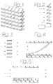
- number 1 indicates a matrix of microshutters 2 as a whole, these being arranged in a number of spaced-out rows, one above the other, with the supports 4 of the microshutters of each row parallel to the supports 4 of the microshutters 2 of the adjacent rows.
- the single microshutter 2 comprises a fixed support 4 including a substrate 5 in the form of a thin plate, a layer 6 acting as an electrode and an insulation layer 7.
- the substrate 5 is composed of silicon, or glass, or a metallic or plastic material.
- the preferable thickness of the substrate 5 is 20-40 microns. In implementations with just a single row of microshutters, this thickness could also be a few millimetres.
- a layer 6 of conductive material is applied on the substrate 5 via evaporation, spin-coating, silkscreen printing or dipping.
- the conductive layer is subsequently insulated with a dielectric or ferroelectric insulation layer, which can have a thickness varying between 0.1 microns and a few tens of microns.
- This layer can also be obtained via silkscreen printing, vacuum deposition, spin-coating, dipping or, in the case of silicon, by oxidation.
- the movable part is composed of a petal 8, in the form of a metallic film with a thickness ranging from a few fractions of a micron to several microns.
- the petal 8 could also be composed of silicon or a plastic material with a metallized layer.
- One end of the petal 8 is fixed to the surface of the fixed support 4.
- a metallic film 8 is used that, in its undeformed configuration, has a curved shape such that the film remains in the raised position illustrated in figures 2 and 4, namely away from the respective fixed support 4, until an electrical voltage is applied.
- the respective petals 8 have their free ends in contact with the substrates 5 of the overhead row of microshutters. In this state therefore, the light rays L cannot pass through the matrix 1.
- the device is equipped with means 9 for feeding an electrical voltage between each electrode 4 and the respective petal 8. The application of a voltage induces an electrostatic effect that causes the each petal 8 to adhere to its respective fixed support 4 (figure 3). In this state, the spaces between adjacent rows of microshutters are completely open for the passage of light rays L (figure 3).
- the matrix in accordance with the invention consequently exhibits a high ratio between the area that allows light to pass through and the total area of the matrix (fill factor).
- each microshutter returns to the rest state, illustrated in figure 4, under the inbuilt elasticity of the individual petals 8.
- the means of supplying electricity 9 can be arranged to individually feed the petal 8 and/or electrodes 6, thereby opening and closing the various microshutters 2 individually or in groups, and so realize all types of desired result.
- Microshutter matrices realized according to the above-described principles can be used to advantage in various applications of optical devices, such as optical scanning and display devices.
Landscapes
- Physics & Mathematics (AREA)
- General Physics & Mathematics (AREA)
- Optics & Photonics (AREA)
- Mechanical Light Control Or Optical Switches (AREA)
- Devices For Indicating Variable Information By Combining Individual Elements (AREA)
- Electrochromic Elements, Electrophoresis, Or Variable Reflection Or Absorption Elements (AREA)
Abstract
Description
- a fixed support, including
a substrate in the form of a thin plate,
an electrode composed of a thin film of electrically conductive material, applied to one side of the thin plate forming the substrate, and - a movable petal, composed of a thin film of electrically conductive and elastically deformable material, with only the part at one end rigidly connected to the said insulating film,
and in which the said microshutters are arranged in one or more spaced-out rows, one above the other, with the substrates of the microshutters of each row mutually coplanar and parallel with the substrates of the microshutters of the adjacent rows.
Claims (8)
- An electrostatic microshutter matrix having a high fill factor group, characterized in that it includes a number of electrostatically controlled microshutters (2), arranged in a matrix with one or more rows and one or more columns, in which each microshutter includes:a fixed support (4), includinga substrate (5) in the form of a thin plate,an electrode (6) composed of a thin film of electrically conductive material, applied to one side of the thin plate forming the substrate (5),a dielectric or ferroelectric insulating film (7)applied over the film forming the said electrode (6), anda movable petal (8), composed of a thin film of electrically conductive and elastically deformable material, with only the part at one end rigidly connected to the said insulation film (7),in which the said petal (8) has an undeformed rest state, where only the said part at one end of the petal (8) is in contact with the respective substrate (5), while the remainder of the petal (8) is curved so that that it is raised away from the substrate, and an operative, deformed position in which, due to the electrostatic effect following application of an electrical voltage between the said electrode (6) and the said petal (8), the petal (8) adheres completely to the said insulation film (7), the said petal ready to return to the said undeformed rest position under the effect of its intrinsic elasticity when the voltage between the said electrode (6) and said petal (8) is removed,in which the said microshutters (2) are arranged in one or more spaced-out rows, one above the other, with the substrates of the microshutters (2) of each row mutually coplanar and parallel with the substrates of the microshutters of the adjacent rows.
- A microshutter matrix according to claim 1, characterized in that the thin plate forming the substrate (5) is made of a material chosen from a metallic material, plastic material, glass or silicon.
- A microshutter matrix according to claim 1, characterized in that the said substrate (5) has a thickness ranging from a few microns to a few millimetres.
- A microshutter matrix according to claim 3, characterized in that the thickness of the said substrate (5) is between 20 and 40 microns.
- A microshutter matrix according to claim 1, characterized in that the said layer of conductive material forming the electrode (6) is realized via evaporation, spin-coating, silkscreen printing or dipping and has a thickness ranging between a few tens and a few hundreds of nanometres.
- A microshutter matrix according to claim 1, characterized in that the said insulation layer (7) is obtained via silkscreen printing, vacuum deposition, spin-coating, dipping or, in the case of silicon, by oxidation.
- A microshutter matrix according to claim 1, characterized in that each petal (8) is composed of an entirely metallic sheet, or a sheet of silicon or plastic material with an additional metallized layer.
- A microshutter matrix according to claim 1, characterized in that the means (9) of supplying an electrical voltage to the electrodes (6) and to the petals (8) of the various microshutters (2) in the matrix, are suitable for realizing the electrical partitioning of the petals (8) and/or the respective electrodes (6).
The whole is substantially as described and illustrated, and for the specified purposes.
Applications Claiming Priority (2)
| Application Number | Priority Date | Filing Date | Title |
|---|---|---|---|
| ITTO20000152 IT1319845B1 (en) | 2000-02-16 | 2000-02-16 | DIE OF ELECTROSTATIC MICRO-SHUTTERS WITH HIGH FILLING FACTOR. |
| ITTO200152 | 2000-02-17 |
Publications (3)
| Publication Number | Publication Date |
|---|---|
| EP1126305A2 true EP1126305A2 (en) | 2001-08-22 |
| EP1126305A3 EP1126305A3 (en) | 2002-01-23 |
| EP1126305B1 EP1126305B1 (en) | 2003-04-23 |
Family
ID=11457436
Family Applications (1)
| Application Number | Title | Priority Date | Filing Date |
|---|---|---|---|
| EP20010830085 Expired - Lifetime EP1126305B1 (en) | 2000-02-16 | 2001-02-09 | Electrostatic microshutter matrix having a high fill factor |
Country Status (4)
| Country | Link |
|---|---|
| EP (1) | EP1126305B1 (en) |
| DE (1) | DE60100197T2 (en) |
| ES (1) | ES2195986T3 (en) |
| IT (1) | IT1319845B1 (en) |
Cited By (1)
| Publication number | Priority date | Publication date | Assignee | Title |
|---|---|---|---|---|
| DE10215658A1 (en) * | 2002-04-09 | 2003-10-30 | Astrium Gmbh | Structure for optical masking has an array of masking elements each designed to assume translucent and non-translucent states along with a device to maintain the translucent state of the elements. |
Family Cites Families (3)
| Publication number | Priority date | Publication date | Assignee | Title |
|---|---|---|---|---|
| US3746785A (en) * | 1971-11-26 | 1973-07-17 | Bendix Corp | Deflectable membrane optical modulator |
| EP0246547A3 (en) * | 1986-05-22 | 1990-06-13 | Siemens Aktiengesellschaft | Optical image-processing arrangement |
| US5781331A (en) * | 1997-01-24 | 1998-07-14 | Roxburgh Ltd. | Optical microshutter array |
-
2000
- 2000-02-16 IT ITTO20000152 patent/IT1319845B1/en active
-
2001
- 2001-02-09 ES ES01830085T patent/ES2195986T3/en not_active Expired - Lifetime
- 2001-02-09 EP EP20010830085 patent/EP1126305B1/en not_active Expired - Lifetime
- 2001-02-09 DE DE2001600197 patent/DE60100197T2/en not_active Expired - Lifetime
Cited By (1)
| Publication number | Priority date | Publication date | Assignee | Title |
|---|---|---|---|---|
| DE10215658A1 (en) * | 2002-04-09 | 2003-10-30 | Astrium Gmbh | Structure for optical masking has an array of masking elements each designed to assume translucent and non-translucent states along with a device to maintain the translucent state of the elements. |
Also Published As
| Publication number | Publication date |
|---|---|
| DE60100197T2 (en) | 2004-05-19 |
| ES2195986T3 (en) | 2003-12-16 |
| IT1319845B1 (en) | 2003-11-03 |
| ITTO20000152A1 (en) | 2001-08-16 |
| EP1126305A3 (en) | 2002-01-23 |
| EP1126305B1 (en) | 2003-04-23 |
| DE60100197D1 (en) | 2003-05-28 |
Similar Documents
| Publication | Publication Date | Title |
|---|---|---|
| US4234245A (en) | Light control device using a bimorph element | |
| US7271945B2 (en) | Methods and apparatus for actuating displays | |
| US5239222A (en) | Electrostatic actuator using films | |
| KR100286486B1 (en) | Elastomeric Micro Electromechanical Systems | |
| CA2598740C (en) | Methods and apparatus for actuating displays | |
| EP1241507B1 (en) | An electrostatically-controlled optical micro-shutter with non-transparent fixed electrode | |
| KR101484646B1 (en) | Methods and apparatus for spatial light modulation | |
| EP1319969B1 (en) | Display material for electric paper and applications thereof | |
| KR960001941B1 (en) | Flat display device | |
| US12054384B2 (en) | MEMS comprising a movable structural element, and MEMS array | |
| AU2023225930B2 (en) | Piezo-electrophoretic film including patterned piezo polarities for creating images via electrophoretic media | |
| US7967456B2 (en) | Scalable size deformable pocket mirror with on-pocket bimorph actuator | |
| EP1126305B1 (en) | Electrostatic microshutter matrix having a high fill factor | |
| US7265894B2 (en) | Bi-directional printer wiper for printing on bichromal or multi-colored electronic paper | |
| EP1008885B1 (en) | Electrostatically controlled optical device having a variable operative condition, particularly shutter or mirror | |
| GB1593011A (en) | Electrostatic display cells | |
| TW201215912A (en) | Deformable mirror device with replaceable mirror sheet and method to adhere a mirror sheet | |
| JPH04112683A (en) | Electrostatic actuator | |
| JP4954192B2 (en) | Dynamic motion medium | |
| CN1645183A (en) | Raster optical modulator with translational reflective mirror and array thereof | |
| EP1052133B1 (en) | Instrument panel for motor-vehicles having an auxiliary display system which can be activated by electrostatic petals. | |
| JPH06284750A (en) | Laminated electrostatic actuator | |
| US20110310451A1 (en) | Biaxial scanning mirror for image forming apparatus and method for operating the same | |
| WO2003032402A1 (en) | Mems hybrid structure having flipped silicon with external standoffs | |
| EP1026718A2 (en) | Electrostatically controlled micro-relay device |
Legal Events
| Date | Code | Title | Description |
|---|---|---|---|
| PUAI | Public reference made under article 153(3) epc to a published international application that has entered the european phase |
Free format text: ORIGINAL CODE: 0009012 |
|
| AK | Designated contracting states |
Kind code of ref document: A2 Designated state(s): AT BE CH CY DE DK ES FI FR GB GR IE IT LI LU MC NL PT SE TR Kind code of ref document: A2 Designated state(s): DE ES FI FR GB SE |
|
| AX | Request for extension of the european patent |
Free format text: AL;LT;LV;MK;RO;SI |
|
| PUAL | Search report despatched |
Free format text: ORIGINAL CODE: 0009013 |
|
| AK | Designated contracting states |
Kind code of ref document: A3 Designated state(s): AT BE CH CY DE DK ES FI FR GB GR IE IT LI LU MC NL PT SE TR |
|
| AX | Request for extension of the european patent |
Free format text: AL;LT;LV;MK;RO;SI |
|
| 17P | Request for examination filed |
Effective date: 20020325 |
|
| GRAH | Despatch of communication of intention to grant a patent |
Free format text: ORIGINAL CODE: EPIDOS IGRA |
|
| AKX | Designation fees paid |
Free format text: DE ES FI FR GB SE |
|
| GRAH | Despatch of communication of intention to grant a patent |
Free format text: ORIGINAL CODE: EPIDOS IGRA |
|
| GRAA | (expected) grant |
Free format text: ORIGINAL CODE: 0009210 |
|
| AK | Designated contracting states |
Designated state(s): DE ES FI FR GB SE |
|
| REG | Reference to a national code |
Ref country code: GB Ref legal event code: FG4D |
|
| REG | Reference to a national code |
Ref country code: SE Ref legal event code: TRGR |
|
| REF | Corresponds to: |
Ref document number: 60100197 Country of ref document: DE Date of ref document: 20030528 Kind code of ref document: P |
|
| REG | Reference to a national code |
Ref country code: IE Ref legal event code: FG4D |
|
| REG | Reference to a national code |
Ref country code: ES Ref legal event code: FG2A Ref document number: 2195986 Country of ref document: ES Kind code of ref document: T3 |
|
| ET | Fr: translation filed | ||
| PLBE | No opposition filed within time limit |
Free format text: ORIGINAL CODE: 0009261 |
|
| STAA | Information on the status of an ep patent application or granted ep patent |
Free format text: STATUS: NO OPPOSITION FILED WITHIN TIME LIMIT |
|
| 26N | No opposition filed |
Effective date: 20040126 |
|
| REG | Reference to a national code |
Ref country code: IE Ref legal event code: MM4A |
|
| PGFP | Annual fee paid to national office [announced via postgrant information from national office to epo] |
Ref country code: SE Payment date: 20070206 Year of fee payment: 7 |
|
| PGFP | Annual fee paid to national office [announced via postgrant information from national office to epo] |
Ref country code: GB Payment date: 20070207 Year of fee payment: 7 |
|
| PGFP | Annual fee paid to national office [announced via postgrant information from national office to epo] |
Ref country code: ES Payment date: 20070327 Year of fee payment: 7 |
|
| EUG | Se: european patent has lapsed | ||
| GBPC | Gb: european patent ceased through non-payment of renewal fee |
Effective date: 20080209 |
|
| PG25 | Lapsed in a contracting state [announced via postgrant information from national office to epo] |
Ref country code: SE Free format text: LAPSE BECAUSE OF NON-PAYMENT OF DUE FEES Effective date: 20080210 |
|
| REG | Reference to a national code |
Ref country code: ES Ref legal event code: FD2A Effective date: 20080211 |
|
| PG25 | Lapsed in a contracting state [announced via postgrant information from national office to epo] |
Ref country code: GB Free format text: LAPSE BECAUSE OF NON-PAYMENT OF DUE FEES Effective date: 20080209 |
|
| PG25 | Lapsed in a contracting state [announced via postgrant information from national office to epo] |
Ref country code: ES Free format text: LAPSE BECAUSE OF NON-PAYMENT OF DUE FEES Effective date: 20080211 |
|
| PGFP | Annual fee paid to national office [announced via postgrant information from national office to epo] |
Ref country code: FI Payment date: 20110211 Year of fee payment: 11 Ref country code: FR Payment date: 20110218 Year of fee payment: 11 Ref country code: DE Payment date: 20110208 Year of fee payment: 11 |
|
| PG25 | Lapsed in a contracting state [announced via postgrant information from national office to epo] |
Ref country code: FI Free format text: LAPSE BECAUSE OF NON-PAYMENT OF DUE FEES Effective date: 20120209 |
|
| REG | Reference to a national code |
Ref country code: FR Ref legal event code: ST Effective date: 20121031 |
|
| REG | Reference to a national code |
Ref country code: DE Ref legal event code: R119 Ref document number: 60100197 Country of ref document: DE Effective date: 20120901 |
|
| PG25 | Lapsed in a contracting state [announced via postgrant information from national office to epo] |
Ref country code: FR Free format text: LAPSE BECAUSE OF NON-PAYMENT OF DUE FEES Effective date: 20120229 |
|
| PG25 | Lapsed in a contracting state [announced via postgrant information from national office to epo] |
Ref country code: DE Free format text: LAPSE BECAUSE OF FAILURE TO SUBMIT A TRANSLATION OF THE DESCRIPTION OR TO PAY THE FEE WITHIN THE PRESCRIBED TIME-LIMIT Effective date: 20120901 |