EP1126281A2 - A current sensing circuit and telephone line interface card with enhanced current sensing circuit - Google Patents
A current sensing circuit and telephone line interface card with enhanced current sensing circuit Download PDFInfo
- Publication number
- EP1126281A2 EP1126281A2 EP00310206A EP00310206A EP1126281A2 EP 1126281 A2 EP1126281 A2 EP 1126281A2 EP 00310206 A EP00310206 A EP 00310206A EP 00310206 A EP00310206 A EP 00310206A EP 1126281 A2 EP1126281 A2 EP 1126281A2
- Authority
- EP
- European Patent Office
- Prior art keywords
- impedance
- voltage
- tap
- circuit
- sensing circuit
- Prior art date
- Legal status (The legal status is an assumption and is not a legal conclusion. Google has not performed a legal analysis and makes no representation as to the accuracy of the status listed.)
- Withdrawn
Links
Images




Classifications
-
- G—PHYSICS
- G01—MEASURING; TESTING
- G01R—MEASURING ELECTRIC VARIABLES; MEASURING MAGNETIC VARIABLES
- G01R19/00—Arrangements for measuring currents or voltages or for indicating presence or sign thereof
- G01R19/145—Indicating the presence of current or voltage
- G01R19/15—Indicating the presence of current
Definitions
- the present invention relates to electrical circuits and more particularly to an enhanced current sensing circuit and a telephone line interface making use of such a circuit.
- a simple way of measuring such a current is to measure a voltage drop across the impedance using a high-impedance measuring circuit. With knowledge of the value of the impedance, the current may easily be calculated from the measured voltage.
- current attributable to a differential voltage at the output of a pair of feed resistors is to be measured.
- current provided through a telephone local subscriber loop as a result of a differential voltage signal at the output of resistors driving the loop may be so measured.
- the current attributable to the differential signals passing through the loop may be measured by measuring the differential voltage across the feed resistors.
- the feed resistors are etched using resistive inks on a circuit board making it difficult to achieve the requisite nominal resistor values.
- etched resistors are serpentine in shape, designed to be robust to faults, caused, for example, by voltage surges.
- laser trimming may be used to adjust the value of such etched resistors to desired nominal values, the resistors must be etched with a view to allow trimming. This, in turn, requires that the resistors occupy more area than necessary, potentially increasing the costs associated with the production and use of circuits using such resistors.
- a current sense circuit including a voltage sense circuit or sense amplifier is tuned for feed resistors having a given value to sense current through the feed resistors. Nominal values for the feed resistors are not required.
- a current sensing circuit for measuring a current attributable to a differential voltage' across a first and second impedance may be tuned.
- Such a current sensing circuit includes a voltage sense circuit for sensing the differential voltage; a differential amplifier connected with the voltage sense circuit to provide a signal proportional to the differential voltage.
- the circuit may be tuned by tuning at least one of the voltage sense circuit and the differential amplifier, so that an output of the differential amplifier provides the signal in known proportion to the differential voltage, and thereby provides a signal in known proportion to the current.
- a sensing circuit that includes a voltage dividing circuit connected across the impedance.
- the voltage dividing circuit includes a tap to provide a voltage proportional to a voltage across the impedance, divided by a factor equal to a known multiple of the impedance. This sensed voltage may be determined without knowledge of the nominal value of the impedance and will be equal to a known fraction of the current through the impedance.
- a current sensing circuit for sensing current due to a differential voltage across first and second impedances, includes a first voltage dividing circuit, for connection across the first impedance, and a second voltage dividing circuit, for connection across the second impedance.
- the first voltage dividing circuit includes a tap to provide a first voltage proportional to a voltage across the first impedance, divided by a factor equal to a known multiple of the first impedance.
- the second voltage dividing circuit includes a tap to provide a second voltage proportional to a voltage across the second impedance, divided by a factor equal to the known multiple of the second impedance.
- a differentiating circuit is connected to the first voltage dividing circuit and the second voltage dividing circuit, to produce an output proportional to a difference of the first and second voltages, and thereby a signal equal to a known fraction of the current due to the differential voltage.
- an impedance in accordance with another aspect of the invention, includes a body portion defining an impedance between first and second terminals.
- a voltage tap extends from the body portion between the first and second terminal to provide a sensed voltage proportional to a voltage between the terminals, divided by a factor equal to a known multiple of the impedance between the terminals.
- such current sensing circuits facilitate manufacture of a telephony line interface card in which feed resistors used to drive an interconnected subscriber loop need not be trimmed to a nominal value.
- the value of the resistors may vary from manufactured card to card, while the circuit may be tuned to account for such variations.
- FIG. 1 illustrates a conventional voltage sensing circuit 10 configured to sense a differential voltage provided at output nodes 24a and 24b of feed resistor R feed1 12 and R feed2 14 . This sensed voltage is then used to determine a current attributable through R feed1 12 or R feed2 14 attributable to this differential voltage.
- sensing circuit 10 includes four sense resistors R 1 16 , R 2 18 , R 3 20, and R 4 22. These resistors are connected as a bridge to form a differentiating circuit.
- R 1 16 is connected in series with R 3 20 . This series combination is connected between the input node 26b of R feed2 14 and the output node 24a of R feed1 12 .
- R 2 18 and R 4 22 is connected between input node 26a of R feed1 12 and output node 24b of R feed2 14 .
- the combinations of R 2 18 and R 4 22 and the node connecting R 2 18 and R 4 22 and the node connecting R 1 16 and R 3 20 provide a sensed voltage V sense to a differential sense amplifier (not shown in FIG. 1 ).
- R feed1 12 and R feed2 14 may be the feed resistors of a telephone line interface card used to provide power to telephony equipment, interconnected with a subscriber loop provided to customer premises, at output nodes 24a and 24b .
- Nodes 24a and 24b are often referred to as "tip" and “ring” terminals, respectively.
- sense resistors R 1 16, R 2 18 , R 3 20 and R 4 22 are at least an order of magnitude higher in value than feed and return resistors R feed1 12 and R feed2 14.
- Typical values for R feed1 12 and R feed2 14 are 200 ⁇ .
- Sense resistors typically each have an identical resistance of 200 k ⁇ .
- Input nodes 26a and 26b of R feed1 12 and R feed2 14 may be driven by a conventional power supply used to power such interconnected telephony equipment. Telephony signals are modulated onto the loop, as differential signals, as for example disclosed in U.S. Patent No. 5,333,192 and a U.S. Patent Application entitled "LINE INTERFACE CIRCUIT HAVING DUAL FEEDBACK NETWORKS", naming Scott McGinn and Robert Bisson, as inventors the contents of both of which are hereby incorporated by reference herein.
- Differential signals are presented at nodes 24a and 24b in order to eliminate or limit the undesirable effects of common mode noise signals that may ignored or limited.
- wires forming the loop are often run in proximity to other signal carriers, such as power lines an identical (common-mode) current may be induced in both loop wires.
- subscriber loop wires are adjacent to wires associated with other subscriber loops. The signal cross-talk that can occur between loops is in the form of common mode current.
- Feed resistors R feed1 12 and R feed2 14 are used to limit surges on a subscriber loop such as those surges that may be caused by lightning and power faults.
- Circuit 10 may, for example, be used to sense current through feed resistors R feed1 12 and R feed2 14, attributable to a differential voltage at output nodes 24a and 24b . As will be appreciated, this current may be sensed by sensing the differential voltage across R feed1 12 and R feed2 14 . By sensing such current and the associated differential voltage at nodes 24a and 24b , the input impedance at nodes 24a and 24b to a subscriber loop driven by R feed1 12 and R feed2 14 may be controlled using a feedback network.
- Example telephony line interface cards that may use circuit 10 are disclosed in U.S. Patent No. 5,333,192 and the aforementioned U.S. Patent Application.
- V sense [(R 2 /R 2 +R 4 )) *V in1 - (R 1 / (R 1 +R 3 )) *V tip ] - [(R 3 / (R 1 +R 3 )) *V in2 - (R 4 / (R 2 +R 4 )) *V ring J
- V in1 and V in2 represent the voltages at input nodes 26a and 26b , respectively
- V tip and V ring represent voltages at output nodes 24a and 24b , respectively.
- V sense 1 ⁇ 2 [V tip - V in1 ] - 1 ⁇ 2 [V ring - V in2 ]
- V sense is directly proportional to the differential voltage across resistors R feed1 12 and R feed2 14 , and does not include the effect of any common mode voltage across either R feed1 12 or R feed2 14.
- V sense may be provided to a sense amplifier having a known gain (ie. an output of known number of millivolts for each milliampere of current through R feed1 ).
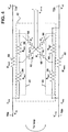
- FIG. 2 illustrates an exemplary serpentine resistance pattern 30 typically used to form R feed1 12 and R feed2 14 (FIG. 1) as part of a conventional telephony line card.
- Resistance pattern 30 is preferably etched using a resistive ink on a circuit board acting as a substrate, and forming the telephony line card.
- Each resistance pattern 30 preferably includes a vernier 32 (fine trim area); coarse trim area 34; and bulk resistance area 36 .
- a plurality of shorting links 38 allows for the adjustment of the resistance of coarse trim area 34 . By cutting any of the bottom shorting links 38 , the length of coarse trim area 34 , and hence its resistance and the resistance of pattern 30 is increased. Sequential cutting of additional bottom shorting links 38 allows for the additional adjustment of resistance of pattern 30.
- each of links 38 that is cut results in a step increase in the resistance of pattern 30 .
- Vernier 32 may be trimmed to incrementally adjust the resistance of pattern 30 in an amount less than the step increase effected by each link. Vernier 32 may be trimmed using conventional laser cuts. Because of the relatively low resistance value of vernier 32 , cuts in vernier 32 are not particularly sensitive to high voltage currents. Thus, by cutting links 38 and trimming vernier 32, the resistance of pattern 30 may be adjusted to a desired nominal, predetermined value so that current through it may easily be sensed, using circuit 10 of FIG. 1.
- serpentine resistance pattern 30 is trimmed after manufacture by laser cutting one or more of shorting links 38 thereby lengthening the effective end to end length of the serpentine resistance pattern 30 , so that it assumes a desired nominal value.
- resistance pattern 30 is, however, typically designed and etched with the assumption that, in some cases, no shorting link 38 will be cut. In such cases, the entire surge is absorbed in bulk resistance area 36 . Thus, bulk resistance area 36 typically assumes the majority of the surface area of resistance pattern 30 .
- bulk resistance area 36 usually occupies about 56% of the area of resistance pattern 30 ; coarse trim area 34 , 34%; and vernier 32 , 10%. This accordingly requires that the size of the substrate on which the resistance pattern 30 is etched be of an increased size. Clearly, by eliminating or reducing the size of coarse trim area 34 , the overall area occupied by resistance pattern 30 may be reduced.
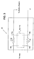
- FIG. 3 illustrates a line interface card 46 , including an enhanced voltage sensing circuit 40 or circuit 110, each exemplary of an embodiment of the present invention.
- Sensing circuit 40 is illustrated in FIG. 4 .
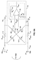
- Sensing circuit 110 is illustrated in FIG. 6A .
- circuit 40 may be used to sense a differential voltage across feed resistors R' feed1 50 and R' feed2 52 and hence a current attributable to differential voltage signals V' tip and V' ring at nodes 70b and 70b provided through feed resistors R' feed1 50 and R' feed2 52 .
- current sensing circuit 40 of FIG. 4 includes four sense resistors R' 1 62, R' 2 64, R' 3 66, and R'4 68, acting as a differentiating circuit.
- circuit 40 includes two voltage dividing circuits 42 and 44, each including two tap resistors R tap1 54, Rt ap2 56, and R tap3 58, R tap4 60, respectively.
- the differentiating circuit including sense resistors R' 1 62, R' 2 64, R' 3 66 and R' 4 68 are connected to voltage dividing circuits 42 and 44 across R tap2 56 and R tap4 60.
- the series combination of R tap1 54 and R tap2 56 is connected across R' feed1 50 .
- the series combination of R tap3 58 and R tap4 60 is connected across R' feed2 52.
- a further first series combination of R' 1 62 and R' 3 66 is connected to the end of R tap4 60 that is connected to input node 72b .
- the opposite end of the first series combination is connected to an end of R tap2 56 that is connected to R tap1 54.
- a second series combination of R' 2 64 and R' 4 68 is connected between the end of R tap2 56 connected to R tap1 54 and the end of R tap4 60 connected to input terminal 72b.
- V rtap2 V feed * R tap2 / (R tap1 + R tap2 ) .
- V rtap4 V feed * R tap4 / (R tap3 + R tap4 ) where V feed represents the voltage across feed resistor R feed1 .
- circuit 40 allows measurement of the desired current I' sense using the same sense amplifier used with the circuit 10 , without requiring knowledge of the nominal value of R' feed1 50 and R' feed2 52 provided that voltage sense circuit 40 including voltage dividing circuits 42 and 44 is properly matched to R' feed1 50 and R' feed2 52 .
- R' feed1 50 and R' feed2 52 may be extremely convenient.
- R tap1 54, R tap2 56, R tap3 58 and R tap4 60 may be formed as low power rectilinear resistors, that may be etched on a relatively small substrate.
- these low-power resistances may be easily adjusted through laser trimming.
- one of R' feed1 50 and R' feed2 52 may be measured and laser trimmed to be equal in value to the other one of R' feed1 50 and R' feed2 52 .
- a coarse trim area such as coarse trim area 34 is not necessarily required.
- R' feed1 50 and R' feed2 52 are formed during the same manufacturing process, their value will typically not differ by much from each other. As such, only a much smaller fine trim area will typically be necessary. This single fine trim area need only occupy 10% of the space occupied by the etched resistors R' feed1 50 and R' feed2 52. Moreover without a need for coarse trim area 34, R' feed1 50 and R' feed2 52 could be formed as rectilinear etched resistors.
- R' feed1 50 or R' feed2 52 is trimmed voltage sense circuits 42 and 44 may be tuned.
- R tap1 54, R tap2 56, R tap3 58, and R tap4 60 may be measured, R tap2 56 and R tap4 60 may be laser trimmed so that
- R tap1 54, R tap2 56, R tap3 58 and R tap4 60 may be laser trimmed so that
- R tap2 /(R tap1 + R tap2 ) I K
- the series combination of R tap1 54 and R tap2 56 and the series combination of R tap3 58 and R tap4 60 may be entirely eliminated by choosing an appropriate laser trim on a rectilinear resistor 80, used to form R' feed1 50 or R' feed2 52 of FIG. 4 as illustrated in FIG. 5 .
- resistor 80 may etched on a substrate using a resistive ink, and may then be trimmed to a desired resistance.
- a resistance at a sensepoint C located on body portion 86 between terminals 82 and 84 may be adjusted so that the voltage at sensepoint C equals the voltage across the resistor 80, divided by some known multiple of the resistance between terminals 82 and 84 .
- resistor 80 effectively includes its own voltage dividing circuit, equivalent to voltage dividing circuit 42 or 44 .
- resistance at sensepoint C may be adjusted by conventional laser trims along the body portion 86 . Specifically, by iteratively trimming body portion 86 on one or both sides of sensepoint C, the overall resistance of resistor 80 may be adjusted, and the relative voltage at sensepoint C may be adjusted.
- the voltage at sensepoint C may be connected by way of sense resistors, such as resistors R' 1 62 , R' 2 64 , R' 3 66 and R' 4 68 ( FIG. 4 ) to one of the inputs of a differential sense amplifier.
- sense resistors such as resistors R' 1 62 , R' 2 64 , R' 3 66 and R' 4 68 ( FIG. 4 ) to one of the inputs of a differential sense amplifier.
- Sense resistors R' 1 62 , R' 2 64 , R' 3 66 and R' 4 68 may similarly be formed as etched low power rectilinear resistors.
- R' 1 62, R' 2 64, R' 3 66 and R' 4 68 of circuit 40 may be trimmed so that the input impedance at the sense amplifier used in association with circuit 40 is identical to that of circuit 10 .
- R' 1 62, R' 2 64, R' 3 66 and R' 4 68 may be accomplished by trimming R' 1 62, R' 2 64, R' 3 66 and R' 4 68 so that the Thevenin equivalent resistance as sensed at terminals 74 and 76 is the same as the Thevenin resistance at the sense terminals of circuit 10 .
- This may, for example, be accomplished by shorting terminals 70a and 70b ; grounding terminals 72a and 72b ; measuring the input impedance at terminals 74 and 76 , and trimming R' 1 62 , R' 2 64 , R' 3 66 and R' 4 68 to provide the desired nominal Thevinin input impedance.
- the sense amplifier may be buffered so that the impedance of sensing circuit 40 does not affect the ultimate output of an interconnected sense amplifier.
- the above sense resistors are trimmed so that a sense amplifier generates a nominal output in proportion to the current attributable to the differential voltages across R' feed1 50 and R' feed2 52.
- Voltage sense circuit 40 formed in part by R tap1 54, R tap2 56, R tap3 58 and R tap4 60 is tuned so that the differential voltage provided to a sense amplifier is isolated from the actual nominal values of the R' feed1 50 and R' feed2 52 .
- the voltage sense circuit 110 of FIG. 6A is substantially identical to that illustrated in FIG. 1. It includes sense resistors R" 1 116 , R" 2 118, R" 3 120, and R" 4 122 connected in a bridge across R' feed1 50 and R' feed2 52 and thereby sensing voltage across R' feed1 50 and R' feed2 52. Further illustrated in FIG. 6A is a differential sense amplifier 100 (not specifically illustrated in FIGS. 1, 3 or 4 ).
- Example differential amplifier 100 includes a conventional operational amplifier 108, having resistor R a2 98 connected between its output and inverting input, and resistor R a1 96 connected between its non-inverting input and ground.
- the gain of amplifier 100 may be adjusted by adjusting amplifier resistors R a1 96 and R a2 98 so that the output of amplifier 108 equals the current through R' feed1 50 or R' feed2 52 , scaled by a known factor K.
- trimming R a1 96 and R a2 98 so that the output of differential amplifier 108 presents a gain of K/R' feed1 , a nominal value of R' feed1 50 and R' feed2 52 is not required.
- amplifier 108 is tuned so that its output voltage, V amp, equals, K/R" feed1 * ⁇ 1 ⁇ 2 [V tip - V in1 ] - 1 ⁇ 2 [V ring - V in2 ] ⁇ .
- the amplifier of FIG. 6A is again illustrated in FIG. 6B .
- V amp R a2 /R a1 *V sense .
- R amp_in1 112 and R amp_in2 114 of FIG. 6B actually represent the Thevenin resistances at terminals 102 and 104 of FIG. 6A.
- circuit 110 of FIG. 6A is preferably formed by first measuring R' feed1 50; trimming R' feed2 52 to have an identical value; trimming R" 1 116 , R" 2 118, R" 3 120 and R" 4 122 to have equivalent values and to present a fixed input impedance at terminals 102 , and 104 . As noted, with reference to FIG. 4 , this may be accomplished by shorting terminals 70a and 70b , and measuring the input impedance to ground at terminals 102 and 104 .
- V amp K/R" feed1 *V sense providing the desired output at amplifier 100.
- R' feed1 50 and R' feed2 52 need only be equal to each other, they need not be greatly trimmed. They may thus be formed as rectilinear resistors, reducing the area occupied by R' feed1 50 and R' feed2 52. Moreover, R" 1 116 , R" 2 118, R" 3 120, R" 4 122 , R a1 96 and R a2 98 may all be formed as low power rectilinear resistors, and trimmed to have the desired/required values.
- any differential gain stage adjusted so that its output is proportional to the differential voltage sensed across R' feed1 50 or R' feed2 52 in some known manner may achieve the same result.
- a further amplifier tuned to provide a net output in proportion to the sensed voltage could be connected in series with the output of the amplifier of FIG. 1. Numerous other ways to tune the amplifier and sense circuit will be understood by those of ordinary skill in the art.
- a person skilled in the art will readily appreciate any number of circuits that may be used to output a signal representative of a differential voltage across feed resistors R' feed1 50 and R' feed2 52.
Landscapes
- Physics & Mathematics (AREA)
- General Physics & Mathematics (AREA)
- Measurement Of Current Or Voltage (AREA)
- Apparatuses And Processes For Manufacturing Resistors (AREA)
- Interface Circuits In Exchanges (AREA)
Abstract
Description
Claims (26)
- A sensing circuit for measuring current through an impedance, comprising:
a voltage dividing circuit, for connection across said impedance, said voltage dividing circuit comprising a tap to provide a voltage proportional to a voltage across said impedance, divided by a factor equal to a known multiple of said impedance. - The sensing circuit of claim 1, wherein said known multiple equals one.
- The sensing circuit of claim 2, wherein said voltage dividing circuit comprises:
a first tap impedance connected in series with a second tap impedance and connected across said impedance, wherein a value of a ratio of said sum of said first tap impedance and said second tap impedance to said first tap impedance equals a value of said impedance. - The sensing circuit of claim 0, wherein said impedance comprises a resistance.
- The sensing circuit of claim 4, wherein said resistance comprises an etched pattern on a substrate.
- The sensing circuit of claim 5, wherein said first tap impedance comprises a resistance formed as a second etched pattern on said substrate, and said second tap resistance comprises a resistance formed as an third etched pattern on said substrate.
- The sensing circuit of claim 4, wherein said etched pattern is generally rectilinear.
- A sensing circuit for sensing current due to a differential voltage across first and second impedances, said sensing circuit comprising:a first voltage dividing circuit, for connection across said first impedance, said first voltage dividing circuit comprising a tap to provide a first voltage proportional to a voltage across said first impedance, divided by a factor equal to a known multiple of said first impedance;a second voltage dividing circuit, for connection across said second impedance, said second voltage dividing circuit comprising a tap to provide a second voltage proportional to a voltage across said second impedance, divided by a factor equal to said known multiple of said second impedance;a differentiating circuit, connected to said first voltage dividing circuit and said second voltage dividing circuit, to produce an output proportional to a difference of said first voltage and said second voltage.
- The current sensing circuit of claim 8, wherein said known multiple equals one.
- The sensing circuit of claim 8, wherein said first voltage dividing circuit comprises:
a first tap impedance connected in series with a second tap impedance and connected across said first impedance, wherein a value of a ratio of said sum of said first tap impedance and said second tap impedance to said first tap impedance equals a value of said first impedance. - The sensing circuit of claim 10, wherein said second voltage dividing circuit comprises:
a third tap impedance connected in series with a fourth tap impedance and connected across said second impedance, wherein a value of a ratio of said sum of said third tap impedance and said fourth tap impedance to said third tap impedance equals a value of said second impedance. - The sensing circuit of claim 11, wherein said differentiating circuit comprises:
a bridge circuit comprising:first, second third and fourth sense resistors;said first and third sense resistors connected in series to form a first series combination, said first series combination connected betweeni) an end of said first tap impedance that is connected to said second tap impedance; andii) an end of said fourth tap impedance that is connected to said second impedance;said second and fourth sense resistors connected in series to form a second series combination, said second series combination connected betweeni) an end of said third tap impedance that is connected to said fourth tap impedance; andii) an end of said first tap impedance that is connected to said second impedance. - The sensing circuit of claim 12, wherein said first, second, third and fourth sense resistors are equal to each other.
- A telephony line interface card, including a sensing circuit as claimed in claim 8.
- An impedance comprising,a first terminal;a second terminal;a body portion defining an impedance between said first terminal and said second terminal;a voltage tap on said body portion, between said first terminal and said second terminal to provide a sensed voltage proportional to a voltage between said first terminal and said second terminal, divided by a factor equal to a known multiple of said impedance between said first and second terminals.
- The impedance of claim 15, wherein said body portion is formed as an etched pattern on a substrate.
- The impedance of claim 16, wherein said etched pattern is generally rectilinear.
- The impedance of claim 17, wherein said voltage tap is located at a position along a length of said body portion to provide said sensed voltage proportional to said voltage between said first terminal and said second terminal, divided by a factor equal to said impedance between said first and second terminals.
- The impedance of claim 15, wherein said known multiple equals one.
- A telephony line interface card, comprising an impedance as claimed in claim 15.
- A method of tuning a current sensing circuit for measuring a current attributable to a differential voltage across a first and second impedance, said current sensing circuit comprising:a voltage sense circuit for sensing said differential voltage;a differential amplifier connected with said voltage sense circuit to provide a signal proportional to said differential voltage;said method comprising:
tuning at least one of said voltage sense circuit and said differential amplifier, so that an output of said differential amplifier provides said signal in known proportion to said differential voltage, and thereby provides a signal in known proportion to said current. - The method of claim 21, wherein a gain of said differential amplifier is adjusted so that said differential amplifier provides a signal in known proportion to said differential voltage.
- The method of claim 22, wherein said amplifier comprises an operational amplifier, and said gain is adjusted by adjusting a feedback resistor between an input and output of said operational amplifier.
- The method of claim 23, wherein said gain of said amplifier is based on a value of one of said first impedance and said second impedance.
- The method of claim 24, wherein said adjusting comprises measuring one of said first impedance and said second impedance.
- A telephony line interface card, including a current sensing circuit tuned in accordance with the method of claim 21.
Applications Claiming Priority (2)
| Application Number | Priority Date | Filing Date | Title |
|---|---|---|---|
| US47259499A | 1999-12-27 | 1999-12-27 | |
| US472594 | 2006-06-22 |
Publications (2)
| Publication Number | Publication Date |
|---|---|
| EP1126281A2 true EP1126281A2 (en) | 2001-08-22 |
| EP1126281A3 EP1126281A3 (en) | 2002-07-03 |
Family
ID=23876153
Family Applications (1)
| Application Number | Title | Priority Date | Filing Date |
|---|---|---|---|
| EP00310206A Withdrawn EP1126281A3 (en) | 1999-12-27 | 2000-11-16 | A current sensing circuit and telephone line interface card with enhanced current sensing circuit |
Country Status (2)
| Country | Link |
|---|---|
| EP (1) | EP1126281A3 (en) |
| CA (1) | CA2322934A1 (en) |
Families Citing this family (1)
| Publication number | Priority date | Publication date | Assignee | Title |
|---|---|---|---|---|
| US6795321B2 (en) | 2001-07-20 | 2004-09-21 | Power Integrations, Inc. | Method and apparatus for sensing current and voltage in circuits with voltage across an LED |
Family Cites Families (1)
| Publication number | Priority date | Publication date | Assignee | Title |
|---|---|---|---|---|
| US4514595A (en) * | 1982-06-10 | 1985-04-30 | Northern Telecom Limited | Active impedance line feed circuit |
-
2000
- 2000-10-11 CA CA 2322934 patent/CA2322934A1/en not_active Abandoned
- 2000-11-16 EP EP00310206A patent/EP1126281A3/en not_active Withdrawn
Also Published As
| Publication number | Publication date |
|---|---|
| CA2322934A1 (en) | 2001-06-27 |
| EP1126281A3 (en) | 2002-07-03 |
Similar Documents
| Publication | Publication Date | Title |
|---|---|---|
| US5486791A (en) | Programmable gain amplifier | |
| EP2273677B1 (en) | Wide bandwidth attenuator input circuit for a measurement probe | |
| US6362614B2 (en) | Electronic probe for measuring high impedance tri-state logic circuits | |
| US6608536B2 (en) | Constant impedance filter | |
| JP3629346B2 (en) | Signal transmission system and transmission line drive circuit | |
| US4088843A (en) | Electronic current feed circuit | |
| US4467296A (en) | Integrated electronic controlled diode filter microwave networks | |
| WO1999053613A1 (en) | Attenuating volume control | |
| US6204712B1 (en) | Method and apparatus for clock uncertainty minimization | |
| JPH10271043A (en) | Analog signal transmission circuit | |
| CA2322934A1 (en) | Current sensing circuit and telephone line interface card with enhanced current sensing circuit | |
| SE441560B (en) | HYBRID CIRCUIT | |
| WO1993021723A1 (en) | Impedance synthesizer for a subscriber line interface circuit | |
| US3983504A (en) | Active filter | |
| US7352259B2 (en) | Broadband step attenuator with improved time domain performance | |
| JP3131342B2 (en) | High frequency detection circuit | |
| US5614873A (en) | Electronic circuit | |
| US20020039413A1 (en) | ADSL front-end in a low voltage process that accommodates large line voltages | |
| EP0280516A2 (en) | Differential amplifier circuit | |
| DE3014187A1 (en) | CIRCUIT ARRANGEMENT FOR THE TWO-WIRE CONNECTION OF A TELEPHONE SUBSCRIBER TO A CABLE FOR IN- AND INPUT SIGNALS | |
| JPS646564B2 (en) | ||
| AU709973B2 (en) | Linear time invariant electrical system | |
| KR100257529B1 (en) | Frequency characteristics measuring apparatus for a high frequency filter | |
| JP2006065559A (en) | Transmission path characteristics matching method, interface circuit, electronic circuit, and transmission path characteristics matching program | |
| JP2730107B2 (en) | Current mirror circuit |
Legal Events
| Date | Code | Title | Description |
|---|---|---|---|
| PUAI | Public reference made under article 153(3) epc to a published international application that has entered the european phase |
Free format text: ORIGINAL CODE: 0009012 |
|
| AK | Designated contracting states |
Kind code of ref document: A2 Designated state(s): AT BE CH CY DE DK ES FI FR GB GR IE IT LI LU MC NL PT SE TR |
|
| AX | Request for extension of the european patent |
Free format text: AL;LT;LV;MK;RO;SI |
|
| PUAL | Search report despatched |
Free format text: ORIGINAL CODE: 0009013 |
|
| AK | Designated contracting states |
Kind code of ref document: A3 Designated state(s): AT BE CH CY DE DK ES FI FR GB GR IE IT LI LU MC NL PT SE TR |
|
| AX | Request for extension of the european patent |
Free format text: AL;LT;LV;MK;RO;SI |
|
| RIC1 | Information provided on ipc code assigned before grant |
Free format text: 7G 01R 19/15 A, 7G 01R 1/20 B, 7G 01R 19/00 B |
|
| 17P | Request for examination filed |
Effective date: 20021205 |
|
| AKX | Designation fees paid |
Designated state(s): DE FR GB |
|
| RAP1 | Party data changed (applicant data changed or rights of an application transferred) |
Owner name: NORTEL NETWORKS LIMITED |
|
| 17Q | First examination report despatched |
Effective date: 20040316 |
|
| STAA | Information on the status of an ep patent application or granted ep patent |
Free format text: STATUS: THE APPLICATION IS DEEMED TO BE WITHDRAWN |
|
| 18D | Application deemed to be withdrawn |
Effective date: 20040928 |