EP1124407B1 - Socket for BGA packages - Google Patents
Socket for BGA packages Download PDFInfo
- Publication number
- EP1124407B1 EP1124407B1 EP01301095A EP01301095A EP1124407B1 EP 1124407 B1 EP1124407 B1 EP 1124407B1 EP 01301095 A EP01301095 A EP 01301095A EP 01301095 A EP01301095 A EP 01301095A EP 1124407 B1 EP1124407 B1 EP 1124407B1
- Authority
- EP
- European Patent Office
- Prior art keywords
- socket
- contact assembly
- frame
- circuit board
- contact
- Prior art date
- Legal status (The legal status is an assumption and is not a legal conclusion. Google has not performed a legal analysis and makes no representation as to the accuracy of the status listed.)
- Expired - Lifetime
Links
- 230000014759 maintenance of location Effects 0.000 claims abstract description 5
- 239000011810 insulating material Substances 0.000 claims abstract description 3
- 230000002093 peripheral effect Effects 0.000 claims description 3
- 230000006835 compression Effects 0.000 claims description 2
- 238000007906 compression Methods 0.000 claims description 2
- 230000000717 retained effect Effects 0.000 abstract description 8
- 230000007246 mechanism Effects 0.000 abstract description 6
- 238000010276 construction Methods 0.000 abstract description 2
- 239000012212 insulator Substances 0.000 description 7
- 229910000831 Steel Inorganic materials 0.000 description 1
- 239000000463 material Substances 0.000 description 1
- 239000010959 steel Substances 0.000 description 1
Images




Classifications
-
- H—ELECTRICITY
- H05—ELECTRIC TECHNIQUES NOT OTHERWISE PROVIDED FOR
- H05K—PRINTED CIRCUITS; CASINGS OR CONSTRUCTIONAL DETAILS OF ELECTRIC APPARATUS; MANUFACTURE OF ASSEMBLAGES OF ELECTRICAL COMPONENTS
- H05K7/00—Constructional details common to different types of electric apparatus
- H05K7/02—Arrangements of circuit components or wiring on supporting structure
- H05K7/10—Plug-in assemblages of components, e.g. IC sockets
- H05K7/1053—Plug-in assemblages of components, e.g. IC sockets having interior leads
- H05K7/1061—Plug-in assemblages of components, e.g. IC sockets having interior leads co-operating by abutting
Definitions
- BGA ball grid array
- an electronic circuit typically an integrated circuit
- Such a package is typically mounted to a corresponding array of contact areas of a printed circuit board. Since the BGA package is soldered directly to a circuit board, the package is not removable from the board without unsoldering.
- Sockets are known for removably mounting electronic circuit packages onto printed circuit boards, see for example prior art document EP 0 706 312; however, sockets for BGA packages have not heretofore been successfully implemented. Test sockets are known for testing BGA packages but such test sockets are generally complex and relatively large and cumbersome and are impractical for use in usual circuit board environments.
- a socket for a BGA package as defined in claim 1 which is of relatively simple construction and which provides reliable and efficient interconnection of a BGA package and a printed circuit board.
- the socket comprises a contact assembly having an array of resilient conductive columns having respective contact ends, the columns being mounted on a thin insulative sheet.
- the contact assembly is supported on a frame of insulating material and which has alignment posts for alignment of the contact assembly to the frame and for alignment of the frame and mounted contact assembly to an associated circuit board.
- the frame also includes latch elements for retaining the contact assembly on the frame.
- the socket is mounted onto a printed circuit board which has an array of contact areas corresponding to the array of resilient contacts of the socket.
- a BGA package is placed onto the socket frame and the package is maintained in alignment on the frame such that the ball contacts engage the respective contacts of the contact assembly of the socket.
- the package is retained in the socket by a retention mechanism.
- the socket can include elements for preventing overstress of the resilient contacts.
- a socket for a BGA package which includes an insulator frame 10 and a contact assembly 12 retained in the frame.
- the contact assembly is adapted to be disposed on a printed circuit board and to be retained thereon by the insulator frame and a retention mechanism.
- a BGA package 14 (Fig. 7) is disposed on the insulator frame and is retained therein for electrical contact via the contact assembly to contacts on the circuit board.
- the socket 11 in relation to a circuit board 13 is shown in Fig. 8.
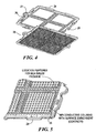
- the insulator frame 10 is of square or rectangular configuration in the illustrated embodiment and having a peripheral portion 16 and cross members 18 which contain an array of openings 20 which correspond to the configuration of contacts 22 on the contact assembly 12.
- the insulator frame also includes a plurality of snap clips 24 spaced about the periphery of the frame and locating posts 26 on respective sides of the frame.
- the locating posts are cooperative with respective openings 28 in the contact assembly and are also cooperative with openings in the circuit, board to which the socket is mounted for alignment of the socket to the circuit board.
- the locating posts have two different diameters as illustrated to provide proper orientation of the contact assembly on the frame and circuit board.
- the location posts 26 each have a first diameter 27 sized to which are stepped to locate the contact assembly 12 to the insulator frame 10, and a smaller diameter 29 to locate the socket to the printed circuit board.
- the contact assembly 12 is comprised of an insulating sheet 30 having an array of resilient conductive columns 32 disposed in respective openings through the sheet and having upper and lower contact ends.
- the conductive columns are preferably as shown in copending European Patent Application No 99310568.3 published on 30th August 2000 as EP-A-1032079 in the name of Thomas & Betts International, Inc..
- the contact assembly also includes stop posts 34 disposed between columns 32 to limit the amount of compression of the resilient conductive columns when the socket is mounted on a circuit board.
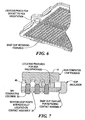
- the BGA package 14 is disposed in the socket with the ball contacts 40 in engagement with the contact ends of the contact assembly 12.
- Some of the ball contacts are disposed in openings 25 in the frame 10 which serve to align the ball contacts with the contact ends of the contact assembly 12.
- the ball contacts 40 of the BGA package each contact a respective contact end 32 of a conductive column of the contact assembly.
- the bottom contact ends 32 of the conductive columns engage respective contacts on the circuit board.
- the socket and BGA package are retained on a circuit board, in a preferred embodiment as shown in Fig. 9.
- the socket 11 is disposed on a circuit board 13 and retained in position by alignment or locating posts on the socket and cooperative openings on the circuit board as described above.
- a backing plate 50 is of generally rigid material such as steel and is disposed on the backside of the circuit board and insulated therefrom by an insulator plate 52.
- a heat sink 54 is disposed over the package 14 and the assembly is retained by a multi-beam spring 56 which fits in opening 57, and threaded fasteners 58 which are cooperative with threaded openings in the backing plate 50 to clamp the components together.
- This clamp mechanism is itself the subject of co-pending European Patent Application No (00304913.7 published on 13th December 2000 as EP-A-1059665 in the name of Thomas & Betts International, Inc..
- Other clamp or retention mechanisms may be employed to retain the socket and its circuit package on an associated circuit board.
Landscapes
- Engineering & Computer Science (AREA)
- Microelectronics & Electronic Packaging (AREA)
- Connecting Device With Holders (AREA)
Abstract
Description
- One well known form of electronic package is the ball grid array (BGA) package in which an electronic circuit, typically an integrated circuit, is contained within a thin rectangular housing having an array of ball shaped electrical contacts on a surface of the package. Such a package is typically mounted to a corresponding array of contact areas of a printed circuit board. Since the BGA package is soldered directly to a circuit board, the package is not removable from the board without unsoldering. Sockets are known for removably mounting electronic circuit packages onto printed circuit boards, see for example prior art document EP 0 706 312; however, sockets for BGA packages have not heretofore been successfully implemented. Test sockets are known for testing BGA packages but such test sockets are generally complex and relatively large and cumbersome and are impractical for use in usual circuit board environments.
- In accordance with the present invention, a socket for a BGA package as defined in claim 1 is provided which is of relatively simple construction and which provides reliable and efficient interconnection of a BGA package and a printed circuit board. The socket comprises a contact assembly having an array of resilient conductive columns having respective contact ends, the columns being mounted on a thin insulative sheet. The contact assembly is supported on a frame of insulating material and which has alignment posts for alignment of the contact assembly to the frame and for alignment of the frame and mounted contact assembly to an associated circuit board. The frame also includes latch elements for retaining the contact assembly on the frame.
- For use, the socket is mounted onto a printed circuit board which has an array of contact areas corresponding to the array of resilient contacts of the socket. A BGA package is placed onto the socket frame and the package is maintained in alignment on the frame such that the ball contacts engage the respective contacts of the contact assembly of the socket. The package is retained in the socket by a retention mechanism. The socket can include elements for preventing overstress of the resilient contacts.
- The invention will be more fully understood from the following detailed description taken in conjunction with the accompanying drawings in which:
- Fig. 1 is a pictorial top view of a socket in accordance with the invention;
- Fig. 2 is a bottom pictorial view of the socket of Fig. 1;
- Fig. 3 is an exploded view illustrating the frame and contact assembly of the socket of Figs. 1 and 2;
- Fig. 4 is another exploded view of the frame and contact assembly;
- Fig. 5 is an enlarged cutaway pictorial view of the socket of the invention;
- Fig. 6 is an enlarged bottom pictorial view partially cutaway of the embodiment of Fig. 6;
- Fig. 7 is an enlarged cross-sectional view illustrating a BGA package mounted on the socket;
- Fig. 8 is an exploded view of the socket of the invention and associated circuit board; and
- Fig. 9 is an exploded view of a clamp mechanism employed with the socket of the invention.
- Referring to the drawings there is shown a socket for a BGA package which includes an
insulator frame 10 and acontact assembly 12 retained in the frame. The contact assembly is adapted to be disposed on a printed circuit board and to be retained thereon by the insulator frame and a retention mechanism. A BGA package 14 (Fig. 7) is disposed on the insulator frame and is retained therein for electrical contact via the contact assembly to contacts on the circuit board. Thesocket 11 in relation to acircuit board 13 is shown in Fig. 8. - The
insulator frame 10 is of square or rectangular configuration in the illustrated embodiment and having aperipheral portion 16 andcross members 18 which contain an array ofopenings 20 which correspond to the configuration ofcontacts 22 on thecontact assembly 12. The insulator frame also includes a plurality ofsnap clips 24 spaced about the periphery of the frame and locatingposts 26 on respective sides of the frame. The locating posts are cooperative withrespective openings 28 in the contact assembly and are also cooperative with openings in the circuit, board to which the socket is mounted for alignment of the socket to the circuit board. The locating posts have two different diameters as illustrated to provide proper orientation of the contact assembly on the frame and circuit board. Thelocation posts 26 each have afirst diameter 27 sized to which are stepped to locate thecontact assembly 12 to theinsulator frame 10, and asmaller diameter 29 to locate the socket to the printed circuit board. - The
contact assembly 12 is comprised of aninsulating sheet 30 having an array of resilient conductive columns 32 disposed in respective openings through the sheet and having upper and lower contact ends. The conductive columns are preferably as shown in copending European Patent Application No 99310568.3 published on 30th August 2000 as EP-A-1032079 in the name of Thomas & Betts International, Inc.. The contact assembly also includes stop posts 34 disposed between columns 32 to limit the amount of compression of the resilient conductive columns when the socket is mounted on a circuit board. - As shown in Fig. 7, the
BGA package 14 is disposed in the socket with theball contacts 40 in engagement with the contact ends of thecontact assembly 12. Some of the ball contacts are disposed inopenings 25 in theframe 10 which serve to align the ball contacts with the contact ends of thecontact assembly 12. Theball contacts 40 of the BGA package each contact a respective contact end 32 of a conductive column of the contact assembly. The bottom contact ends 32 of the conductive columns engage respective contacts on the circuit board. - The socket and BGA package are retained on a circuit board, in a preferred embodiment as shown in Fig. 9. The
socket 11 is disposed on acircuit board 13 and retained in position by alignment or locating posts on the socket and cooperative openings on the circuit board as described above. Abacking plate 50 is of generally rigid material such as steel and is disposed on the backside of the circuit board and insulated therefrom by aninsulator plate 52. Aheat sink 54 is disposed over thepackage 14 and the assembly is retained by amulti-beam spring 56 which fits in opening 57, and threadedfasteners 58 which are cooperative with threaded openings in thebacking plate 50 to clamp the components together. This clamp mechanism is itself the subject of co-pending European Patent Application No (00304913.7 published on 13th December 2000 as EP-A-1059665 in the name of Thomas & Betts International, Inc.. Other clamp or retention mechanisms may be employed to retain the socket and its circuit package on an associated circuit board.
Claims (8)
- A socket (11) for a BGA package (14) comprising:a contact assembly (12) having an array of resilient conductive columns (32) having respective contact ends (22) and an insulative sheet (30) on which the conductive columns (32) are mounted; anda frame (10) of insulating material for retaining the contact assembly on a printed circuit board and having first elements (26, 27) for alignment of the frame to the contact assembly, second elements (26, 29) for alignment of the socket to an associated circuit board (13), and third elements for alignment of a BGA package on the socket, the frame includinga peripheral portion (16) having the third elements composed of an array of openings (20) which correspond to the configuration of the contact ends on the contact assembly, andat least one cross member (18) extending between sections of the peripheral portion and which have the third elements composed of an array of openings (20) which correspond to the configuration of the contact ends on the contact assembly.
- The socket of claim 1 wherein the frame includes snap clips (24) spaced about the periphery thereof and operative to retain the insulative sheet of the contact assembly on the frame.
- The socket of claim 1 or claim 2 wherein the first elements include locating posts (26) having a section of first diameter (27) cooperative with openings (28) in the contact assembly for retention of the contact assembly in alignment on the frame.
- The socket of claim 3 wherein the second elements include locating posts (26) having a section of second diameter (29) cooperative with respective openings in the associated circuit board for retaining the socket in aligned position on the circuit board.
- The socket of claim 1 or claim 2 wherein the second elements include locating posts (26) having portions of two different diameters, first portions of first diameter (27) cooperative with respective openings (28) in the contact assembly (12) and second portions of second diameter (29) being cooperative with respective openings in the associated circuit board.
- The socket of any one of claims 1 to 5 wherein the contact assembly includes the insulative sheet (30) having an array of openings in which the resilient conductive columns are respectively disposed.
- The socket of any one of claims 1 to 6 wherein the insulative sheet of the contact assembly includes stop posts (34) disposed between selected resilient conductive columns (32) and operative to limit the amount of compression of the resilient conductive columns (32) when the socket (11) is mounted on the circuit board.
- The socket of any one of claims 1 to 7 wherein the third elements are openings (25) in at least a portion of the frame which contain the contact ends (32) of the contact assembly (12) and which are operative to align a BGA package (14) on the socket (11).
Applications Claiming Priority (2)
| Application Number | Priority Date | Filing Date | Title |
|---|---|---|---|
| US499772 | 1983-05-31 | ||
| US09/499,772 US6293810B1 (en) | 2000-02-08 | 2000-02-08 | Socket for BGA packages |
Publications (3)
| Publication Number | Publication Date |
|---|---|
| EP1124407A2 EP1124407A2 (en) | 2001-08-16 |
| EP1124407A3 EP1124407A3 (en) | 2003-05-14 |
| EP1124407B1 true EP1124407B1 (en) | 2006-01-04 |
Family
ID=23986637
Family Applications (1)
| Application Number | Title | Priority Date | Filing Date |
|---|---|---|---|
| EP01301095A Expired - Lifetime EP1124407B1 (en) | 2000-02-08 | 2001-02-07 | Socket for BGA packages |
Country Status (5)
| Country | Link |
|---|---|
| US (1) | US6293810B1 (en) |
| EP (1) | EP1124407B1 (en) |
| JP (1) | JP4791639B2 (en) |
| AT (1) | ATE315327T1 (en) |
| DE (1) | DE60116437T2 (en) |
Families Citing this family (13)
| Publication number | Priority date | Publication date | Assignee | Title |
|---|---|---|---|---|
| US6945788B2 (en) * | 2003-07-31 | 2005-09-20 | Tyco Electronics Corporation | Metal contact LGA socket |
| US6881073B2 (en) * | 2003-08-12 | 2005-04-19 | Cinch Connectors, Inc. | Electrical connector |
| US7059869B2 (en) * | 2004-02-27 | 2006-06-13 | Tyco Electronics Corporation | Metal contact LGA socket |
| KR100602442B1 (en) * | 2004-05-18 | 2006-07-19 | 삼성전자주식회사 | Test Sockets for Ball Grid Array Packages with Intermediate Boards |
| US7442049B2 (en) * | 2005-02-09 | 2008-10-28 | International Business Machines Corporation | Electrical connecting device and method of forming same |
| USD541748S1 (en) * | 2005-03-07 | 2007-05-01 | Cheng Uei Precision Industry Co., Ltd. | Board to board receptacle connector |
| USD540258S1 (en) * | 2005-03-07 | 2007-04-10 | Cheng Uei Precision Industry Co., Ltd. | Board to board plug connector |
| US7331796B2 (en) * | 2005-09-08 | 2008-02-19 | International Business Machines Corporation | Land grid array (LGA) interposer utilizing metal-on-elastomer hemi-torus and other multiple points of contact geometries |
| KR100974586B1 (en) | 2007-12-31 | 2010-08-06 | 이성재 | BK Semiconductor Test Socket |
| JP1618358S (en) * | 2018-04-23 | 2018-11-19 | ||
| JP1618359S (en) * | 2018-04-23 | 2018-11-19 | ||
| DE102020005363A1 (en) * | 2019-09-12 | 2021-03-18 | Sew-Eurodrive Gmbh & Co Kg | Electrical device and method for producing a first and second electrical device from a kit |
| USD949799S1 (en) * | 2020-06-09 | 2022-04-26 | Yamaichi Electronics Co., Ltd. | Mezzanine connector housing |
Family Cites Families (17)
| Publication number | Priority date | Publication date | Assignee | Title |
|---|---|---|---|---|
| US4239312A (en) * | 1978-11-29 | 1980-12-16 | Hughes Aircraft Company | Parallel interconnect for planar arrays |
| FR2669149B1 (en) * | 1990-11-12 | 1994-09-02 | Souriau & Cie | INTERMEDIATE CONNECTOR BETWEEN PRINTED CIRCUIT BOARD AND SUBSTRATE WITH ACTIVE ELECTRONIC CIRCUITS. |
| US5155905A (en) * | 1991-05-03 | 1992-10-20 | Ltv Aerospace And Defense Company | Method and apparatus for attaching a circuit component to a printed circuit board |
| US5163837A (en) * | 1991-06-26 | 1992-11-17 | Amp Incorporated | Ordered area array connector |
| US5302853A (en) * | 1993-01-25 | 1994-04-12 | The Whitaker Corporation | Land grid array package |
| US5344334A (en) * | 1993-06-11 | 1994-09-06 | The Whitaker Corporation | Hinged cover for an electrical socket |
| US5599193A (en) * | 1994-08-23 | 1997-02-04 | Augat Inc. | Resilient electrical interconnect |
| US5713744A (en) * | 1994-09-28 | 1998-02-03 | The Whitaker Corporation | Integrated circuit socket for ball grid array and land grid array lead styles |
| NL9401658A (en) * | 1994-10-07 | 1996-05-01 | Framatome Connectors Belgium | Connector for a substrate with an electronic circuit. |
| JPH0935789A (en) * | 1995-07-21 | 1997-02-07 | Shin Etsu Polymer Co Ltd | Anisotropic conductive sheet and its manufacture |
| US5730620A (en) * | 1995-09-08 | 1998-03-24 | International Business Machines Corporation | Method and apparatus for locating electrical circuit members |
| TW383951U (en) * | 1996-01-23 | 2000-03-01 | Whitaker Corp | Electrical connector for connecting electronic package to circuit board |
| US5738531A (en) * | 1996-09-09 | 1998-04-14 | International Business Machines Corporation | Self-alligning low profile socket for connecting ball grid array devices through a dendritic interposer |
| US5919050A (en) * | 1997-04-14 | 1999-07-06 | International Business Machines Corporation | Method and apparatus for separable interconnecting electronic components |
| JPH11176545A (en) * | 1997-12-12 | 1999-07-02 | Pfu Ltd | BGA socket adapter |
| JPH11271392A (en) * | 1998-03-25 | 1999-10-08 | Machine Active Contact:Kk | Carrier socket structural body |
| US6114757A (en) * | 1999-09-27 | 2000-09-05 | Thomas & Betts International, Inc. | Leadless IC socket |
-
2000
- 2000-02-08 US US09/499,772 patent/US6293810B1/en not_active Expired - Lifetime
-
2001
- 2001-02-07 AT AT01301095T patent/ATE315327T1/en not_active IP Right Cessation
- 2001-02-07 DE DE60116437T patent/DE60116437T2/en not_active Expired - Lifetime
- 2001-02-07 EP EP01301095A patent/EP1124407B1/en not_active Expired - Lifetime
- 2001-02-08 JP JP2001032489A patent/JP4791639B2/en not_active Expired - Fee Related
Also Published As
| Publication number | Publication date |
|---|---|
| JP4791639B2 (en) | 2011-10-12 |
| DE60116437T2 (en) | 2006-08-03 |
| DE60116437D1 (en) | 2006-03-30 |
| JP2001257050A (en) | 2001-09-21 |
| ATE315327T1 (en) | 2006-02-15 |
| EP1124407A3 (en) | 2003-05-14 |
| EP1124407A2 (en) | 2001-08-16 |
| US6293810B1 (en) | 2001-09-25 |
Similar Documents
| Publication | Publication Date | Title |
|---|---|---|
| US6400577B1 (en) | Integrated circuit socket assembly having integral shielding members | |
| US5296652A (en) | Apparatus for attaching a circuit component to a printed circuit board | |
| US5131852A (en) | Electrical socket | |
| US7632128B2 (en) | Electrical connector assembly with fastening element | |
| US6293810B1 (en) | Socket for BGA packages | |
| US6114757A (en) | Leadless IC socket | |
| US6375476B1 (en) | LGA package socket | |
| JP2004103407A (en) | Socket for electrical component | |
| US20070254500A1 (en) | Socket connector | |
| US6811407B2 (en) | Socket for electrical parts | |
| US7884630B2 (en) | IC carrie, IC socket and method for testing IC device | |
| US6659795B1 (en) | Electrical connector with retention posts | |
| JP2001244599A (en) | Ic mounting structure and position fixing sheet for bga type ic | |
| US6164981A (en) | Package socket system | |
| JP3694165B2 (en) | IC socket | |
| TW549724U (en) | Ball grid array socket | |
| US6461168B2 (en) | Plug socket for a display instrument | |
| JPH0878867A (en) | PCB fixing metal fittings for electrical equipment | |
| US6790069B2 (en) | IC socket with resistant mechanism | |
| US20080237020A1 (en) | Switch device having a spacer organizing contact tails | |
| JP4142222B2 (en) | Semiconductor device holder | |
| KR101034803B1 (en) | Socket for attaching electronic parts | |
| JP2576335Y2 (en) | Leaf switch | |
| JP3701738B2 (en) | Electrical connector | |
| JPH06103799B2 (en) | Device for shielding components with multi-pole plugs |
Legal Events
| Date | Code | Title | Description |
|---|---|---|---|
| PUAI | Public reference made under article 153(3) epc to a published international application that has entered the european phase |
Free format text: ORIGINAL CODE: 0009012 |
|
| AK | Designated contracting states |
Kind code of ref document: A2 Designated state(s): AT BE CH CY DE DK ES FI FR GB GR IE IT LI LU MC NL PT SE TR |
|
| AX | Request for extension of the european patent |
Free format text: AL;LT;LV;MK;RO;SI |
|
| RAP1 | Party data changed (applicant data changed or rights of an application transferred) |
Owner name: THOMAS & BETTS INTERNATIONAL, INC. |
|
| PUAL | Search report despatched |
Free format text: ORIGINAL CODE: 0009013 |
|
| AK | Designated contracting states |
Designated state(s): AT BE CH CY DE DK ES FI FR GB GR IE IT LI LU MC NL PT SE TR |
|
| AX | Request for extension of the european patent |
Extension state: AL LT LV MK RO SI |
|
| RIC1 | Information provided on ipc code assigned before grant |
Ipc: 7H 01R 13/24 B Ipc: 7H 05K 7/10 A |
|
| 17P | Request for examination filed |
Effective date: 20030911 |
|
| AKX | Designation fees paid |
Designated state(s): AT BE CH CY DE DK ES FI FR GB GR IE IT LI LU MC NL PT SE TR |
|
| GRAP | Despatch of communication of intention to grant a patent |
Free format text: ORIGINAL CODE: EPIDOSNIGR1 |
|
| GRAS | Grant fee paid |
Free format text: ORIGINAL CODE: EPIDOSNIGR3 |
|
| GRAA | (expected) grant |
Free format text: ORIGINAL CODE: 0009210 |
|
| AK | Designated contracting states |
Kind code of ref document: B1 Designated state(s): AT BE CH CY DE DK ES FI FR GB GR IE IT LI LU MC NL PT SE TR |
|
| PG25 | Lapsed in a contracting state [announced via postgrant information from national office to epo] |
Ref country code: AT Free format text: LAPSE BECAUSE OF FAILURE TO SUBMIT A TRANSLATION OF THE DESCRIPTION OR TO PAY THE FEE WITHIN THE PRESCRIBED TIME-LIMIT Effective date: 20060104 Ref country code: LI Free format text: LAPSE BECAUSE OF FAILURE TO SUBMIT A TRANSLATION OF THE DESCRIPTION OR TO PAY THE FEE WITHIN THE PRESCRIBED TIME-LIMIT Effective date: 20060104 Ref country code: FI Free format text: LAPSE BECAUSE OF FAILURE TO SUBMIT A TRANSLATION OF THE DESCRIPTION OR TO PAY THE FEE WITHIN THE PRESCRIBED TIME-LIMIT Effective date: 20060104 Ref country code: CH Free format text: LAPSE BECAUSE OF FAILURE TO SUBMIT A TRANSLATION OF THE DESCRIPTION OR TO PAY THE FEE WITHIN THE PRESCRIBED TIME-LIMIT Effective date: 20060104 Ref country code: BE Free format text: LAPSE BECAUSE OF FAILURE TO SUBMIT A TRANSLATION OF THE DESCRIPTION OR TO PAY THE FEE WITHIN THE PRESCRIBED TIME-LIMIT Effective date: 20060104 |
|
| REG | Reference to a national code |
Ref country code: GB Ref legal event code: FG4D |
|
| REG | Reference to a national code |
Ref country code: CH Ref legal event code: EP |
|
| PG25 | Lapsed in a contracting state [announced via postgrant information from national office to epo] |
Ref country code: IE Free format text: LAPSE BECAUSE OF NON-PAYMENT OF DUE FEES Effective date: 20060207 |
|
| REG | Reference to a national code |
Ref country code: IE Ref legal event code: FG4D |
|
| PG25 | Lapsed in a contracting state [announced via postgrant information from national office to epo] |
Ref country code: MC Free format text: LAPSE BECAUSE OF NON-PAYMENT OF DUE FEES Effective date: 20060228 |
|
| PG25 | Lapsed in a contracting state [announced via postgrant information from national office to epo] |
Ref country code: LU Free format text: LAPSE BECAUSE OF NON-PAYMENT OF DUE FEES Effective date: 20060304 |
|
| REF | Corresponds to: |
Ref document number: 60116437 Country of ref document: DE Date of ref document: 20060330 Kind code of ref document: P |
|
| PG25 | Lapsed in a contracting state [announced via postgrant information from national office to epo] |
Ref country code: SE Free format text: LAPSE BECAUSE OF FAILURE TO SUBMIT A TRANSLATION OF THE DESCRIPTION OR TO PAY THE FEE WITHIN THE PRESCRIBED TIME-LIMIT Effective date: 20060404 Ref country code: DK Free format text: LAPSE BECAUSE OF FAILURE TO SUBMIT A TRANSLATION OF THE DESCRIPTION OR TO PAY THE FEE WITHIN THE PRESCRIBED TIME-LIMIT Effective date: 20060404 |
|
| PG25 | Lapsed in a contracting state [announced via postgrant information from national office to epo] |
Ref country code: ES Free format text: LAPSE BECAUSE OF FAILURE TO SUBMIT A TRANSLATION OF THE DESCRIPTION OR TO PAY THE FEE WITHIN THE PRESCRIBED TIME-LIMIT Effective date: 20060415 |
|
| PG25 | Lapsed in a contracting state [announced via postgrant information from national office to epo] |
Ref country code: PT Free format text: LAPSE BECAUSE OF FAILURE TO SUBMIT A TRANSLATION OF THE DESCRIPTION OR TO PAY THE FEE WITHIN THE PRESCRIBED TIME-LIMIT Effective date: 20060605 |
|
| REG | Reference to a national code |
Ref country code: CH Ref legal event code: PL |
|
| ET | Fr: translation filed | ||
| PLBE | No opposition filed within time limit |
Free format text: ORIGINAL CODE: 0009261 |
|
| STAA | Information on the status of an ep patent application or granted ep patent |
Free format text: STATUS: NO OPPOSITION FILED WITHIN TIME LIMIT |
|
| 26N | No opposition filed |
Effective date: 20061005 |
|
| PG25 | Lapsed in a contracting state [announced via postgrant information from national office to epo] |
Ref country code: GR Free format text: LAPSE BECAUSE OF FAILURE TO SUBMIT A TRANSLATION OF THE DESCRIPTION OR TO PAY THE FEE WITHIN THE PRESCRIBED TIME-LIMIT Effective date: 20060405 |
|
| PG25 | Lapsed in a contracting state [announced via postgrant information from national office to epo] |
Ref country code: TR Free format text: LAPSE BECAUSE OF FAILURE TO SUBMIT A TRANSLATION OF THE DESCRIPTION OR TO PAY THE FEE WITHIN THE PRESCRIBED TIME-LIMIT Effective date: 20060104 |
|
| PG25 | Lapsed in a contracting state [announced via postgrant information from national office to epo] |
Ref country code: CY Free format text: LAPSE BECAUSE OF FAILURE TO SUBMIT A TRANSLATION OF THE DESCRIPTION OR TO PAY THE FEE WITHIN THE PRESCRIBED TIME-LIMIT Effective date: 20060104 |
|
| PGFP | Annual fee paid to national office [announced via postgrant information from national office to epo] |
Ref country code: IT Payment date: 20120224 Year of fee payment: 12 |
|
| PGFP | Annual fee paid to national office [announced via postgrant information from national office to epo] |
Ref country code: DE Payment date: 20130227 Year of fee payment: 13 Ref country code: FR Payment date: 20130311 Year of fee payment: 13 Ref country code: GB Payment date: 20130227 Year of fee payment: 13 |
|
| PGFP | Annual fee paid to national office [announced via postgrant information from national office to epo] |
Ref country code: NL Payment date: 20130224 Year of fee payment: 13 |
|
| REG | Reference to a national code |
Ref country code: DE Ref legal event code: R119 Ref document number: 60116437 Country of ref document: DE |
|
| REG | Reference to a national code |
Ref country code: NL Ref legal event code: V1 Effective date: 20140901 |
|
| GBPC | Gb: european patent ceased through non-payment of renewal fee |
Effective date: 20140207 |
|
| PG25 | Lapsed in a contracting state [announced via postgrant information from national office to epo] |
Ref country code: NL Free format text: LAPSE BECAUSE OF NON-PAYMENT OF DUE FEES Effective date: 20140901 |
|
| REG | Reference to a national code |
Ref country code: FR Ref legal event code: ST Effective date: 20141031 |
|
| REG | Reference to a national code |
Ref country code: DE Ref legal event code: R119 Ref document number: 60116437 Country of ref document: DE Effective date: 20140902 |
|
| PG25 | Lapsed in a contracting state [announced via postgrant information from national office to epo] |
Ref country code: GB Free format text: LAPSE BECAUSE OF NON-PAYMENT OF DUE FEES Effective date: 20140207 Ref country code: DE Free format text: LAPSE BECAUSE OF NON-PAYMENT OF DUE FEES Effective date: 20140902 Ref country code: FR Free format text: LAPSE BECAUSE OF NON-PAYMENT OF DUE FEES Effective date: 20140228 |
|
| PG25 | Lapsed in a contracting state [announced via postgrant information from national office to epo] |
Ref country code: IT Free format text: LAPSE BECAUSE OF NON-PAYMENT OF DUE FEES Effective date: 20140207 |