EP1122790B1 - A conductive mesh bias connection for an array of elevated active pixel sensors - Google Patents
A conductive mesh bias connection for an array of elevated active pixel sensors Download PDFInfo
- Publication number
- EP1122790B1 EP1122790B1 EP00122087A EP00122087A EP1122790B1 EP 1122790 B1 EP1122790 B1 EP 1122790B1 EP 00122087 A EP00122087 A EP 00122087A EP 00122087 A EP00122087 A EP 00122087A EP 1122790 B1 EP1122790 B1 EP 1122790B1
- Authority
- EP
- European Patent Office
- Prior art keywords
- layer
- conductive
- sensors
- pixel
- substrate
- Prior art date
- Legal status (The legal status is an assumption and is not a legal conclusion. Google has not performed a legal analysis and makes no representation as to the accuracy of the status listed.)
- Expired - Lifetime
Links
- 239000000758 substrate Substances 0.000 claims description 41
- 229910021417 amorphous silicon Inorganic materials 0.000 claims description 12
- WFKWXMTUELFFGS-UHFFFAOYSA-N tungsten Chemical compound [W] WFKWXMTUELFFGS-UHFFFAOYSA-N 0.000 claims description 11
- 229910052721 tungsten Inorganic materials 0.000 claims description 11
- 239000010937 tungsten Substances 0.000 claims description 11
- 229910052751 metal Inorganic materials 0.000 claims description 3
- 239000002184 metal Substances 0.000 claims description 3
- 239000007789 gas Substances 0.000 description 14
- 238000000034 method Methods 0.000 description 9
- 239000000463 material Substances 0.000 description 8
- XUIMIQQOPSSXEZ-UHFFFAOYSA-N Silicon Chemical compound [Si] XUIMIQQOPSSXEZ-UHFFFAOYSA-N 0.000 description 7
- 229910052710 silicon Inorganic materials 0.000 description 7
- 239000010703 silicon Substances 0.000 description 7
- 238000005229 chemical vapour deposition Methods 0.000 description 6
- ZOXJGFHDIHLPTG-UHFFFAOYSA-N Boron Chemical compound [B] ZOXJGFHDIHLPTG-UHFFFAOYSA-N 0.000 description 5
- 229910052796 boron Inorganic materials 0.000 description 5
- 239000004020 conductor Substances 0.000 description 5
- BHEPBYXIRTUNPN-UHFFFAOYSA-N hydridophosphorus(.) (triplet) Chemical compound [PH] BHEPBYXIRTUNPN-UHFFFAOYSA-N 0.000 description 5
- 238000004519 manufacturing process Methods 0.000 description 5
- RYGMFSIKBFXOCR-UHFFFAOYSA-N Copper Chemical compound [Cu] RYGMFSIKBFXOCR-UHFFFAOYSA-N 0.000 description 4
- 229910052782 aluminium Inorganic materials 0.000 description 4
- XAGFODPZIPBFFR-UHFFFAOYSA-N aluminium Chemical compound [Al] XAGFODPZIPBFFR-UHFFFAOYSA-N 0.000 description 4
- 229910052802 copper Inorganic materials 0.000 description 4
- 239000010949 copper Substances 0.000 description 4
- 238000000151 deposition Methods 0.000 description 4
- 230000000694 effects Effects 0.000 description 4
- 238000002955 isolation Methods 0.000 description 4
- 230000008021 deposition Effects 0.000 description 3
- 238000005530 etching Methods 0.000 description 3
- 230000010354 integration Effects 0.000 description 3
- 238000005546 reactive sputtering Methods 0.000 description 3
- 239000004065 semiconductor Substances 0.000 description 3
- UFHFLCQGNIYNRP-UHFFFAOYSA-N Hydrogen Chemical compound [H][H] UFHFLCQGNIYNRP-UHFFFAOYSA-N 0.000 description 2
- 230000009977 dual effect Effects 0.000 description 2
- 229910052739 hydrogen Inorganic materials 0.000 description 2
- 239000001257 hydrogen Substances 0.000 description 2
- 238000003384 imaging method Methods 0.000 description 2
- 230000000717 retained effect Effects 0.000 description 2
- 238000004544 sputter deposition Methods 0.000 description 2
- OKTJSMMVPCPJKN-UHFFFAOYSA-N Carbon Chemical compound [C] OKTJSMMVPCPJKN-UHFFFAOYSA-N 0.000 description 1
- 229910007264 Si2H6 Inorganic materials 0.000 description 1
- BLRPTPMANUNPDV-UHFFFAOYSA-N Silane Chemical compound [SiH4] BLRPTPMANUNPDV-UHFFFAOYSA-N 0.000 description 1
- 229910000577 Silicon-germanium Inorganic materials 0.000 description 1
- NRTOMJZYCJJWKI-UHFFFAOYSA-N Titanium nitride Chemical compound [Ti]#N NRTOMJZYCJJWKI-UHFFFAOYSA-N 0.000 description 1
- LEVVHYCKPQWKOP-UHFFFAOYSA-N [Si].[Ge] Chemical compound [Si].[Ge] LEVVHYCKPQWKOP-UHFFFAOYSA-N 0.000 description 1
- 229910003481 amorphous carbon Inorganic materials 0.000 description 1
- 230000004888 barrier function Effects 0.000 description 1
- 239000003610 charcoal Substances 0.000 description 1
- 239000003086 colorant Substances 0.000 description 1
- 230000000295 complement effect Effects 0.000 description 1
- 230000001143 conditioned effect Effects 0.000 description 1
- PZPGRFITIJYNEJ-UHFFFAOYSA-N disilane Chemical compound [SiH3][SiH3] PZPGRFITIJYNEJ-UHFFFAOYSA-N 0.000 description 1
- 239000007772 electrode material Substances 0.000 description 1
- 238000005516 engineering process Methods 0.000 description 1
- 230000008020 evaporation Effects 0.000 description 1
- 238000001704 evaporation Methods 0.000 description 1
- 229910052732 germanium Inorganic materials 0.000 description 1
- GNPVGFCGXDBREM-UHFFFAOYSA-N germanium atom Chemical compound [Ge] GNPVGFCGXDBREM-UHFFFAOYSA-N 0.000 description 1
- 229910044991 metal oxide Inorganic materials 0.000 description 1
- 150000004706 metal oxides Chemical class 0.000 description 1
- 150000004767 nitrides Chemical class 0.000 description 1
- 230000003287 optical effect Effects 0.000 description 1
- HBMJWWWQQXIZIP-UHFFFAOYSA-N silicon carbide Chemical compound [Si+]#[C-] HBMJWWWQQXIZIP-UHFFFAOYSA-N 0.000 description 1
- 239000007787 solid Substances 0.000 description 1
- 238000003860 storage Methods 0.000 description 1
- 238000007740 vapor deposition Methods 0.000 description 1
Images



Classifications
-
- H—ELECTRICITY
- H10—SEMICONDUCTOR DEVICES; ELECTRIC SOLID-STATE DEVICES NOT OTHERWISE PROVIDED FOR
- H10F—INORGANIC SEMICONDUCTOR DEVICES SENSITIVE TO INFRARED RADIATION, LIGHT, ELECTROMAGNETIC RADIATION OF SHORTER WAVELENGTH OR CORPUSCULAR RADIATION
- H10F39/00—Integrated devices, or assemblies of multiple devices, comprising at least one element covered by group H10F30/00, e.g. radiation detectors comprising photodiode arrays
- H10F39/10—Integrated devices
- H10F39/12—Image sensors
- H10F39/191—Photoconductor image sensors
-
- H—ELECTRICITY
- H10—SEMICONDUCTOR DEVICES; ELECTRIC SOLID-STATE DEVICES NOT OTHERWISE PROVIDED FOR
- H10F—INORGANIC SEMICONDUCTOR DEVICES SENSITIVE TO INFRARED RADIATION, LIGHT, ELECTROMAGNETIC RADIATION OF SHORTER WAVELENGTH OR CORPUSCULAR RADIATION
- H10F39/00—Integrated devices, or assemblies of multiple devices, comprising at least one element covered by group H10F30/00, e.g. radiation detectors comprising photodiode arrays
- H10F39/80—Constructional details of image sensors
-
- H—ELECTRICITY
- H10—SEMICONDUCTOR DEVICES; ELECTRIC SOLID-STATE DEVICES NOT OTHERWISE PROVIDED FOR
- H10F—INORGANIC SEMICONDUCTOR DEVICES SENSITIVE TO INFRARED RADIATION, LIGHT, ELECTROMAGNETIC RADIATION OF SHORTER WAVELENGTH OR CORPUSCULAR RADIATION
- H10F77/00—Constructional details of devices covered by this subclass
- H10F77/20—Electrodes
- H10F77/206—Electrodes for devices having potential barriers
Definitions
- This invention relates generally to photo diode active pixel sensors.
- it relates to a conductive mesh bias connection for an array of elevated active pixel sensors which provides light shielding between the active pixel sensors.
- An array of image sensors or light sensitive sensors detect the intensity of light received by the image sensors.
- the image sensors typically generate electronic signals that have amplitudes that are proportionate to the intensity of the light received by the image sensors.
- the image sensors can convert an optical image into a set of electronic signals.
- the electronic signals may represent intensities of colors of light received by the image sensors.
- the electronic signals can be conditioned and sampled to allow image processing.
- Integration of the image sensors with signal processing circuitry is becoming more important because integration enables miniaturization and simplification of imaging systems. Integration of image sensors along with analog and digital signal processing circuitry allows electronic imaging systems to be low cost, compact and require low power consumption.
- CCDs charged coupled devices
- CCD sensors An alternative to CCD sensors are active pixel sensors. Active pixel sensors can be fabricated using standard CMOS processes. Therefore, active pixel sensors can easily be integrated with digital and analog signal processing circuitry. Further, CMOS circuits dissipate small amounts of power.
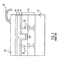
- Figure 1 shows a cross-section of a prior art array of image sensors.
- This array of image sensors includes PIN diode sensors located over a substrate 10.
- An interconnection structure 12 electrically connects an N-layer 14 of the PIN diodes to the substrate 10.
- An I-layer 16 is formed over the N-layer 14.
- a P-layer 18 is formed over the I-layer 16.
- the P-layer 18, the I-layer 16 and the N-layer 14 form the array of PIN diode sensors.
- a first conductive via 20 electrically connects a first diode sensor to the substrate 10, and a second conductive via 22 electrically connects a second diode sensor to the substrate 10.
- a transparent conductive layer 24 is located over the array of diode sensors.
- a conductive lead 26 is connected to the transparent conductive layer 24. The conductive lead 26 is connected to a bias voltage which allows biasing of the P-layer 18 of the array of PIN diode sensors to a selected voltage potential.
- a limitation of the image sensor structure of Figure 1 is the lack of shielding between the image sensors. Light received by a given sensor is also received by a neighboring sensor because there is no shielding of light between neighboring sensors. Light received by a given image sensor will also effect neighboring image sensors because current can flow through the N-layer 14 between neighboring image sensors. Charge can flow between the image sensors especially when the light intensity of the received light varies greatly between neighboring image sensors.
- the P-layer 18, the I-layer 16 and the N-layer 14 are shared by neighboring image sensors.
- a trench 28 is formed to provide some isolation between the image sensors by increasing the resistance between the N-layers sections of neighboring image sensors.
- the transparent conductive layer 24 must be electrically conductive to allow biasing of the PIN diodes, and must be transparent to allow the PIN diodes to receive light.
- the conductive lead 26 must be attached to the transparent conductive layer 24 with the aid of some type of clamp or support structure. The result being an electrical connection which is not reliable and which is expensive to produce.
- US 4,688,098 discloses that, in a solid state image sensor, first electrodes corresponding to pixels are arranged in a predetermined interval on a CCD structure.
- the first electrodes are electrically connected to storage sections of the CCD structure and electrically insulated from a transferring section of the CCD structure.
- Second electrodes are arranged in a predetermined interval on a flat surface of an insulating layer formed on the first electrodes and are electrically connected to the first electrodes.
- a photoconductive film for converting incident light rays to charges is formed on the second electrodes.
- a third electrode is formed on the photoconductive film through a barrier layer.
- Fourth electrodes which are electrically connected to the photoconductive film and electrically insulated from the second electrodes are buried in the insulating layer. An external voltage is applied to the fourth electrode.
- the active pixel sensor array include a conductive layer that provides a bias voltage to the array of active pixel sensors, and that is reliably electrically connected to a pixel sensor bias voltage which originates on the substrate.
- the present invention is an array of elevated active pixel sensors formed adjacent to a substrate that includes a conductive mesh that is reliably electrically connected to the pixel sensors and a pixel sensor bias voltage which is located on the substrate.
- the conductive mesh provides shielding of light received by each pixel sensor from the other pixel sensors. That is, the conductive mesh provides isolation between the active pixel sensors which reduces the effect that light received by an active pixel sensor of the array has on the other active pixel sensors of the array.
- the conductive mesh provides a bias voltage to the array of active pixel sensors.
- the substrate can be a CMOS substrate which includes image processing circuitry.
- the invention includes an array of active pixel sensors.
- the array of active pixel sensors includes a substrate.
- An interconnect structure is formed adjacent to the substrate.
- the interconnect structure includes a plurality of conductive vias.
- a plurality of photo sensors are formed adjacent to the interconnect structure.
- Each photo sensor includes a pixel electrode.
- Each pixel electrode is electrically connected to the substrate through a corresponding conductive via.
- An I-layer is formed over each of the pixel electrodes.
- the array of active pixel sensors further includes a conductive mesh formed adjacent to the photo sensors. An inner surface of the conductive mesh is electrically and physically connected to the photo sensors, and electrically connected to the substrate through a conductive via.
- a conductive mesh provides light shielding between photo sensors thereby reducing cross-talk between the photo sensors.
- the conductive mesh includes apertures aligning with at least one of the pixel electrodes of the photo sensors.
- the invention may further include a P-layer formed between the I-layer and the conductive mesh.
- the inner surface of the conductive mesh is electrically connected to the P-layer and the interconnect structure.
- the invention is embodied in an array of elevated active pixel sensors formed adjacent to a substrate that includes a conductive mesh that is reliably electrically connected to the pixel sensors and a pixel sensor bias voltage which is located on the substrate.
- the conductive mesh provides shielding of light received each pixel sensor from the other pixel sensors. That is, the conductive mesh provides isolation between the active pixel sensors which reduces the effect that light received by an active pixel sensor of the array has on the other active pixel sensors of the array.
- the conductive mesh provides a bias voltage to the array of active pixel sensors.
- Figure 2 shows a first embodiment of the invention.
- This embodiment includes a substrate 200.
- the substrate 200 includes electronic circuitry.
- An interconnection structure 210 is formed adjacent to the substrate 200.
- Pixel electrodes 222, 224, 226 are formed adjacent to the interconnection structure 210.
- Each pixel sensor of an array of pixel sensors includes an individual pixel electrode 222, 224, 226.
- An I-layer 220 is formed adjacent to the pixel electrodes 222, 224, 226.
- a P-layer 230 is formed adjacent to the I-layer 220.
- a conductive mesh 240 is formed adjacent to the P-layer 230.
- a first pixel electrode 222 of a first pixel sensor is electrically connected to the substrate 200 through a first conductive via 214.
- a second pixel electrode 224 of a second pixel sensor is electrically connected to the substrate 200 through a second conductive via 216
- a third pixel electrode 226 of a third pixel sensor is electrically connected to the substrate 200 through a third conductive via 218.
- the conductive mesh 240 is electrically connected to the substrate 200 through a fourth conductive via 212.
- Figure 3 shows a top-view of an embodiment of the invention.
- the top-view more clearly depicts the physical characteristics of the conductive mesh 240.
- the conductive mesh 240 include apertures 310 which align with the pixel electrodes 222, 224, 226 of the pixel sensors.
- the conductive mesh 240 provides shielding of light between the pixel sensors.
- the apertures 310 within the conductive mesh 240 allow light to be received by pixel sensors which align with the apertures 310 while shielding the received light from other pixel sensors.
- the conductive mesh 240 is physically and electrically connected to the P-layer 230.
- the conductive mesh 240 is also electrically connected to the substrate 200 through the fourth conductive via.
- the conductive mesh 240 is driven to a bias voltage potential by electronic circuitry within the substrate 200. The bias voltage potential biases the pixel sensors.
- the pixel sensors conduct charge when the pixel sensors receive light.
- the substrate 200 generally includes sense circuitry and signal processing circuitry.
- the sense circuitry senses how much charge the pixel sensors have conducted.
- the amount of charge conducted represents the intensity of light received by the pixel sensors.
- the substrate 200 can be CMOS (complementary metal oxide silicon), BiCMOS or Bipolar.
- the substrate 200 can include various types of substrate technology including charged coupled devices.
- the interconnection structure 210 is a standard CMOS interconnection structure.
- the structure and methods of forming this interconnection structure 210 are well known in the field of electronic integrated circuit fabrication.
- the interconnection structure 210 can be a subtractive metal structure, or a single or dual damascene structure.
- the conductive vias 214, 216, 218 pass through the pixel interconnect structure 210 and electrically connect the pixel electrodes 222, 224, 226 to the substrate 200.
- the fourth conductive via 212 passes through the pixel interconnect structure 210 and provides a reliable electrical connection between the conductive mesh 240 and the substrate 200.
- the conductive vias 212, 214, 216, 218 are formed from tungsten. Tungsten is generally used during fabrication because tungsten can fill high aspect ratio holes. That is, tungsten can be used to form narrow and relatively long interconnections.
- the conductive vias 212, 214, 216, 218 are formed using a chemical vapor deposition (CVD) process. Other materials which can be used to form the conductive vias 212, 214, 216, 218 include copper, aluminum or any other electrically conductive material.
- the pixel electrodes 222, 224, 226 are generally formed from a doped semiconductor.
- the doped semiconductor can be an N-layer of amorphous silicon.
- the pixel electrodes 222, 224, 226 must be thick enough, and doped heavily enough that the pixel electrodes 222, 224, 226 do not fully deplete when biased during operation.
- the pixel electrodes 222, 224, 226 are typically doped with phosphorous.
- the pixel electrodes 222, 224, 226 are typically deposited using plasma etched chemical vapor deposition (PECVD).
- PECVD is performed with a phosphorous containing gas.
- the phosphorous gas can be PH3.
- a silicon containing gas is included when forming amorphous silicon pixel electrodes.
- N-layer of amorphous silicon is typically used when forming the pixel electrodes 222, 224, 226 of the PIN diode active pixel sensors.
- the diode active pixel sensors can include an NIP sensor configuration.
- the pixel electrodes 222, 224, 226 are formed from a P-layer, and the P-layer 230 of Figure 2 is replaced with an N-layer.
- the I-layer 220 is generally formed from a hydrogenated amorphous silicon.
- the I-layer 220 can be deposited using a PECVD or a reactive sputtering process.
- the PECVD process must include a silicon containing gas.
- the deposition should be at a low enough temperature that hydrogen is retained within the film.
- the I-layer 220 is approximately one micron thick.
- the P-layer 230 is generally formed from amorphous silicon. Typically, the P-layer 230 is doped with Boron.
- the P-layer 230 can be deposited using PECVD. The PECVD is performed with a Boron containing gas. The Boron containing gas can be B2H6. A silicon containing gas is included when forming an amorphous silicon P-layer 230.
- the P-layer 230 thickness must generally be controlled to ensure that the P-layer 230 does not absorb too much short wavelength (blue) light.
- Another embodiment of the invention does not include a P-layer 230.
- the P-layer 230 can be eliminated with proper selection of the composition of the material within the conductive mesh 240, and proper selection of the doping levels of the pixel electrodes 222, 224, 226.
- the conductive mesh 240 provides a conductive connection between a top surface of the I-layer 220 of the pixel sensors and the interconnection structure 210.
- the pixel electrodes 222, 224, 226, the I-layer 220 and the P-layer 230 are generally formed from amorphous silicon.
- the pixel electrodes 222, 224, 226, the I-layer 220 and the P-layer 230 can also be formed from amorphous carbon, amorphous silicon carbide, amorphous germanium, or amorphous silicon-germanium. It should be understood that this list is not exhaustive.
- the conductive mesh 240 provides a conductive connection between the P-layer 230 and the interconnection structure 210. Light must pass through the apertures 310 of the conductive mesh 240 and is received by the pixel sensors.
- the conductive mesh 240 is formed from an opaque conductive material. Materials that can be used to form the conductive mesh 240 include aluminum, tungsten or copper. It is to be understood that this list is not exhaustive.
- the conductive mesh 240 can be formed by depositing the conductive mesh material 240 by a sputtering process, and then etching the conductive mesh material according to a mesh pattern to form the conductive mesh 240. Deposition through sputtering and etching according to a pattern are well known in the art of integrated circuit fabrication.
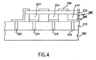
- FIG. 4 shows another embodiment of the invention.
- This embodiment includes I-layer sections 410 rather than a single I-layer 220. That is, each pixel sensor includes a separate I-layer section 410 rather than a single I-layer 220 which is formed as a part of many pixel sensors. Like the pixel electrodes 212, 214, 216, the I-layer sections can be etched according to a predetermined pattern.
- Figures 5-9 show processing steps which can be used to fabricate the embodiments shown in Figure 2, Figure 3 and Figure 4 .
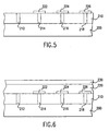
- Figure 5 shows a substrate 200 with an interconnection structure 210 formed over the substrate 200.
- Pixel electrodes 222, 224, 226 are formed over the interconnection structure 210.
- the structure and methods of forming this interconnection structure 210 are well known in the field of electronic integrated circuit fabrication.
- the interconnection structure 210 can be a subtractive metal structure, or a single or dual damascene structure.
- the interconnection structure 210 includes conductive vias 212, 214, 216, 218 that are generally formed from tungsten. Tungsten is generally used because during fabrication, tungsten can fill high aspect ratio holes. That is, tungsten can be used to form narrow and relatively long interconnections.
- the conductive vias 212, 214, 216, 218 are formed using a chemical vapor deposition (CVD) process.
- CVD chemical vapor deposition
- Other materials which can be used to form the conductive vias 212, 214, 216, 218 include copper, aluminum or any other electrically conductive material.
- the pixel electrodes 222, 224, 226 are deposited on the interconnection structure 210.
- a pixel electrode layer is first deposited over the interconnection structure 210. Then the pixel electrode layer is etched according to a predetermined pattern forming the pixel electrodes 222, 224, 226.
- An individual pixel electrode 222, 224, 226 is formed for each pixel sensor.
- the pixel electrodes 222, 224, 226 can be implemented with N-layer sections. Alternatively, the pixel electrodes 222, 224, 226 can be implemented with a conductive nitride, like, titanium nitride.
- the pixel electrodes 222, 224, 226 are typically deposited using PECVD.
- the PECVD is performed with a phosphorous containing gas.
- the phosphorous containing gas can be PH3.
- a silicon containing gas, such as Si2H6 or SiH4 is included when forming amorphous silicon pixel electrodes.
- the predetermined pixel electrode pattern is formed through a wet or dry etch of the deposited pixel electrode material.
- FIG. 6 shows an I-layer 220 and a P-layer 230 deposited over the plurality of pixel electrodes 222, 224, 226.
- the I-layer 220 is generally deposited using a PECVD or reactive sputtering process.
- the PECVD must include a silicon containing gas. The deposition should be at a low enough temperature that hydrogen is retained within the film.
- the P-layer 230 can also be deposited using PECVD.
- the PECVD is performed with a Boron containing gas.
- the Boron containing gas can be B2H6.
- a silicon containing gas is included when forming an amorphous silicon P-layer 230.
- Figure 7 shows the P-layer 230 and the I-layer 220 having been etched to provide access to the fourth conductive via 212.
- the fourth conductive via 212 is electrically connected to a reference voltage on the substrate 200 which is used to bias the array of pixel sensors.
- Figure 8 shows a conductive layer 810 deposited over the P-layer 230 which provides an electrical connection between the P-layer 230 and the fourth conductive via 212.
- the conductive layer 810 is formed from an opaque conductive material. Materials that can be used to form the conductive layer 810 include aluminum, tungsten or copper. It is to be understood that this list is not exhaustive.
- the conductive layer 810 is generally deposited through reactive sputtering. However, the conductive layer 810 can also be grown by evaporation, or deposited through chemical vapor deposition or plasma vapor deposition.
- Figure 9 shows the conductive layer 810 having been etched according to a predetermined pattern forming the conductive mesh 240. Etching of conductive materials is well known in the art of semiconductor processing.
Landscapes
- Solid State Image Pick-Up Elements (AREA)
- Light Receiving Elements (AREA)
- Electrodes Of Semiconductors (AREA)
Description
- This invention relates generally to photo diode active pixel sensors. In particular, it relates to a conductive mesh bias connection for an array of elevated active pixel sensors which provides light shielding between the active pixel sensors.
- An array of image sensors or light sensitive sensors detect the intensity of light received by the image sensors. The image sensors typically generate electronic signals that have amplitudes that are proportionate to the intensity of the light received by the image sensors. The image sensors can convert an optical image into a set of electronic signals. The electronic signals may represent intensities of colors of light received by the image sensors. The electronic signals can be conditioned and sampled to allow image processing.
- Integration of the image sensors with signal processing circuitry is becoming more important because integration enables miniaturization and simplification of imaging systems. Integration of image sensors along with analog and digital signal processing circuitry allows electronic imaging systems to be low cost, compact and require low power consumption.
- Historically, image sensors have predominantly been charged coupled devices (CCDs). CCDs are relatively small and can provide a high-fill factor. However, CCDs are very difficult to integrate with digital and analog circuitry. Further, CCDs dissipate large amounts of power and suffer from image smearing problems.
- An alternative to CCD sensors are active pixel sensors. Active pixel sensors can be fabricated using standard CMOS processes. Therefore, active pixel sensors can easily be integrated with digital and analog signal processing circuitry. Further, CMOS circuits dissipate small amounts of power.
-
Figure 1 shows a cross-section of a prior art array of image sensors. This array of image sensors includes PIN diode sensors located over asubstrate 10. Aninterconnection structure 12 electrically connects an N-layer 14 of the PIN diodes to thesubstrate 10. An I-layer 16 is formed over the N-layer 14. A P-layer 18 is formed over the I-layer 16. The P-layer 18, the I-layer 16 and the N-layer 14 form the array of PIN diode sensors. A first conductive via 20 electrically connects a first diode sensor to thesubstrate 10, and a second conductive via 22 electrically connects a second diode sensor to thesubstrate 10. A transparentconductive layer 24 is located over the array of diode sensors. Aconductive lead 26 is connected to the transparentconductive layer 24. Theconductive lead 26 is connected to a bias voltage which allows biasing of the P-layer 18 of the array of PIN diode sensors to a selected voltage potential. - A limitation of the image sensor structure of
Figure 1 is the lack of shielding between the image sensors. Light received by a given sensor is also received by a neighboring sensor because there is no shielding of light between neighboring sensors. Light received by a given image sensor will also effect neighboring image sensors because current can flow through the N-layer 14 between neighboring image sensors. Charge can flow between the image sensors especially when the light intensity of the received light varies greatly between neighboring image sensors. The P-layer 18, the I-layer 16 and the N-layer 14 are shared by neighboring image sensors. A trench 28 is formed to provide some isolation between the image sensors by increasing the resistance between the N-layers sections of neighboring image sensors. - Another limitation of the image sensor structure of
Figure 1 is the electrical connection between theconductive lead 26 and the transparentconductive layer 24. The transparentconductive layer 24 must be electrically conductive to allow biasing of the PIN diodes, and must be transparent to allow the PIN diodes to receive light. Generally, it is very difficult to bond to the types of materials that must be used to form the transparentconductive layer 24. Therefore, theconductive lead 26 must be attached to the transparentconductive layer 24 with the aid of some type of clamp or support structure. The result being an electrical connection which is not reliable and which is expensive to produce. -
US 4,688,098 discloses that, in a solid state image sensor, first electrodes corresponding to pixels are arranged in a predetermined interval on a CCD structure. The first electrodes are electrically connected to storage sections of the CCD structure and electrically insulated from a transferring section of the CCD structure. Second electrodes are arranged in a predetermined interval on a flat surface of an insulating layer formed on the first electrodes and are electrically connected to the first electrodes. A photoconductive film for converting incident light rays to charges is formed on the second electrodes. A third electrode is formed on the photoconductive film through a barrier layer. Fourth electrodes which are electrically connected to the photoconductive film and electrically insulated from the second electrodes are buried in the insulating layer. An external voltage is applied to the fourth electrode. - It is desirable to have an array of active pixel sensors formed adjacent to a substrate in which light received by an active pixel sensors of the array is shielded from the other active pixel sensors of the array. That is, it is desirable that isolation exist between the active pixel sensors which reduces the effect that light received by an active pixel sensor of the array has on the other active pixel sensors of the array. It is also desirable that the active pixel sensor array include a conductive layer that provides a bias voltage to the array of active pixel sensors, and that is reliably electrically connected to a pixel sensor bias voltage which originates on the substrate.
- It is an object of the invention to provide an improved array of active pixel sensors. This object may be achieved by an array of active pixel sensors according to the independent claim.
- The present invention is an array of elevated active pixel sensors formed adjacent to a substrate that includes a conductive mesh that is reliably electrically connected to the pixel sensors and a pixel sensor bias voltage which is located on the substrate. The conductive mesh provides shielding of light received by each pixel sensor from the other pixel sensors. That is, the conductive mesh provides isolation between the active pixel sensors which reduces the effect that light received by an active pixel sensor of the array has on the other active pixel sensors of the array. The conductive mesh provides a bias voltage to the array of active pixel sensors. The substrate can be a CMOS substrate which includes image processing circuitry.
- The invention includes an array of active pixel sensors. The array of active pixel sensors includes a substrate. An interconnect structure is formed adjacent to the substrate. The interconnect structure includes a plurality of conductive vias. A plurality of photo sensors are formed adjacent to the interconnect structure. Each photo sensor includes a pixel electrode. Each pixel electrode is electrically connected to the substrate through a corresponding conductive via. An I-layer is formed over each of the pixel electrodes. The array of active pixel sensors further includes a conductive mesh formed adjacent to the photo sensors. An inner surface of the conductive mesh is electrically and physically connected to the photo sensors, and electrically connected to the substrate through a conductive via.
- A conductive mesh provides light shielding between photo sensors thereby reducing cross-talk between the photo sensors.
- The conductive mesh includes apertures aligning with at least one of the pixel electrodes of the photo sensors.
- The invention may further include a P-layer formed between the I-layer and the conductive mesh. The inner surface of the conductive mesh is electrically connected to the P-layer and the interconnect structure.
- Other aspects and advantages of the present invention will become apparent from the following detailed description, taken in conjunction with the accompanying drawings, illustrating by way of example the principles of the invention.
-
-
Figure 1 shows a cross-section of a prior art array of image sensors. -
Figure 2 shows an embodiment of the invention. -
Figure 3 shows a top view of an embodiment of the invention. -
Figure 4 shows another embodiment of the invention. -
Figure 5 shows pixel electrodes deposited on the pixel interconnect structure. -
Figure 6 shows an I-layer and a P-layer deposited over a plurality of pixel electrodes. -
Figure 7 shows the P-layer and the I-layer selectively etched to allow access to a conductive via. -
Figure 8 shows a conductive layer deposited over the P-layer which provides an electrical connection between the P-layer and the interconnection structure. -
Figure 9 shows the transparent conductive layer having been etched according to a predetermined pattern. - As shown in the drawings for purposes of illustration, the invention is embodied in an array of elevated active pixel sensors formed adjacent to a substrate that includes a conductive mesh that is reliably electrically connected to the pixel sensors and a pixel sensor bias voltage which is located on the substrate. The conductive mesh provides shielding of light received each pixel sensor from the other pixel sensors. That is, the conductive mesh provides isolation between the active pixel sensors which reduces the effect that light received by an active pixel sensor of the array has on the other active pixel sensors of the array. The conductive mesh provides a bias voltage to the array of active pixel sensors.
-
Figure 2 shows a first embodiment of the invention. This embodiment includes asubstrate 200. Thesubstrate 200 includes electronic circuitry. Aninterconnection structure 210 is formed adjacent to thesubstrate 200.Pixel electrodes interconnection structure 210. Each pixel sensor of an array of pixel sensors includes anindividual pixel electrode layer 220 is formed adjacent to thepixel electrodes layer 230 is formed adjacent to the I-layer 220. Aconductive mesh 240 is formed adjacent to the P-layer 230. Afirst pixel electrode 222 of a first pixel sensor is electrically connected to thesubstrate 200 through a first conductive via 214. Asecond pixel electrode 224 of a second pixel sensor is electrically connected to thesubstrate 200 through a second conductive via 216, Athird pixel electrode 226 of a third pixel sensor is electrically connected to thesubstrate 200 through a third conductive via 218. Theconductive mesh 240 is electrically connected to thesubstrate 200 through a fourth conductive via 212. -
Figure 3 shows a top-view of an embodiment of the invention. The top-view more clearly depicts the physical characteristics of theconductive mesh 240. Theconductive mesh 240 includeapertures 310 which align with thepixel electrodes conductive mesh 240 provides shielding of light between the pixel sensors. Theapertures 310 within theconductive mesh 240 allow light to be received by pixel sensors which align with theapertures 310 while shielding the received light from other pixel sensors. - The
conductive mesh 240 is physically and electrically connected to the P-layer 230. Theconductive mesh 240 is also electrically connected to thesubstrate 200 through the fourth conductive via. Theconductive mesh 240 is driven to a bias voltage potential by electronic circuitry within thesubstrate 200. The bias voltage potential biases the pixel sensors. - The pixel sensors conduct charge when the pixel sensors receive light. The
substrate 200 generally includes sense circuitry and signal processing circuitry. The sense circuitry senses how much charge the pixel sensors have conducted. The amount of charge conducted represents the intensity of light received by the pixel sensors. Generally, thesubstrate 200 can be CMOS (complementary metal oxide silicon), BiCMOS or Bipolar. Thesubstrate 200 can include various types of substrate technology including charged coupled devices. - Typically, the
interconnection structure 210 is a standard CMOS interconnection structure. The structure and methods of forming thisinterconnection structure 210 are well known in the field of electronic integrated circuit fabrication. Theinterconnection structure 210 can be a subtractive metal structure, or a single or dual damascene structure. - The
conductive vias pixel interconnect structure 210 and electrically connect thepixel electrodes substrate 200. The fourth conductive via 212 passes through thepixel interconnect structure 210 and provides a reliable electrical connection between theconductive mesh 240 and thesubstrate 200. Typically, theconductive vias conductive vias conductive vias - The
pixel electrodes pixel electrodes pixel electrodes pixel electrodes - The
pixel electrodes - An N-layer of amorphous silicon is typically used when forming the
pixel electrodes pixel electrodes layer 230 ofFigure 2 is replaced with an N-layer. - The I-
layer 220 is generally formed from a hydrogenated amorphous silicon. The I-layer 220 can be deposited using a PECVD or a reactive sputtering process. The PECVD process must include a silicon containing gas. The deposition should be at a low enough temperature that hydrogen is retained within the film. The I-layer 220 is approximately one micron thick. - The P-
layer 230 is generally formed from amorphous silicon. Typically, the P-layer 230 is doped with Boron. The P-layer 230 can be deposited using PECVD. The PECVD is performed with a Boron containing gas. The Boron containing gas can be B2H6. A silicon containing gas is included when forming an amorphous silicon P-layer 230. The P-layer 230 thickness must generally be controlled to ensure that the P-layer 230 does not absorb too much short wavelength (blue) light. - Another embodiment of the invention does not include a P-
layer 230. The P-layer 230 can be eliminated with proper selection of the composition of the material within theconductive mesh 240, and proper selection of the doping levels of thepixel electrodes conductive mesh 240 provides a conductive connection between a top surface of the I-layer 220 of the pixel sensors and theinterconnection structure 210. - As previously described, the
pixel electrodes layer 220 and the P-layer 230 are generally formed from amorphous silicon. However, thepixel electrodes layer 220 and the P-layer 230 can also be formed from amorphous carbon, amorphous silicon carbide, amorphous germanium, or amorphous silicon-germanium. It should be understood that this list is not exhaustive. - The
conductive mesh 240 provides a conductive connection between the P-layer 230 and theinterconnection structure 210. Light must pass through theapertures 310 of theconductive mesh 240 and is received by the pixel sensors. Theconductive mesh 240 is formed from an opaque conductive material. Materials that can be used to form theconductive mesh 240 include aluminum, tungsten or copper. It is to be understood that this list is not exhaustive. - The
conductive mesh 240 can be formed by depositing theconductive mesh material 240 by a sputtering process, and then etching the conductive mesh material according to a mesh pattern to form theconductive mesh 240. Deposition through sputtering and etching according to a pattern are well known in the art of integrated circuit fabrication. -
Figure 4 shows another embodiment of the invention. This embodiment includes I-layer sections 410 rather than a single I-layer 220. That is, each pixel sensor includes a separate I-layer section 410 rather than a single I-layer 220 which is formed as a part of many pixel sensors. Like thepixel electrodes -
Figures 5-9 show processing steps which can be used to fabricate the embodiments shown inFigure 2, Figure 3 andFigure 4 . -
Figure 5 shows asubstrate 200 with aninterconnection structure 210 formed over thesubstrate 200.Pixel electrodes interconnection structure 210. The structure and methods of forming thisinterconnection structure 210 are well known in the field of electronic integrated circuit fabrication. Theinterconnection structure 210 can be a subtractive metal structure, or a single or dual damascene structure. - The
interconnection structure 210 includesconductive vias conductive vias conductive vias - The
pixel electrodes interconnection structure 210. A pixel electrode layer is first deposited over theinterconnection structure 210. Then the pixel electrode layer is etched according to a predetermined pattern forming thepixel electrodes individual pixel electrode pixel electrodes pixel electrodes - The
pixel electrodes -
Figure 6 shows an I-layer 220 and a P-layer 230 deposited over the plurality ofpixel electrodes layer 220 is generally deposited using a PECVD or reactive sputtering process. The PECVD must include a silicon containing gas. The deposition should be at a low enough temperature that hydrogen is retained within the film. The P-layer 230 can also be deposited using PECVD. The PECVD is performed with a Boron containing gas. The Boron containing gas can be B2H6. A silicon containing gas is included when forming an amorphous silicon P-layer 230. -
Figure 7 shows the P-layer 230 and the I-layer 220 having been etched to provide access to the fourth conductive via 212. The fourth conductive via 212 is electrically connected to a reference voltage on thesubstrate 200 which is used to bias the array of pixel sensors. -
Figure 8 shows aconductive layer 810 deposited over the P-layer 230 which provides an electrical connection between the P-layer 230 and the fourth conductive via 212. Theconductive layer 810 is formed from an opaque conductive material. Materials that can be used to form theconductive layer 810 include aluminum, tungsten or copper. It is to be understood that this list is not exhaustive. - The
conductive layer 810 is generally deposited through reactive sputtering. However, theconductive layer 810 can also be grown by evaporation, or deposited through chemical vapor deposition or plasma vapor deposition. -
Figure 9 shows theconductive layer 810 having been etched according to a predetermined pattern forming theconductive mesh 240. Etching of conductive materials is well known in the art of semiconductor processing. - Although specific embodiments of the invention have been described and illustrated, the invention is not to be limited to the specific forms or arrangements of parts so described and illustrated. The invention is limited only by the claims.
Claims (9)
- An array of active pixel sensors comprising:a substrate (200) comprising an electronic circuit;an interconnect structure (210) over the substrate, the interconnect structure comprising a plurality of conductive vias;a plurality of photo sensors over the interconnect structure, each photo sensor comprising:wherein the conductive mesh (240) comprises apertures aligned with the pixel electrodes of the photo sensors.a pixel electrode (222, 224, 226), the pixel electrode electrically connected to the substrate through a corresponding conductive via (214, 216, 218);an I-layer (220) formed over the pixel electrode;the array of active pixel sensors further comprising a common top electrode for biasing the photo sensors, characterized in that
the common top electrode includes a light shielding conductive mesh (240) formed over the photo sensors, an inner surface of the conductive mesh electrically and physically connected to the photo sensors, and electrically connected to the substrate through a conductive via (212), - The active pixel sensor as recited in claim 1, wherein each pixel electrode (222, 224, 226) comprises an N-layer.
- The active pixel sensor as recited in claim 1, wherein the I-layer (220) and the pixel electrodes (222, 224, 226) each comprise amorphous silicon.
- The active pixel sensor as recited in claim 1, further comprising a P-layer (230) formed between the I-layer (220) and the conductive mesh (240), the inner surface of the conductive mesh physically and electrically connected to the P-layer and electrically connected to the substrate through a conductive via.
- The active pixel sensor as recited in claim 4, wherein the P-layer (230) comprises amorphous silicon.
- The active pixel sensor as recited in claim 1, wherein the inner surface of the conductive mesh (240) is electrically connected to the substrate through at least one tungsten conductive via (212).
- The active pixel sensor as recited in claim 1, wherein the substrate (200) is selected from a group including CMOS, active circuits which sense charge accumulated by the photo sensors due to the photo sensors receiving light, and charge coupled devices.
- The active pixel sensor as recited in claim 1, wherein each pixel electrode (222, 224, 226) comprises a P-layer.
- The active pixel sensor as recited in claim 1, wherein each pixel electrode (222, 224, 226) comprises a conductive metal.
Applications Claiming Priority (2)
| Application Number | Priority Date | Filing Date | Title |
|---|---|---|---|
| US496941 | 2000-02-03 | ||
| US09/496,941 US6396118B1 (en) | 2000-02-03 | 2000-02-03 | Conductive mesh bias connection for an array of elevated active pixel sensors |
Publications (3)
| Publication Number | Publication Date |
|---|---|
| EP1122790A2 EP1122790A2 (en) | 2001-08-08 |
| EP1122790A3 EP1122790A3 (en) | 2003-12-03 |
| EP1122790B1 true EP1122790B1 (en) | 2008-08-27 |
Family
ID=23974822
Family Applications (1)
| Application Number | Title | Priority Date | Filing Date |
|---|---|---|---|
| EP00122087A Expired - Lifetime EP1122790B1 (en) | 2000-02-03 | 2000-10-11 | A conductive mesh bias connection for an array of elevated active pixel sensors |
Country Status (4)
| Country | Link |
|---|---|
| US (1) | US6396118B1 (en) |
| EP (1) | EP1122790B1 (en) |
| JP (1) | JP2001257336A (en) |
| DE (1) | DE60040055D1 (en) |
Families Citing this family (18)
| Publication number | Priority date | Publication date | Assignee | Title |
|---|---|---|---|---|
| US20040113220A1 (en) * | 2000-12-21 | 2004-06-17 | Peter Rieve | Optoelectronic component for conversion electromagnetic radiation into an intensity-dependent photocurrent |
| US6909150B2 (en) * | 2001-07-23 | 2005-06-21 | Agere Systems Inc. | Mixed signal integrated circuit with improved isolation |
| FR2844098B1 (en) * | 2002-09-03 | 2004-11-19 | Atmel Grenoble Sa | OPTICAL MICROSYSTEM AND MANUFACTURING METHOD |
| FR2848027B1 (en) * | 2002-11-29 | 2006-02-10 | Commissariat Energie Atomique | PHOTOELECTRIC DETECTION DEVICE AND METHOD FOR PRODUCING THE SAME |
| FR2852147B1 (en) | 2003-03-06 | 2005-09-30 | Commissariat Energie Atomique | PIXEL MATRIX DETECTORS INTEGRATED ON LOAD READING CIRCUIT |
| US20050007473A1 (en) * | 2003-07-08 | 2005-01-13 | Theil Jeremy A. | Reducing image sensor lag |
| ES2246109B2 (en) * | 2003-09-08 | 2007-05-16 | Univ Madrid Politecnica | MULTI-RESOLUTION SCANNER SYSTEM FOR THE EXPLORATION OF MICROMATRICES. |
| FR2907261B1 (en) * | 2006-10-12 | 2009-01-30 | Commissariat Energie Atomique | DEVICE FOR ELECTROMAGNETIC COUPLING OF AN ELECTROMAGNETIC RADIATION DETECTOR |
| US8263924B2 (en) * | 2007-01-17 | 2012-09-11 | Forza Silicon | Ground and power mesh in an integrated circuit chip |
| KR100997299B1 (en) * | 2007-09-07 | 2010-11-29 | 주식회사 동부하이텍 | Image sensor and manufacturing method |
| DE102008046030A1 (en) * | 2007-09-07 | 2009-06-10 | Dongbu Hitek Co., Ltd. | Image sensor and method for its production |
| KR100922935B1 (en) * | 2007-11-05 | 2009-10-22 | 주식회사 동부하이텍 | Image sensor and manufacturing method |
| KR20100078145A (en) * | 2008-12-30 | 2010-07-08 | 주식회사 동부하이텍 | Image sensor and method for manufacturing thereof |
| WO2011148574A1 (en) * | 2010-05-28 | 2011-12-01 | パナソニック株式会社 | Solid-state image pickup device |
| US8482090B2 (en) | 2010-07-15 | 2013-07-09 | Exelis, Inc. | Charged particle collector for a CMOS imager |
| US8753917B2 (en) * | 2010-12-14 | 2014-06-17 | International Business Machines Corporation | Method of fabricating photoconductor-on-active pixel device |
| EP3322342B1 (en) * | 2015-07-14 | 2023-11-22 | DOSE Smart Imaging | Apparatus for radiation detection in a digital imaging system |
| US11616093B2 (en) | 2017-12-28 | 2023-03-28 | Sony Semiconductor Solutions Corporation | Light receiving element and electronic apparatus |
Family Cites Families (14)
| Publication number | Priority date | Publication date | Assignee | Title |
|---|---|---|---|---|
| JPS6040232B2 (en) * | 1980-04-15 | 1985-09-10 | 松下電器産業株式会社 | solid-state imaging device |
| US4745451A (en) * | 1983-07-01 | 1988-05-17 | Rca Corporation | Photodetector array and a method of making same |
| EP0186162B1 (en) * | 1984-12-24 | 1989-05-31 | Kabushiki Kaisha Toshiba | Solid state image sensor |
| US5076670A (en) * | 1989-10-13 | 1991-12-31 | Hughes Aircraft Company | Isolated pixel liquid crystal light valve structure |
| US5182624A (en) * | 1990-08-08 | 1993-01-26 | Minnesota Mining And Manufacturing Company | Solid state electromagnetic radiation detector fet array |
| JPH04216670A (en) * | 1990-12-17 | 1992-08-06 | Canon Inc | Photoelectric transducer |
| JPH04280677A (en) * | 1991-03-08 | 1992-10-06 | Sony Corp | Laminated type solid-state image pickup device |
| US5578837A (en) * | 1995-01-03 | 1996-11-26 | Xerox Corporation | Integrating hyperacuity sensors and arrays thereof |
| US5936230A (en) * | 1996-11-19 | 1999-08-10 | Xerox Corporation | High light collection X-ray image sensor array |
| US6069365A (en) * | 1997-11-25 | 2000-05-30 | Alan Y. Chow | Optical processor based imaging system |
| US6018187A (en) * | 1998-10-19 | 2000-01-25 | Hewlett-Packard Cmpany | Elevated pin diode active pixel sensor including a unique interconnection structure |
| US5936261A (en) * | 1998-11-18 | 1999-08-10 | Hewlett-Packard Company | Elevated image sensor array which includes isolation between the image sensors and a unique interconnection |
| US6215164B1 (en) * | 1999-07-26 | 2001-04-10 | Agilent Technologies, Inc. | Elevated image sensor array which includes isolation between uniquely shaped image sensors |
| US6229191B1 (en) * | 1999-11-19 | 2001-05-08 | Agilent Technologies, Inc. | Conductive guard rings for elevated active pixel sensors |
-
2000
- 2000-02-03 US US09/496,941 patent/US6396118B1/en not_active Expired - Lifetime
- 2000-10-11 EP EP00122087A patent/EP1122790B1/en not_active Expired - Lifetime
- 2000-10-11 DE DE60040055T patent/DE60040055D1/en not_active Expired - Lifetime
-
2001
- 2001-02-05 JP JP2001027942A patent/JP2001257336A/en active Pending
Also Published As
| Publication number | Publication date |
|---|---|
| DE60040055D1 (en) | 2008-10-09 |
| US6396118B1 (en) | 2002-05-28 |
| EP1122790A2 (en) | 2001-08-08 |
| EP1122790A3 (en) | 2003-12-03 |
| JP2001257336A (en) | 2001-09-21 |
Similar Documents
| Publication | Publication Date | Title |
|---|---|---|
| US6018187A (en) | Elevated pin diode active pixel sensor including a unique interconnection structure | |
| US5936261A (en) | Elevated image sensor array which includes isolation between the image sensors and a unique interconnection | |
| EP1045450B1 (en) | Image sensor array device | |
| US6215164B1 (en) | Elevated image sensor array which includes isolation between uniquely shaped image sensors | |
| US6396118B1 (en) | Conductive mesh bias connection for an array of elevated active pixel sensors | |
| EP1102321B1 (en) | Conductive guard rings for active pixel sensors | |
| US6111300A (en) | Multiple color detection elevated pin photo diode active pixel sensor | |
| US6501065B1 (en) | Image sensor using a thin film photodiode above active CMOS circuitry | |
| US6114739A (en) | Elevated pin diode active pixel sensor which includes a patterned doped semiconductor electrode | |
| US6710370B2 (en) | Image sensor with performance enhancing structures | |
| US20040041932A1 (en) | Photoconductor-on-active-pixel (POAP) sensor utilizing a multi-layered radiation absorbing structure | |
| US6649993B2 (en) | Simplified upper electrode contact structure for PIN diode active pixel sensor | |
| US7812350B2 (en) | Image sensor and method for manufacturing the same | |
| KR100556511B1 (en) | Image sensor and its manufacture | |
| EP1344259B1 (en) | Optoelectronic component for conversion of electromagnetic radiation into an intensity-dependent photocurrent | |
| US6163030A (en) | MOS imaging device | |
| US7732813B2 (en) | Image sensor and method for manufacturing the same | |
| US20040041930A1 (en) | Photoconductor-on-active-pixel (POAP) sensor utilizing a multi-layered radiation absorbing structure | |
| US7825494B2 (en) | Image sensor and method for manufacturing the same | |
| US6384460B1 (en) | Self-aligned metal electrode structure for elevated sensors |
Legal Events
| Date | Code | Title | Description |
|---|---|---|---|
| PUAI | Public reference made under article 153(3) epc to a published international application that has entered the european phase |
Free format text: ORIGINAL CODE: 0009012 |
|
| AK | Designated contracting states |
Kind code of ref document: A2 Designated state(s): AT BE CH CY DE DK ES FI FR GB GR IE IT LI LU MC NL PT SE |
|
| AX | Request for extension of the european patent |
Free format text: AL;LT;LV;MK;RO;SI |
|
| RAP1 | Party data changed (applicant data changed or rights of an application transferred) |
Owner name: AGILENT TECHNOLOGIES, INC. (A DELAWARE CORPORATION |
|
| PUAL | Search report despatched |
Free format text: ORIGINAL CODE: 0009013 |
|
| AK | Designated contracting states |
Kind code of ref document: A3 Designated state(s): AT BE CH CY DE DK ES FI FR GB GR IE IT LI LU MC NL PT SE |
|
| AX | Request for extension of the european patent |
Extension state: AL LT LV MK RO SI |
|
| 17P | Request for examination filed |
Effective date: 20040217 |
|
| 17Q | First examination report despatched |
Effective date: 20040614 |
|
| AKX | Designation fees paid |
Designated state(s): DE FR GB |
|
| RAP1 | Party data changed (applicant data changed or rights of an application transferred) |
Owner name: AVAGO TECHNOLOGIES GENERAL IP (SINGAPORE) PTE. LTD |
|
| GRAP | Despatch of communication of intention to grant a patent |
Free format text: ORIGINAL CODE: EPIDOSNIGR1 |
|
| GRAS | Grant fee paid |
Free format text: ORIGINAL CODE: EPIDOSNIGR3 |
|
| GRAA | (expected) grant |
Free format text: ORIGINAL CODE: 0009210 |
|
| AK | Designated contracting states |
Kind code of ref document: B1 Designated state(s): DE FR GB |
|
| REG | Reference to a national code |
Ref country code: GB Ref legal event code: FG4D |
|
| REF | Corresponds to: |
Ref document number: 60040055 Country of ref document: DE Date of ref document: 20081009 Kind code of ref document: P |
|
| RAP2 | Party data changed (patent owner data changed or rights of a patent transferred) |
Owner name: MICRON TECHNOLOGY INC, A LEGAL ENTITY OF DELAWARE |
|
| PLBE | No opposition filed within time limit |
Free format text: ORIGINAL CODE: 0009261 |
|
| STAA | Information on the status of an ep patent application or granted ep patent |
Free format text: STATUS: NO OPPOSITION FILED WITHIN TIME LIMIT |
|
| 26N | No opposition filed |
Effective date: 20090528 |
|
| PGFP | Annual fee paid to national office [announced via postgrant information from national office to epo] |
Ref country code: FR Payment date: 20091029 Year of fee payment: 10 |
|
| REG | Reference to a national code |
Ref country code: GB Ref legal event code: 732E Free format text: REGISTERED BETWEEN 20101007 AND 20101013 |
|
| PG25 | Lapsed in a contracting state [announced via postgrant information from national office to epo] |
Ref country code: FR Free format text: LAPSE BECAUSE OF NON-PAYMENT OF DUE FEES Effective date: 20101102 |
|
| REG | Reference to a national code |
Ref country code: FR Ref legal event code: ST Effective date: 20110630 |
|
| PGFP | Annual fee paid to national office [announced via postgrant information from national office to epo] |
Ref country code: GB Payment date: 20190923 Year of fee payment: 20 |
|
| PGFP | Annual fee paid to national office [announced via postgrant information from national office to epo] |
Ref country code: DE Payment date: 20190918 Year of fee payment: 20 |
|
| REG | Reference to a national code |
Ref country code: DE Ref legal event code: R071 Ref document number: 60040055 Country of ref document: DE |
|
| REG | Reference to a national code |
Ref country code: GB Ref legal event code: PE20 Expiry date: 20201010 |
|
| PG25 | Lapsed in a contracting state [announced via postgrant information from national office to epo] |
Ref country code: GB Free format text: LAPSE BECAUSE OF EXPIRATION OF PROTECTION Effective date: 20201010 |