EP1119824B1 - Fingerprint image optical input apparatus - Google Patents
Fingerprint image optical input apparatus Download PDFInfo
- Publication number
- EP1119824B1 EP1119824B1 EP99947151A EP99947151A EP1119824B1 EP 1119824 B1 EP1119824 B1 EP 1119824B1 EP 99947151 A EP99947151 A EP 99947151A EP 99947151 A EP99947151 A EP 99947151A EP 1119824 B1 EP1119824 B1 EP 1119824B1
- Authority
- EP
- European Patent Office
- Prior art keywords
- platen
- fingerprint
- light
- sensor
- interior surface
- Prior art date
- Legal status (The legal status is an assumption and is not a legal conclusion. Google has not performed a legal analysis and makes no representation as to the accuracy of the status listed.)
- Expired - Lifetime
Links
Images


Classifications
-
- G—PHYSICS
- G06—COMPUTING; CALCULATING OR COUNTING
- G06V—IMAGE OR VIDEO RECOGNITION OR UNDERSTANDING
- G06V40/00—Recognition of biometric, human-related or animal-related patterns in image or video data
- G06V40/10—Human or animal bodies, e.g. vehicle occupants or pedestrians; Body parts, e.g. hands
- G06V40/12—Fingerprints or palmprints
- G06V40/13—Sensors therefor
- G06V40/1324—Sensors therefor by using geometrical optics, e.g. using prisms
-
- G—PHYSICS
- G06—COMPUTING; CALCULATING OR COUNTING
- G06F—ELECTRIC DIGITAL DATA PROCESSING
- G06F18/00—Pattern recognition
-
- G—PHYSICS
- G06—COMPUTING; CALCULATING OR COUNTING
- G06V—IMAGE OR VIDEO RECOGNITION OR UNDERSTANDING
- G06V40/00—Recognition of biometric, human-related or animal-related patterns in image or video data
- G06V40/10—Human or animal bodies, e.g. vehicle occupants or pedestrians; Body parts, e.g. hands
- G06V40/12—Fingerprints or palmprints
- G06V40/1335—Combining adjacent partial images (e.g. slices) to create a composite input or reference pattern; Tracking a sweeping finger movement
-
- A—HUMAN NECESSITIES
- A61—MEDICAL OR VETERINARY SCIENCE; HYGIENE
- A61B—DIAGNOSIS; SURGERY; IDENTIFICATION
- A61B5/00—Measuring for diagnostic purposes; Identification of persons
- A61B5/117—Identification of persons
- A61B5/1171—Identification of persons based on the shapes or appearances of their bodies or parts thereof
- A61B5/1172—Identification of persons based on the shapes or appearances of their bodies or parts thereof using fingerprinting
-
- H—ELECTRICITY
- H01—ELECTRIC ELEMENTS
- H01L—SEMICONDUCTOR DEVICES NOT COVERED BY CLASS H10
- H01L2224/00—Indexing scheme for arrangements for connecting or disconnecting semiconductor or solid-state bodies and methods related thereto as covered by H01L24/00
- H01L2224/01—Means for bonding being attached to, or being formed on, the surface to be connected, e.g. chip-to-package, die-attach, "first-level" interconnects; Manufacturing methods related thereto
- H01L2224/42—Wire connectors; Manufacturing methods related thereto
- H01L2224/47—Structure, shape, material or disposition of the wire connectors after the connecting process
- H01L2224/48—Structure, shape, material or disposition of the wire connectors after the connecting process of an individual wire connector
- H01L2224/4805—Shape
- H01L2224/4809—Loop shape
- H01L2224/48091—Arched
Definitions
- This invention relates to a method of creating electronic images of a finger or other object with ridges and the like, and a compact optical apparatus to project high contrast image slices of a fingerprint onto sensors.
- the prior art for fingerprint sensors is exemplified by United States Patent No. 4,784,484 ("the '484 patent") which issued 15 November 1988 for an invention called “Method and Apparatus for Automatic Scanning of Fingerprints.”
- the '484 patent uses a separate sensing means to measure the speed of finger motion.
- the '484 patent does not teach the use of FTIR to view a high contrast image of the fingerprint.
- the '484 patent does not employ a gradient index rod lens array or an array of relay lens pairs.
- the prior art for fingerprint sensors is also exemplified by United States Patent No. 5,619,586 (“the '586 patent”) which issued 8 April, 1997 for an invention called “Method and Apparatus for Producing a Directly Viewable Image of a Fingerprint.”
- the '586 patent shows prior art employing FTIR to obtain a high contrast fingerprint image.
- the '586 patent shows imaging of the entire fingerprint at once as an area image, instead of a narrow strip image projected onto a linear array sensor.
- the '586 patent does not show the use of gradient index rod lenses or relay lenses to image the fingerprint.
- the invention provides a fingerprint image optical input apparatus in the form of a contact image sensor (CIS) which projects high contrast image slices onto a linear array sensor.
- Novel optics are employed to provide a high contrast image by means of FTIR or direct illumination of ridges of the fingerprint which is projected by a GRIN (GRadient INdex of refraction) lens array onto a linear array sensor.
- GRIN GRadient INdex of refraction
- the generally preferred embodiment is a miniaturized CIS sensor arranged to view the width of the moving fingerprint as it is wiped over the optically transparent platen of the sensor.
- light must be introduced inside the platen.
- Light from the light source may be introduced inside the transparent platen through a flat or curved surface, which acts as a lens to direct the light and help collimate the light so that it forms a flat sheet of light the width of the linear array sensor.
- the light may optionally be directed inside the platen by using total internal reflection (TIR) or reflections from a mirrorlike surface or surfaces.
- TIR total internal reflection
- the use of reflections to direct the light inside the platen allows the light source to be located anywhere convenient, such as on a printed circuit board; the location of the light source can alter the form of the platen, or allow the platen to be made more compactly.
- the reflective surfaces or TIR surfaces of the platen can be slightly rough, not perfectly flat, to partially diffuse the light beam and thus cause more even lighting of the fingerprint.
- a high contrast image may be obtained by viewing the fingerprint through the transparent platen at an oblique angle; the fingerprint image is then focused by a GRIN lens array onto a linear sensor array.
- the GRIN lens or other focusing means can be arranged to view reflected images of the fingerprint, and to project reflected images onto the linear array sensor.
- To provide a high contrast image of the fingerprint light is directed at an angle to the top interior surface of the platen (typically 45 degrees or more to a line normal to the surface of the platen, depending on the index of refraction of the platen, which is advantageously greater than 1.5), where it is reflected by TIR if no fingerprint is present.
- a high contrast image may also be obtained by viewing the fingerprint through the transparent platen at an oblique angle, but with direct illumination of the finger by light directed substantially normal to the internal imaging surface of the platen.
- the fingerprint image is then focused by a GRIN lens array onto a linear sensor array.
- the GRIN lens or other focusing means can be arranged to view reflected images of the fingerprint, and to project reflected images onto the linear array sensor.
- the light escapes through the surface of the platen, while the GRIN lens sees a black surface by TIR from the platen.
- a high contrast image of the fingerprint is obtained by when a finger is placed on the platen and the fingerprint ridges are selectively illuminated due to physical contact with the surface of the platen.
- the fingerprint ridges touch the top surface of the platen, the fingerprint ridges glow with scattered light, resulting in a bright pattern for the fingerprint ridges and darker regions at the fingerprint valleys.
- the oblique viewing angle of the GRIN lens enhances contrast, while allowing limited viewing of fingerprint ridge details that are near to, but not touching, the platen.
- the angled surface of the platen has a raised strip to increase the pressure of the finger on the imaging surface, thereby giving better contact for total internal reflection.
- the platen surface or raised portion can also be constructed of silicone or some other material with optical wetting or low friction properties to improve imaging or finger movement respectively.
- a liquid reservoir can be integrated into the platen or an adjacent surface to allowing wetting of the finger with oil or other liquid to improve the total FTIR or fingerprint ridge glow imaging, as well as lubricating the finger for smooth motion.
- the platen itself can be part of the protective housing of the sensing elements. Surfaces of the platen can be coated in a light absorbing material to absorb stray light, thus reducing the noise at the sensor element.
- the high contrast fingerprint image is viewed by a GRIN lens array, or alternatively a relay lens pair array, or any other functionally equivalent means that creates a series of coherent overlapping images.
- the GRIN lens array looks at an oblique angle to the platen; the narrow fingerprint strip image is focused by the GRIN lens array onto the width of a linear array sensor, which may have one linear array of light sensing pixels or two or more parallel linear arrays of light sensing pixels.
- the CIS sensor for fingerprint imaging can be arranged in several novel configurations, which can be optimized for different applications and manufacturing techniques.
- the different features of various configurations may be utilized or combined, and other materials, components or technologies may used or combined to achieve substantially similar fingerprint imaging systems.
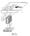
- FIG. 1A a basic CIS (Contact Image Sensor) is shown, which is commonly used in prior art facsimile machines and sheet-feed document scanners.
- a CIS imager is comprised of four basic components, which include a transparent platen, light source, lens array, and linear array sensor.
- the platen 1 is made of transparent glass or plastic, or other suitable transparent material.
- the light source 2 is conveniently an array of light emitting diodes (LEDs) or any other suitable source of light such as an electro-luminescent strip or miniature fluorescent tube.
- the lens system is typically a GRIN lens array 3, or it could be replaced by a relay lens array 6 as shown in Figure 1B.
- the linear array optical sensor 4, with a single linear array, or two or more parallel rows of light sensing pixels, may use CCD (charge coupled device) pixels, or may use CMOS (complementary metal oxide semiconductor) APS (active pixel sensing) pixels, photo-diode pixels, or any other linear array of light sensing or infrared sensing pixel technology.
- the width of platen 1, light source 2, GRIN lens array 3 and linear array sensor 4 may be any convenient length, suited to the imaging task at hand.
- the CIS sensor is shown imaging a printed sheet of paper 5 which is moved across the platen 1.
- paper 5 is mechanically moved across the platen; alternatively, the CIS sensor may be mechanically moved beneath paper 5 on a fixed platen.
- light source 2 shines light beam 2a through transparent platen 1 and illuminates the object, such as printed letters on paper 5. Some light 2b is then scattered and reflected from paper 5 and is viewed by GRIN lens array 3 and focused as light 2c onto linear array sensor 4.
- An electronic gray scale image is gathered line by line by the linear array sensor 4, and is subsequently stored, altered, processed, interpreted, transmitted, displayed, printed or otherwise used.
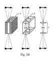
- FIG. 1B compares GRIN lens array 3 with relay lens array 6, which is comprised of a linear array of relay lens pairs.
- relay lens array 6 is the functional equivalent of GRIN lens array 3, which is a 1:1 imager (no magnification, de-magnification or image inversion).
- the GRIN lens array 3 and relay lens array 6 both create a series of overlapping coherent images to create a single narrow image the width of the array.
- the general optical properties of a relay lens is shown schematically with relay lens pair 7, whereby an image is transmitted, or relayed, to the focal plane without change in size or orientation.
- GRIN lens array 3 utilizes optical fibers as rod lenses to refract the image, to achieve the same optical result.
- a suitably designed relay lens array may be substituted for a GRIN lens array.
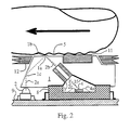
- FIG 2 a general embodiment of the fingerprint sensor is shown.
- SMT Surface mount technology
- the linear array sensor 4 silicon chip is supported by sensor package 8, and connected by wire bonds 4a.
- Linear array sensor 4 may have one linear array of light sensing pixels, or two or more parallel linear arrays.
- Sensor package 8 also supports transparent platen 1. Platen 1 also serves as a cover for package 8, providing a sealed enclosure for linear array sensor 4.
- GRIN lens array 3 is fitted or otherwise attached to platen 1 such that GRIN lens array 3 is at the appropriate position that it is able to focus on interior surface 1a of platen 1 and also on linear sensor array 4.
- linear array LED light source 2 generates light beam 2a, which ideally is a collimated sheet of monochromatic light which is the width of the fingerprint.
- Light beam 2a shines upward into the transparent platen 1 where it is reflected by TIR on interior surface 1c and then is directed towards the top interior surface 1a of the transparent platen 1.
- the skin of fingerprint 5 touches the exterior surface of the platen 1 above position 1a, which causes FTIR where the fingerprint ridges touch the platen, resulting in dark regions for fingerprint ridges and bright regions for fingerprint valleys.
- the linear strip of high contrast fingerprint image 2b is directed towards GRIN lens array 3, which then focuses light 2c of the fingerprint strip on the width linear array sensor 4.
- Figure 2 also shows several refinements which improve performance.
- the top of platen 1 has a slightly raised strip 1b which provides increased pressure of the fingerprint on the platen, improving image quality by causing the skin to contact the platen more firmly.
- Interior surface 1c of platen 1 is roughened to act as a reflective diffuser to light beam 2a to provide more constant illumination across the width of the fingerprint.
- Surface 1f of platen 1 is blackened to eliminate stray light from reaching linear array 4.
- sponge or other absorbent or capillary material 11 On the top surface of platen 1 is sponge or other absorbent or capillary material 11, which optionally is glued into a recess in platen 1 and which can be loaded with water or oil or other lubricating fluid.
- sponge 11 The function of sponge 11 is to wet the skin of fingerprint 5 before it passes over platen 1 on raised strip 1b, providing a higher contrast image and compensating for dry skin on the fingerprint.
- a particular advantage of sponge 11 is that it automatically lubricates the finger in a single swiping motion, as the fingerprint image is being taken.
- linear array sensor 4 generates an electronic signal representative of the current strip of the fingerprint image being viewed by the CIS optical system in platen 1.
- a CIS sensor for fingerprint imaging must accommodate variable and unknown speed of motion of the finger as it is wiped over platen 1.
- a simple method to measure the speed of motion of the finger is to employ an external sensor. The measurement of the speed of finger motion can used to rectify the image data from linear array sensor 4 to obtain geometrically correct fingerprint images.
- a second preferred method of measuring finger speed is to compare successive scans of parallel linear arrays in linear array sensor 4. This method of estimating finger speed from linear array sensors is disclosed in commonly owned United States patent application 08/892,577 filed 16 July, 1997 for an invention called "Linear Sensor Imaging Method and Apparatus.”
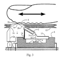
- Figure 3 shows a cross sectional view of another practical embodiment of a fingerprint sensor, employing through-hole technology electronic components of linear array sensor package 8 and linear array LED light source 2 soldered to PCB 9.
- the linear array sensor 4 silicon chip is supported by sensor package 8, which also supports transparent platen 1.
- GRIN lens array 3 is fitted or otherwise attached to platen 1 such that the focal distance is appropriate for imaging the fingerprint onto linear array sensor 4.
- Platen 1 also serves as a cover for package 8, providing a sealed enclosure for linear sensor array 4.
- the top surface of platen 1 of the fingerprint sensor protrudes slightly through a hole in cover surface 12, which represents part of the sensor enclosure.
- the linear array LED light source 2 shines collimated sheet of light 2a upward into the transparent platen 1 where it is bounced by TIR or mirror reflection on interior surface 1c towards interior surface 1a.
- the skin of fingerprint 5 touches the exterior surface of the platen 1 above position 1a, which causes FTIR reflection of a linear strip of the fingerprint image 2b towards GRIN lens array 3.
- Light 2c from GRIN lens array 3 is reflected by TIR or a mirrored surface on the interior surface 1e of platen 1, and is then directed downward and focused across the width of linear array sensor 4. If a mirrored surface is employed at surface 1e, the reflective layer may be applied to the external surface of platen 1.
- the optical design shown in Figure 3 with a single TIR or mirrored reflection of the fingerprint image on the interior surface 1e of platen 1, causes the image of the fingerprint on linear array sensor 4 to be both foreshortened and directionally reversed in relation to the direction of motion of the fingerprint; the foreshortening and directional reversal are easily characterized and accommodated for by adjustments in the electronic readout of linear array sensor 4.
- FIG 3 also shows several refinements which improve performance.
- the top of platen 1 has a slightly raised strip 1b, made from silicone rubber or other flexible or rigid transparent material, which provides increased local pressure of the fingerprint on the platen and also increased optical contact between the fingerprint and the flexible top of the platen, improving image quality.
- Surface 1f of platen 1 is blackened to reduce stray light reaching linear array 4.
- surface 1g inside platen 1 acts as a barrier to eliminate stray light from beam 2a reaching linear array 4.
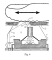
- Figure 4 shows a cross sectional view of another practical fingerprint sensor, employing through-hole technology electronic components: linear array sensor package 8 and linear array LED light source 2 soldered to PCB 9.
- the linear array sensor 4 silicon chip is supported by sensor package 8, which also supports transparent platen 1.
- GRIN lens array 3 is fitted or otherwise attached to platen 1.
- Platen 1 also serves as a cover for package 8, providing a sealed enclosure for linear sensor array 4 and GRIN lens array 3.
- the top surface of platen 1 of the fingerprint sensor protrudes slightly through a hole in cover surface 12, which encloses the sensor.
- the linear array LED light source 2 shines collimated sheet of light 2a upward into the transparent platen 1 where it is bounced by TIR on interior surface 1c towards interior surface 1a.
- the skin of fingerprint 5 touches the exterior surface of the platen 1 above position 1a, which causes FTIR reflection of a linear strip of the fingerprint image 2b towards interior surface 1d where it is reflected by TIR or a mirrored surface towards GRIN lens array 3. If a mirrored surface is employed at surface 1d, the reflective layer may be applied to the external surface of platen 1. Light 2c from GRIN lens array 3 is then directed downward and focused across the width of linear array sensor 4.
- the optical design shown in Figure 4 with a single TIR or mirror reflection of the fingerprint image on the interior surface 1d of platen 1, causes the image of the fingerprint on linear array sensor 4 to be both foreshortened and directionally reversed, in relation to the direction of motion of the fingerprint; the foreshortening and directional reversal are easily characterized and accommodated for by adjustments in the electronic readout of linear array sensor 4.
- Figure 4 also shows two optional refinements which can improve performance.
- Surface 1f of platen 1 is blackened to reduce stray light reaching linear array 4.
- Interior surface 1c of platen 1 is roughened to act as a reflective diffuser to light beam 2a to provide more constant illumination across the width of the fingerprint.
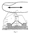
- Figure 5 shows a cross sectional view of another practical fingerprint sensor, employing through-hole technology electronic components of linear array sensor package 8 and linear array LED light source 2 soldered to PCB 9.
- the linear array sensor 4 silicon chip is supported by sensor package 8, which also supports transparent platen 1.
- Relay lens array 6 is fitted or otherwise attached inside platen 1 such that it projects an image of fingerprint 4 on linear array sensor 4.
- Platen 1 also serves as a cover for package 8, providing a sealed enclosure for linear sensor array 4 and relay lens array 6.
- the fingerprint image is acquired in a manner identical to Figure 4, with the exception that relay lens array 6 is used in place of a GRIN lens array.
- surface 1f of platen 1 is blackened to reduce stray light reaching linear array 4.
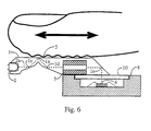
- Figure 6 shows a cross sectional view of a more compact fingerprint sensor.
- the linear array sensor 4 silicon chip is sealed inside sensor package 8 by transparent glass or plastic cover 10. Platen 1 is held in place over sensor package 8 and cover 10 by glue or other attachment or supporting means.
- GRIN lens array 3 and linear array LED light source 2 are fitted or otherwise attached to platen 1.
- Linear array LED light source 2 shines collimated light sheet 2a sideways into the transparent platen 1 where it is bounced by TIR or mirror reflection on interior surface 1c towards the top interior surface 1a of the transparent platen 1.
- the skin of fingerprint 5 touches the exterior surface of the platen 1 above position 1a, which causes a linear strip of the fingerprint image to be reflected by FTIR from 1a towards interior surface 1d, where it is again reflected by TIR or a mirror surface towards GRIN lens array 3.
- the light from GRIN lens array 3 is then reflected by TIR or mirror reflection by interior surface 1e, which then directs the light downward through cover 10 where the image is focused across the width of linear array sensor 4.
- the reflective layer may be applied to the external surface of platen 1.
- Figure 7 shows a cross sectional view of another compact fingerprint sensor, employing through-hole technology electronic components of linear array sensor package 8 and linear array LED light source 2 soldered to PCB 9.
- the linear array sensor 4 silicon chip is sealed inside sensor package 8 by transparent plastic or glass cover 10.
- Platen 1 is supported over cover 10 by glue or other attachment or support means.
- GRIN lens array 3 is fitted or otherwise attached to platen 1.
- Linear array LED light source 2 shines upward into the transparent platen 1, through curved surface 1h, which serves as a lens to collimate light inside platen 1, increasing the amount of light available for imaging the fingerprint.
- Light from light source 2 is bounced by TIR or mirror reflection on interior surface 1c towards the top interior surface 1a of the transparent platen 1.
- the skin of fingerprint 5 touches the exterior surface of the platen 1 above position 1a, which causes a linear strip of the fingerprint image to be reflected by FTIR from 1a towards interior surface 1d, where it is again reflected by TIR or mirror reflection towards GRIN lens array 3.
- the narrow strip image from GRIN lens array 3 is then reflected by TIR or mirror reflection on interior surface 1e, which directs the image downward through cover 10 where it is focused across the width of linear sensor array 4.
- the reflective layer may be applied to the external surface of platen 1.
- the upper interior surface 1a of the platen 1 is contained in a slightly raised strip 1b which provides increased pressure of the fingerprint onto the platen imaging surface above 1a, improving image quality.
- the image on linear array 4 is foreshortened but not reversed in direction.
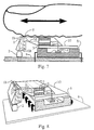
- Figure 8 shows a perspective view of the sensor shown in Figure 7, with the electronic components of linear array sensor package 8 and linear array LED light source 2 soldered to PCB 9; in this perspective view, the ends of the sensor package are cut off for display purposes.
- the width of the fingerprint sensor as measured along the width of transparent platen 1 and raised strip 1b, is about 19 mm, or the approximate width of the human finger, although variations in this dimension will also function satisfactorily.
- GRIN lens array 3 is at least the width of linear sensor array 4 and is fitted or otherwise attached to platen 1 to properly focus the fingerprint image on linear sensor array 4.
- Light source 2 can be seen as a linear bar of multiple linear array LEDs, or any other elongated light source, providing an upwardly directed sheet of approximately collimated light 2a, which is also the width of the fingerprint sensor.
- the sheet of light of light beam 2a is directed into platen 1 and reflected internally by TIR or mirror reflection at internal surface 1c in platen 1 onto interior surface 1a, illuminating the width of raised strip 1b of platen 1.
- the fingerprint ridges cause FTIR and absorb light at position 1a, while the valleys of the fingerprint do not touch the platen and thus allow light to be reflected by TIR from interior surface 1a.
- the narrow strip fingerprint image from the width surface 1a is reflected by TIR or mirror reflection along the width of interior surface 1d and is directed towards GRIN lens array 3.
- GRIN lens array 3 acts in the manner of a relay lens and refracts the fingerprint strip image and sends the image to be reflected again by TIR or mirror reflection along the width interior surface 1e, which then directs the image downward through glass or plastic cover 10 where the image of the narrow fingerprint strip is focused across the width of linear sensor array 4.
- the reflective layer may be applied to the external surface of platen 1.
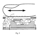
- Figure 9 shows a cross sectional view of a practical arrangement similar to that shown in Figure 7, employing through-hole technology electronic components of linear array sensor package 8 and linear array LED light source 2 soldered to PCB 9.
- the function of the transparent platen is separated into two parts.
- Platen 1 is attached to cover 10 by glue or other attachment means.
- the linear array sensor 4 silicon chip is sealed inside sensor package 8 by transparent plastic or glass cover 10, which also serves as part of the optical path to reflect the fingerprint image from interior surface 1e.
- GRIN lens array 3 is fitted or otherwise attached between platen 1 and cover 10; opaque layer 1f serves to limit unwanted light from reaching linear array sensor 4.
- the top surface of platen 1 of the fingerprint sensor protrudes slightly through a hole in cover surface 12, which is part of an enclosure for the sensor.
- Linear array LED light source 2 shines upward into the transparent platen 1.
- the collimated sheet of light 2a is bounced by TIR or mirror reflection on interior surface 1c towards top interior surface 1a of the transparent platen 1.
- the skin of fingerprint 5 touches the exterior surface of the platen 1 above position 1a, which causes a linear strip of the fingerprint image to be reflected by FTIR from 1a towards interior surface 1d, where it is again reflected by TIR or mirror reflection towards GRIN lens array 3.
- the narrow strip image from GRIN lens array 3 is then reflected by TIR or mirror reflection on interior surface 1e, which directs the image downward through cover 10 where it is focused across the width of linear sensor array 4.
- the reflective layer may be applied to the external surface of platen 1.
- the image on linear array 4 is foreshortened but not reversed in direction.
- Figure 10 shows a cross sectional view of a practical miniaturized sensor, employing chip-on-board (COB) mounting with wire-bonding 4a for the linear array sensor 4 and SMT for the linear array LED light source 2, both attached to PCB 9.
- COB chip-on-board
- platen 1 is designed to be glued or otherwise attached to PCB 9 and to completely cover linear array sensor 4, protecting it from the environment.
- GRIN lens array 3 is fitted or otherwise attached to platen 1.
- the fingerprint is optically sensed in a manner identical to that shown in Figure 7.
- the upper interior surface 1a of the platen 1 is contained in a slightly raised strip 1b which provides increased pressure of the fingerprint onto the platen imaging surface above 1a, improving image quality.
- a sponge or other absorbent or capillary material 11 serves to supply a fluid to the skin of the fingerprint, providing increased optical contact with platen 1.
- the top surface of platen 1 of the fingerprint sensor protrudes slightly through a hole in cover surface 12, which encloses the sensor.
- Figure 11 show a cross sectional view of a practical sub-miniaturized fingerprint sensor.
- Components are mounted on both sides of PCB 9.
- linear array LED light source 2 which shines a sheet of light upward through a slotted hole 9a or multiple single holes.
- linear array sensor 4 which is mounted using "flip-chip” technology, which either bonds the chip to the printed circuit board with pressure-welds which also provide the required electrical contacts, or is mounted using special conductive glue to bond the electrical contacts and hold the chip to the printed circuit board; epoxy coating 4b, or other suitable material, may be used to protect linear array sensor 4.
- Figure 12 shows a cross sectional view of another practical fingerprint sensor, employing surface-mount technology electronic components of linear array sensor package 8 and linear array LED light source 2 soldered to PCB 9.
- the linear array sensor 4 silicon chip is supported by sensor package 8, which is sealed by transparent cover 10 which also supports transparent platen 1.
- GRIN lens array 3 is fitted or otherwise attached to platen 1 such that the focal distance is appropriate for imaging the fingerprint onto linear array sensor 4.
- the top surface of platen 1 of the fingerprint sensor protrudes slightly through a hole in cover surface 12, which represents part of the sensor enclosure.
- the linear array LED light source 2 shines through refractive surface 1h upward into the transparent platen 1 providing a substantially collimated sheet of light 2a that is substantially normal to the interior platen surface 1a.
- the skin of fingerprint 5 touches the exterior surface of the platen 1 above position 1a, which causes the fingerprint ridges to glow from light source 2a.
- the GRIN lens array 3 views a linear strip of the fingerprint image at 1a along light path 2b.
- the fingerprint image from 1a is not viewed by means of TIR or FTIR, but rather by scattered light from the fingerprint ridges.
- a high contrast image of the fingerprint is obtained by positioning the GRIN lens to view platen surface 1a at an oblique angle, typically 45 degrees, so that very little light from the fingerprint valleys is transmitted.
- Light 2c from GRIN lens array 3 is reflected by TIR or a mirrored surface on the interior surface 1e of platen 1, and is then directed downward and focused across the width of linear array sensor 4.
- the reflective layer may be applied to the external surface of platen 1.
- the optical design shown in Figure 12 with a single TIR or mirrored reflection of the fingerprint image on the interior surface 1e of platen 1, causes the image of the fingerprint on linear array sensor 4 to be both foreshortened and directionally reversed in relation to the direction of motion of the fingerprint; the foreshortening and directional reversal are easily characterized and accommodated for by adjustments in the electronic readout of linear array sensor 4.
- Figure 12 also shows several optional refinements which improve performance.
- Surface 1f of platen 1 is blackened to reduce stray light reaching linear array 4 when no finger is present on platen 1.
- surface 1g inside platen 1 acts as a barrier to eliminate stray light from beam 2a reaching linear array 4.
- apparatus are examples of means to implement the method of creating an electronic image of a finger.
Abstract
Description
Claims (12)
- Imaging apparatus, including a platen (1) composed of a transparent material with an exterior surface for the skin of a finger and an opposed interior surface; a light source (2), for directing light to or reflecting light off said interior surface of said platen adjacent to the skin of the finger; a linear sensor array (4); and a GRIN lens array (3), for focusing the light from the top interior surface of the platen onto the linear sensor array;
characterized in that:(a) said exterior surface of said platen (1) having one and only one raised portion (1b); and(b) said GRIN lens array (3) situated at an oblique angle with respect to said platen (1). - Imaging apparatus, including a platen (1) composed of a transparent material with an exterior surface for the skin of a finger and an opposed interior surface; a light source (2), for directing light to or reflecting light off said interior surface of said platen adjacent to the skin of the finger; a linear sensor array (4); and a relay lens array (3), for focusing the light from the top interior surface of the platen onto the linear sensor array;
characterized in that:(a) said exterior surface of said platen (1) having one and only one raised portion (1b); and(b) said relay lens array (3) situated at an oblique angle with respect to said platen (1). - Imaging apparatus of one of claims 1 or 2, further having multiple parallel linear sensor arrays.
- Imaging apparatus of one of claims 1 through 3, further having said light from said light source redirected by a reflection on an interior surface of the platen using a mirror or total internal reflection.
- Imaging apparatus of one of claims 1 through 4, further having the light from the light source redirected by a reflection on an interior surface of the platen which is roughened.
- Imaging apparatus of one of claims 1 through 5, further having the light from the light source collimated by a lens molded into the platen where the light enters.
- Imaging apparatus of one of claims 1 through 6, further having a ridge on the top of the platen, either formed from the platen material or a different optically transparent material.
- Imaging apparatus of one of claims 1 through 7, further having the light from the platen surface reflected on an interior surface using a mirror or total internal reflection before entering the focus means.
- Imaging apparatus of one of claims 1 through 8, further having the light from the focusing means reflected on an interior surface using a mirror or total internal reflection before arriving at the linear sensor array.
- Imaging apparatus of one of claims 1 through 9, further having a reservoir for liquid embedded in the platen surface.
- Imaging apparatus of one of claims 1 through 10, further having blackened faces on the platen.
- Imaging apparatus of one of claims 1 through 11 further employing a method of sensing and measuring finger motion speed and correcting for geometric errors in the electronic output image.
Applications Claiming Priority (3)
| Application Number | Priority Date | Filing Date | Title |
|---|---|---|---|
| US09/169,008 US6259108B1 (en) | 1998-10-09 | 1998-10-09 | Fingerprint image optical input apparatus |
| US169008 | 1998-10-09 | ||
| PCT/CA1999/000936 WO2000022565A1 (en) | 1998-10-09 | 1999-10-08 | Fingerprint image optical input apparatus |
Publications (2)
| Publication Number | Publication Date |
|---|---|
| EP1119824A1 EP1119824A1 (en) | 2001-08-01 |
| EP1119824B1 true EP1119824B1 (en) | 2005-08-10 |
Family
ID=22613902
Family Applications (1)
| Application Number | Title | Priority Date | Filing Date |
|---|---|---|---|
| EP99947151A Expired - Lifetime EP1119824B1 (en) | 1998-10-09 | 1999-10-08 | Fingerprint image optical input apparatus |
Country Status (9)
| Country | Link |
|---|---|
| US (2) | US6259108B1 (en) |
| EP (1) | EP1119824B1 (en) |
| JP (1) | JP2002527832A (en) |
| KR (1) | KR100668361B1 (en) |
| AT (1) | ATE301853T1 (en) |
| AU (1) | AU6073599A (en) |
| CA (1) | CA2386973C (en) |
| DE (1) | DE69926645T2 (en) |
| WO (1) | WO2000022565A1 (en) |
Families Citing this family (174)
| Publication number | Priority date | Publication date | Assignee | Title |
|---|---|---|---|---|
| US6178255B1 (en) * | 1998-04-28 | 2001-01-23 | Cross Match Technologies, Inc. | Individualized fingerprint scanner |
| US6259108B1 (en) * | 1998-10-09 | 2001-07-10 | Kinetic Sciences Inc. | Fingerprint image optical input apparatus |
| US7268814B1 (en) * | 1999-10-05 | 2007-09-11 | California Institute Of Technology | Time-delayed-integration imaging with active pixel sensors |
| US6632512B1 (en) * | 1999-11-10 | 2003-10-14 | Ibiden Co., Ltd. | Ceramic substrate |
| US6538243B1 (en) * | 2000-01-04 | 2003-03-25 | Hewlett-Packard Company | Contact image sensor with light guide having least reflectivity near a light source |
| US20030016848A1 (en) * | 2000-03-08 | 2003-01-23 | Hideki Kitajima | Image reader |
| US6628377B1 (en) * | 2000-04-04 | 2003-09-30 | Stmicroelectronics, Inc. | Scanning optical semiconductor fingerprint detector |
| NO20003006L (en) * | 2000-06-09 | 2001-12-10 | Idex Asa | Mouse |
| US7289649B1 (en) * | 2000-08-10 | 2007-10-30 | Avago Technologies Ecbu Ip (Singapore) Pte. Ltd. | Fingerprint imager |
| EP1312040B1 (en) * | 2000-08-18 | 2006-04-05 | Cross Match Technologies, Inc. | Fingerprint scanner auto-capture system and method |
| ATE307362T1 (en) | 2000-12-05 | 2005-11-15 | Validity Sensors Inc | SYSTEM AND METHOD FOR CAPACITIVE CAPTURE OF FINGERPRINTS BY SCRUBING |
| US6928195B2 (en) * | 2000-12-18 | 2005-08-09 | Cross Match Technologies, Inc. | Palm scanner using a programmable nutating mirror for increased resolution |
| US7072034B2 (en) * | 2001-06-08 | 2006-07-04 | Kla-Tencor Corporation | Systems and methods for inspection of specimen surfaces |
| WO2002088878A2 (en) * | 2001-04-26 | 2002-11-07 | Cross Match Technologies, Inc. | Silicone rubber surfaces for biometric print tir prisms |
| US20020181750A1 (en) * | 2001-05-30 | 2002-12-05 | Kwell Hung | Fingerprint identification apparatus |
| JP2003006627A (en) * | 2001-06-18 | 2003-01-10 | Nec Corp | Fingerprint input device |
| CN1509895A (en) * | 2001-06-22 | 2004-07-07 | ��Τ����˹ | Color copying method |
| US7272248B2 (en) * | 2001-07-16 | 2007-09-18 | Activcard Ireland Limited | Biometric imaging device compensating for non-biometric parameters |
| JP4154874B2 (en) * | 2001-07-30 | 2008-09-24 | カシオ計算機株式会社 | Fingerprint reader and fingerprint reading method |
| US6646244B2 (en) * | 2001-12-19 | 2003-11-11 | Hewlett-Packard Development Company, L.P. | Optical imaging device with speed variable illumination |
| US20040032581A1 (en) * | 2002-01-15 | 2004-02-19 | Mehrdad Nikoonahad | Systems and methods for inspection of specimen surfaces |
| US6954260B2 (en) * | 2002-01-17 | 2005-10-11 | Cross Match Technologies, Inc. | Systems and methods for illuminating a platen in a print scanner |
| EP1476841B1 (en) | 2002-01-17 | 2008-08-27 | Cross Match Technologies, Inc. | Fingerprint workstation and methods |
| US6867850B2 (en) * | 2002-01-17 | 2005-03-15 | Cross Match Technologies, Inc. | Light wedge for illuminating a platen in a print scanner |
| US7088872B1 (en) * | 2002-02-14 | 2006-08-08 | Cogent Systems, Inc. | Method and apparatus for two dimensional image processing |
| JP2003242489A (en) * | 2002-02-20 | 2003-08-29 | Canon Inc | Image input device and fingerprint recognizing device |
| TWI243339B (en) * | 2002-03-19 | 2005-11-11 | Casio Computer Co Ltd | Image reading apparatus and drive control method |
| EP1353292B1 (en) * | 2002-04-12 | 2011-10-26 | STMicroelectronics (Research & Development) Limited | Biometric sensor apparatus and methods |
| US7073711B2 (en) * | 2002-04-19 | 2006-07-11 | Cross Match Technologies, Inc. | Mobile handheld code reader and print scanner system and method |
| US7079007B2 (en) * | 2002-04-19 | 2006-07-18 | Cross Match Technologies, Inc. | Systems and methods utilizing biometric data |
| US7019872B2 (en) * | 2002-06-19 | 2006-03-28 | Hewlett-Packard Development Company, L.P. | Compact scanner and scanning method |
| AU2003254280A1 (en) * | 2002-08-02 | 2004-02-23 | Cross Match Technologies, Inc. | System and method for counting ridges in a captured print image |
| US20040028262A1 (en) * | 2002-08-09 | 2004-02-12 | Kuo-Liang Lin | Optical system of fingerprint image capture apparatus |
| TW200403596A (en) * | 2002-08-27 | 2004-03-01 | Matsushita Electric Ind Co Ltd | Optical devices and optical reading apparatus |
| JP3859673B2 (en) * | 2002-09-17 | 2006-12-20 | 富士通株式会社 | Biometric information acquisition device and biometric information authentication device |
| US6904326B2 (en) * | 2002-10-17 | 2005-06-07 | Hewlett-Packard Development Company, Lp. | Light responsive data entry system |
| US20040101172A1 (en) * | 2002-11-26 | 2004-05-27 | Stmicroelectronics, Inc. | Imaging system with locator bar for accurate fingerprint recognition |
| EP1437677A1 (en) * | 2002-12-30 | 2004-07-14 | Nokia Corporation | Optical user interface for controlling portable electric device |
| US7164440B2 (en) * | 2003-02-28 | 2007-01-16 | Cross Match Technologies, Inc. | Dynamic image adaptation method for adjusting the quality of digital prints |
| JP2005038406A (en) * | 2003-06-27 | 2005-02-10 | Canon Inc | Fingerprint input apparatus and personal identification system using it |
| JP2005018594A (en) * | 2003-06-27 | 2005-01-20 | Canon Inc | Fingerprint input device, its manufacturing method, and personal identification system |
| JP3891572B2 (en) * | 2003-06-30 | 2007-03-14 | キヤノン株式会社 | Fingerprint input device, personal authentication system and electronic device |
| DE60327664D1 (en) * | 2003-08-13 | 2009-06-25 | Hitachi Ltd | PERSONAL IDENTIFICATION DEVICE |
| US20050047631A1 (en) * | 2003-08-26 | 2005-03-03 | Cross Match Technologies, Inc. | Method and apparatus for rolled fingerprint image capture with variable blending |
| CA2552650C (en) * | 2004-01-07 | 2014-09-30 | Identification International, Inc. | Low power fingerprint capture system, apparatus, and method |
| JP2005198843A (en) * | 2004-01-15 | 2005-07-28 | Mitsumi Electric Co Ltd | Image detector |
| EP1754180A1 (en) * | 2004-04-16 | 2007-02-21 | Validity Sensors Inc. | Finger position sensing methods and apparatus |
| US8175345B2 (en) | 2004-04-16 | 2012-05-08 | Validity Sensors, Inc. | Unitized ergonomic two-dimensional fingerprint motion tracking device and method |
| US7751601B2 (en) | 2004-10-04 | 2010-07-06 | Validity Sensors, Inc. | Fingerprint sensing assemblies and methods of making |
| US8447077B2 (en) | 2006-09-11 | 2013-05-21 | Validity Sensors, Inc. | Method and apparatus for fingerprint motion tracking using an in-line array |
| US8131026B2 (en) | 2004-04-16 | 2012-03-06 | Validity Sensors, Inc. | Method and apparatus for fingerprint image reconstruction |
| US8358815B2 (en) | 2004-04-16 | 2013-01-22 | Validity Sensors, Inc. | Method and apparatus for two-dimensional finger motion tracking and control |
| US8165355B2 (en) | 2006-09-11 | 2012-04-24 | Validity Sensors, Inc. | Method and apparatus for fingerprint motion tracking using an in-line array for use in navigation applications |
| US8229184B2 (en) | 2004-04-16 | 2012-07-24 | Validity Sensors, Inc. | Method and algorithm for accurate finger motion tracking |
| EP1747525A2 (en) * | 2004-04-23 | 2007-01-31 | Validity Sensors Inc. | Methods and apparatus for acquiring a swiped fingerprint image |
| GB0415447D0 (en) * | 2004-07-09 | 2004-08-11 | Tiger Telematics Inc | Portable electronic device |
| EP1782173A1 (en) * | 2004-07-29 | 2007-05-09 | Crucialtec Co., Ltd. | Optical pointing apparatus and personal portable device having the optical pointing apparatus |
| TW200612353A (en) * | 2004-10-15 | 2006-04-16 | Lite On Semiconductor Corp | Optical sensing module, optical sensing, image-capturing structure and optical print sensing method of handheld communication system |
| US7616788B2 (en) * | 2004-11-12 | 2009-11-10 | Cogent Systems, Inc. | System and method for fast biometric pattern matching |
| US7558410B2 (en) * | 2004-12-01 | 2009-07-07 | Ultra-Scan Corporation | Fingerprint scanning station |
| TWM267551U (en) * | 2004-12-21 | 2005-06-11 | Lite On Semiconductor Corp | Contact image sensing module with fingerprint scanning function |
| TWM268675U (en) * | 2004-12-24 | 2005-06-21 | Lite On Semiconductor Corp | Touch type image sensing module with motion detection function |
| JP4582406B2 (en) * | 2004-12-28 | 2010-11-17 | ソニー株式会社 | Biological imaging device |
| TWM268676U (en) * | 2004-12-28 | 2005-06-21 | Lite On Semiconductor Corp | Fingerprint scan device and electric equipment with fingerprint scan function |
| US7705835B2 (en) * | 2005-03-28 | 2010-04-27 | Adam Eikman | Photonic touch screen apparatus and method of use |
| US20060250605A1 (en) * | 2005-05-04 | 2006-11-09 | Chuan Liang Industrial Co., Ltd. | Compact-thin contact image sensor |
| US7460697B2 (en) * | 2005-07-19 | 2008-12-02 | Validity Sensors, Inc. | Electronic fingerprint sensor with differential noise cancellation |
| KR100760061B1 (en) | 2005-07-25 | 2007-09-18 | 추안 리앙 인더스트리얼 코., 엘티디. | Fingerprint identification assembly using total reflection to identify pattern of the fingerprint |
| EP2196944B1 (en) * | 2005-10-18 | 2014-10-01 | Authentec Inc. | Finger sensor including flexible circuit and associated methods |
| US8131477B2 (en) | 2005-11-16 | 2012-03-06 | 3M Cogent, Inc. | Method and device for image-based biological data quantification |
| JP4873533B2 (en) | 2005-12-15 | 2012-02-08 | 富士通株式会社 | High-speed serial transfer device test method, program and apparatus |
| JP4740743B2 (en) | 2006-01-06 | 2011-08-03 | 富士通株式会社 | Biological information input device |
| KR100729007B1 (en) * | 2006-01-19 | 2007-06-14 | 일렉비젼 인크. | Contact image capturing structure |
| RU2412460C2 (en) * | 2006-04-10 | 2011-02-20 | Электролюкс Хоум Продактс Корпорейшн Н.В. | Household electric appliance incorporating fingerprint identification sensor |
| TW200744000A (en) * | 2006-05-18 | 2007-12-01 | Pixart Imaging Inc | Optical module with a linear sensor for identifying images |
| US7671976B2 (en) * | 2006-06-05 | 2010-03-02 | Lockheed Martin Corporation | Systems and methods of using a flexible imaging surface to capture a rolled fingerprint |
| JP5007082B2 (en) * | 2006-08-04 | 2012-08-22 | 日立マクセル株式会社 | Imaging device and biometric authentication device |
| JP2008065440A (en) * | 2006-09-05 | 2008-03-21 | Fuji Denki Kogyo Kk | Fingerprint authentication device |
| JP4864632B2 (en) * | 2006-10-12 | 2012-02-01 | 株式会社リコー | Image input device, image input method, personal authentication device, and electronic device |
| JP4341670B2 (en) * | 2006-11-17 | 2009-10-07 | ミツミ電機株式会社 | Image input device |
| KR100917598B1 (en) * | 2006-11-24 | 2009-09-17 | 한국전자통신연구원 | Contact image sensor |
| US7812936B2 (en) * | 2007-04-09 | 2010-10-12 | Identification International, Inc. | Fingerprint imaging system |
| US8107212B2 (en) | 2007-04-30 | 2012-01-31 | Validity Sensors, Inc. | Apparatus and method for protecting fingerprint sensing circuitry from electrostatic discharge |
| US8275179B2 (en) * | 2007-05-01 | 2012-09-25 | 3M Cogent, Inc. | Apparatus for capturing a high quality image of a moist finger |
| US8290150B2 (en) | 2007-05-11 | 2012-10-16 | Validity Sensors, Inc. | Method and system for electronically securing an electronic device using physically unclonable functions |
| US8411916B2 (en) * | 2007-06-11 | 2013-04-02 | 3M Cogent, Inc. | Bio-reader device with ticket identification |
| EP2587345A3 (en) | 2007-08-19 | 2013-06-26 | Ringbow Ltd. | Finger-worn devices and related methods of use |
| US20100256489A1 (en) * | 2007-09-28 | 2010-10-07 | Nivasonix, Llc | Handheld Transducer Scanning Speed Guides and Position Detectors |
| US8204281B2 (en) | 2007-12-14 | 2012-06-19 | Validity Sensors, Inc. | System and method to remove artifacts from fingerprint sensor scans |
| US8276816B2 (en) | 2007-12-14 | 2012-10-02 | Validity Sensors, Inc. | Smart card system with ergonomic fingerprint sensor and method of using |
| DE102008017125A1 (en) * | 2008-04-03 | 2009-10-15 | Rudi Schael | Light scanning system, has objectives equipped with component that produces additional image rotation apart from natural image rotation with which both partial illustration and total illustration comprise identical image of scanning line |
| US8116540B2 (en) | 2008-04-04 | 2012-02-14 | Validity Sensors, Inc. | Apparatus and method for reducing noise in fingerprint sensing circuits |
| US8005276B2 (en) | 2008-04-04 | 2011-08-23 | Validity Sensors, Inc. | Apparatus and method for reducing parasitic capacitive coupling and noise in fingerprint sensing circuits |
| DE102008029467A1 (en) * | 2008-06-20 | 2009-12-24 | Osram Opto Semiconductors Gmbh | Semiconductor device, use of a semiconductor device as a proximity sensor and method for detecting objects |
| EP2321764A4 (en) | 2008-07-22 | 2012-10-10 | Validity Sensors Inc | System, device and method for securing a device component |
| US8391568B2 (en) | 2008-11-10 | 2013-03-05 | Validity Sensors, Inc. | System and method for improved scanning of fingerprint edges |
| US8278946B2 (en) | 2009-01-15 | 2012-10-02 | Validity Sensors, Inc. | Apparatus and method for detecting finger activity on a fingerprint sensor |
| US8600122B2 (en) | 2009-01-15 | 2013-12-03 | Validity Sensors, Inc. | Apparatus and method for culling substantially redundant data in fingerprint sensing circuits |
| US8374407B2 (en) | 2009-01-28 | 2013-02-12 | Validity Sensors, Inc. | Live finger detection |
| US8605960B2 (en) * | 2009-03-02 | 2013-12-10 | Avago Technologies General Ip (Singapore) Pte. Ltd. | Fingerprint sensing device |
| US8124953B2 (en) * | 2009-03-12 | 2012-02-28 | Infineon Technologies Ag | Sensor device having a porous structure element |
| CN101848299B (en) * | 2009-03-26 | 2014-04-16 | 海德堡印刷机械股份公司 | Device for imaging a flat object |
| GB2470554A (en) * | 2009-05-26 | 2010-12-01 | St Microelectronics Ltd | Optical navigation device with housing and optical transmission element to a mousing surface |
| GB2470553A (en) * | 2009-05-26 | 2010-12-01 | St Microelectronics Ltd | Optical computer input with single frustrated total internal reflection mousing surface |
| TWM372050U (en) * | 2009-09-09 | 2010-01-01 | Azurewave Technologies Inc | Image capturing module capable of simplifying optical component |
| TWM377018U (en) * | 2009-09-09 | 2010-03-21 | Azurewave Technologies Inc | Flip chip type image capturing module |
| US9336428B2 (en) | 2009-10-30 | 2016-05-10 | Synaptics Incorporated | Integrated fingerprint sensor and display |
| US9400911B2 (en) | 2009-10-30 | 2016-07-26 | Synaptics Incorporated | Fingerprint sensor and integratable electronic display |
| US9274553B2 (en) | 2009-10-30 | 2016-03-01 | Synaptics Incorporated | Fingerprint sensor and integratable electronic display |
| US9280695B2 (en) * | 2009-11-11 | 2016-03-08 | Cross Match Technologies, Inc. | Apparatus and method for determining sequencing of fingers in images to a two-finger scanner of fingerprint images |
| JP4842363B2 (en) * | 2009-11-17 | 2011-12-21 | シャープ株式会社 | Pointing device and electronic device |
| US8791792B2 (en) | 2010-01-15 | 2014-07-29 | Idex Asa | Electronic imager using an impedance sensor grid array mounted on or about a switch and method of making |
| US8866347B2 (en) | 2010-01-15 | 2014-10-21 | Idex Asa | Biometric image sensing |
| US8421890B2 (en) | 2010-01-15 | 2013-04-16 | Picofield Technologies, Inc. | Electronic imager using an impedance sensor grid array and method of making |
| TW201126385A (en) * | 2010-01-25 | 2011-08-01 | Maxemil Photonics Corp | Optical position indication input apparatus |
| US9666635B2 (en) | 2010-02-19 | 2017-05-30 | Synaptics Incorporated | Fingerprint sensing circuit |
| US8716613B2 (en) | 2010-03-02 | 2014-05-06 | Synaptics Incoporated | Apparatus and method for electrostatic discharge protection |
| US9001040B2 (en) | 2010-06-02 | 2015-04-07 | Synaptics Incorporated | Integrated fingerprint sensor and navigation device |
| US8331096B2 (en) | 2010-08-20 | 2012-12-11 | Validity Sensors, Inc. | Fingerprint acquisition expansion card apparatus |
| JP2012133455A (en) * | 2010-12-20 | 2012-07-12 | Mitsumi Electric Co Ltd | Pointing device |
| US8594393B2 (en) | 2011-01-26 | 2013-11-26 | Validity Sensors | System for and method of image reconstruction with dual line scanner using line counts |
| US8538097B2 (en) | 2011-01-26 | 2013-09-17 | Validity Sensors, Inc. | User input utilizing dual line scanner apparatus and method |
| GB2489100A (en) | 2011-03-16 | 2012-09-19 | Validity Sensors Inc | Wafer-level packaging for a fingerprint sensor |
| US9082188B2 (en) * | 2011-04-11 | 2015-07-14 | Hid Global Corporation | Optical topographic imaging |
| GB201110218D0 (en) | 2011-06-16 | 2011-08-03 | St Microelectronics Res & Dev | Optical navigation device |
| US10043052B2 (en) | 2011-10-27 | 2018-08-07 | Synaptics Incorporated | Electronic device packages and methods |
| US9195877B2 (en) | 2011-12-23 | 2015-11-24 | Synaptics Incorporated | Methods and devices for capacitive image sensing |
| US9785299B2 (en) | 2012-01-03 | 2017-10-10 | Synaptics Incorporated | Structures and manufacturing methods for glass covered electronic devices |
| US9251329B2 (en) | 2012-03-27 | 2016-02-02 | Synaptics Incorporated | Button depress wakeup and wakeup strategy |
| US9137438B2 (en) | 2012-03-27 | 2015-09-15 | Synaptics Incorporated | Biometric object sensor and method |
| US9268991B2 (en) | 2012-03-27 | 2016-02-23 | Synaptics Incorporated | Method of and system for enrolling and matching biometric data |
| US9600709B2 (en) | 2012-03-28 | 2017-03-21 | Synaptics Incorporated | Methods and systems for enrolling biometric data |
| US9152838B2 (en) | 2012-03-29 | 2015-10-06 | Synaptics Incorporated | Fingerprint sensor packagings and methods |
| US20130279769A1 (en) | 2012-04-10 | 2013-10-24 | Picofield Technologies Inc. | Biometric Sensing |
| TWI518306B (en) * | 2012-10-04 | 2016-01-21 | 原相科技股份有限公司 | Image retrieving device and optical motion estimation device |
| EP2930919A4 (en) | 2012-12-06 | 2016-08-10 | Mitsubishi Electric Corp | Image read-in device |
| US9665762B2 (en) | 2013-01-11 | 2017-05-30 | Synaptics Incorporated | Tiered wakeup strategy |
| WO2014119503A1 (en) * | 2013-01-31 | 2014-08-07 | 日本電気株式会社 | Authentication device, prism body for authentication, and authentication method |
| CN105392722B (en) * | 2013-03-08 | 2017-06-09 | 胶视公司 | Continuous three-dimensional measurement based on contact |
| US9136258B1 (en) * | 2013-11-26 | 2015-09-15 | Maxim Integrated Products, Inc. | Stacked LED for optical sensor devices |
| US9773151B2 (en) | 2014-02-06 | 2017-09-26 | University Of Massachusetts | System and methods for contactless biometrics-based identification |
| US10713521B2 (en) * | 2016-08-05 | 2020-07-14 | Gingy Technology Inc. | Image capturing apparatus and manufacturing method thereof |
| FR3027730B1 (en) * | 2014-10-22 | 2017-12-22 | New Imaging Tech | DEVICE FOR ACQUIRING DIGITAL IMPRESSIONS |
| US10192856B2 (en) * | 2014-12-30 | 2019-01-29 | Pixart Imaging Inc. | Optical navigation module capable of performing lateral detection and adjusting tracking distance |
| US9829614B2 (en) | 2015-02-02 | 2017-11-28 | Synaptics Incorporated | Optical sensor using collimator |
| US10181070B2 (en) | 2015-02-02 | 2019-01-15 | Synaptics Incorporated | Low profile illumination in an optical fingerprint sensor |
| CN104751121B (en) * | 2015-03-05 | 2019-04-05 | 上海交通大学 | Light wave conduction fingerprint recognition system based on optical grating construction |
| USD776664S1 (en) * | 2015-05-20 | 2017-01-17 | Chaya Coleena Hendrick | Smart card |
| US9915776B2 (en) * | 2015-09-04 | 2018-03-13 | Concraft Holding Co., Ltd. | Light guide mechanism of fingerprint recognition plate |
| US10614281B2 (en) | 2015-09-15 | 2020-04-07 | Shanghai Oxi Technology Co., Ltd | Optical fingerprint imaging system and array sensor |
| WO2017049318A1 (en) * | 2015-09-18 | 2017-03-23 | Synaptics Incorporated | Optical fingerprint sensor package |
| US9934418B2 (en) * | 2015-12-03 | 2018-04-03 | Synaptics Incorporated | Display integrated optical fingerprint sensor with angle limiting reflector |
| US10169630B2 (en) | 2015-12-03 | 2019-01-01 | Synaptics Incorporated | Optical sensor for integration over a display backplane |
| US10176355B2 (en) | 2015-12-03 | 2019-01-08 | Synaptics Incorporated | Optical sensor for integration in a display |
| CN105354561A (en) * | 2015-12-08 | 2016-02-24 | 开发晶照明(厦门)有限公司 | Fingerprint image acquisition apparatus |
| KR102091657B1 (en) * | 2015-12-11 | 2020-04-23 | 주식회사 이랜텍 | method for manufacturing the camera module package |
| US10282583B2 (en) | 2015-12-22 | 2019-05-07 | Gemalto Sa | Fingerprint imaging systems comprising self-wetting adhesive, films and methods |
| US9454259B2 (en) | 2016-01-04 | 2016-09-27 | Secugen Corporation | Multi-level command sensing apparatus |
| WO2017198764A1 (en) * | 2016-05-20 | 2017-11-23 | Sentech Instruments Gmbh | Device and method for measuring layer thicknesses and indices of refraction of layers on rough and smooth surfaces |
| TWI584201B (en) * | 2016-07-17 | 2017-05-21 | 金佶科技股份有限公司 | Identification apparatus and identification method |
| TWI664578B (en) * | 2016-08-05 | 2019-07-01 | Gingy Technology Inc. | Image capturing apparatus and manufacturing method thereof |
| WO2018064563A1 (en) * | 2016-09-29 | 2018-04-05 | Synaptics Incorporated | Low profile illumination in an optical fingerprint sensor |
| KR20180039222A (en) | 2016-10-07 | 2018-04-18 | 삼성디스플레이 주식회사 | Display device comprising fingerprint sensor |
| RU2742966C2 (en) * | 2016-10-18 | 2021-02-12 | Конинклейке Филипс Н.В. | Auxiliary device and visualization device |
| CN108009467A (en) * | 2016-10-27 | 2018-05-08 | 金佶科技股份有限公司 | Image capturing device and manufacturing method thereof |
| CN108241833A (en) * | 2016-12-23 | 2018-07-03 | 创智能科技股份有限公司 | Biometric recognition device.It |
| TWI649696B (en) * | 2017-01-13 | 2019-02-01 | 致伸科技股份有限公司 | Fingerprint identifying module with indicating function |
| CN108304751A (en) * | 2017-01-13 | 2018-07-20 | 致伸科技股份有限公司 | Identification of fingerprint module with instruction function |
| US10235557B1 (en) * | 2018-01-08 | 2019-03-19 | Secugen Corporation | Method and apparatus for sensing fingerprint |
| KR102195081B1 (en) * | 2019-03-12 | 2020-12-24 | (주)파트론 | Fingerprint recognition sensor package |
| KR102195088B1 (en) * | 2019-04-17 | 2020-12-24 | (주)파트론 | Fingerprint recognition sensor package |
| KR20210019641A (en) | 2019-08-12 | 2021-02-23 | 삼성전자주식회사 | Biometric information sensing module and electronic device including the same |
| CN112449034A (en) * | 2019-08-30 | 2021-03-05 | 北京小米移动软件有限公司 | Mobile terminal |
| DE102021112447A1 (en) * | 2021-05-12 | 2022-11-17 | Infineon Technologies Ag | Smart card biometrics sensor device, smart card, method of forming a smart card biometrics sensor device and method of forming a smart card |
Family Cites Families (14)
| Publication number | Priority date | Publication date | Assignee | Title |
|---|---|---|---|---|
| CA1187997A (en) | 1982-07-09 | 1985-05-28 | Inc. Fingermatrix | Fingerprint image refinement |
| US4832485A (en) | 1982-09-03 | 1989-05-23 | Commonwealth Technology, Inc. | Image enhancer |
| DK155242C (en) * | 1985-05-02 | 1989-07-31 | Jydsk Telefon As | METHOD AND APPARATUS FOR AUTOMATIC DETECTION OF FINGERPRINT |
| JPH0648494B2 (en) * | 1987-04-28 | 1994-06-22 | 富士通株式会社 | Uneven surface information input device |
| US5619586A (en) * | 1990-12-20 | 1997-04-08 | Thorn Emi Plc | Method and apparatus for producing a directly viewable image of a fingerprint |
| JPH07325901A (en) * | 1991-03-18 | 1995-12-12 | Fujitsu Ltd | Fingerprint sensor |
| US5448649A (en) | 1994-05-24 | 1995-09-05 | Chen; Wang S. | Apparatus for imaging fingerprint or topographic relief pattern on the surface of an object |
| US5596454A (en) | 1994-10-28 | 1997-01-21 | The National Registry, Inc. | Uneven surface image transfer apparatus |
| JPH08154921A (en) * | 1994-12-06 | 1996-06-18 | Nippon Telegr & Teleph Corp <Ntt> | Finger print camera apparatus |
| JPH08279035A (en) * | 1995-04-06 | 1996-10-22 | Nippon Telegr & Teleph Corp <Ntt> | Fingerprint input device |
| US5942761A (en) * | 1995-06-07 | 1999-08-24 | Tuli; Raja Singh | Enhancement methods and devices for reading a fingerprint image |
| JPH09198495A (en) * | 1996-01-16 | 1997-07-31 | Micro Net:Kk | Fingerprint image pickup device for fingerprint collator |
| JPH10289304A (en) * | 1997-02-12 | 1998-10-27 | Nec Corp | Fingerprint image input device |
| US6259108B1 (en) * | 1998-10-09 | 2001-07-10 | Kinetic Sciences Inc. | Fingerprint image optical input apparatus |
-
1998
- 1998-10-09 US US09/169,008 patent/US6259108B1/en not_active Expired - Lifetime
-
1999
- 1999-10-08 AT AT99947151T patent/ATE301853T1/en not_active IP Right Cessation
- 1999-10-08 WO PCT/CA1999/000936 patent/WO2000022565A1/en not_active Application Discontinuation
- 1999-10-08 JP JP2000576403A patent/JP2002527832A/en active Pending
- 1999-10-08 AU AU60735/99A patent/AU6073599A/en not_active Abandoned
- 1999-10-08 CA CA002386973A patent/CA2386973C/en not_active Expired - Fee Related
- 1999-10-08 DE DE69926645T patent/DE69926645T2/en not_active Expired - Lifetime
- 1999-10-08 KR KR1020017004506A patent/KR100668361B1/en not_active IP Right Cessation
- 1999-10-08 EP EP99947151A patent/EP1119824B1/en not_active Expired - Lifetime
-
2001
- 2001-04-09 US US09/833,262 patent/US6355937B2/en not_active Expired - Lifetime
Also Published As
| Publication number | Publication date |
|---|---|
| US20010050765A1 (en) | 2001-12-13 |
| US6355937B2 (en) | 2002-03-12 |
| KR20010088861A (en) | 2001-09-28 |
| KR100668361B1 (en) | 2007-01-12 |
| WO2000022565A1 (en) | 2000-04-20 |
| US6259108B1 (en) | 2001-07-10 |
| EP1119824A1 (en) | 2001-08-01 |
| DE69926645T2 (en) | 2006-06-08 |
| DE69926645D1 (en) | 2005-09-15 |
| JP2002527832A (en) | 2002-08-27 |
| CA2386973A1 (en) | 2000-04-20 |
| ATE301853T1 (en) | 2005-08-15 |
| AU6073599A (en) | 2000-05-01 |
| CA2386973C (en) | 2006-12-19 |
Similar Documents
| Publication | Publication Date | Title |
|---|---|---|
| EP1119824B1 (en) | Fingerprint image optical input apparatus | |
| KR100611135B1 (en) | Method and apparatus for illuminating a fingerprint | |
| US20050025346A1 (en) | Fingerprint input apparatus | |
| EP1131775B1 (en) | High contrast, low distortion optical acquisition system for image capturing | |
| US7244925B2 (en) | Compact and low profile optical navigation device | |
| US7732752B2 (en) | Continuous base beneath optical sensor and optical homodyning system | |
| US20060146175A1 (en) | Image capture module and image capture apparatus for inputting shape of object on three dimensional space | |
| US8558162B2 (en) | Optical pointing device having a transparent housing element | |
| US6265706B1 (en) | Edge to edge image sensor and navigator for portable scanner | |
| US20030016848A1 (en) | Image reader | |
| TW583588B (en) | Device for detecting movements of a surface of an object | |
| US7180643B2 (en) | Live print scanner with holographic imaging a different magnifications | |
| JP2980051B2 (en) | Fingerprint detection method and device | |
| JPH08154921A (en) | Finger print camera apparatus | |
| US6426498B1 (en) | Optics module for optical scanning device | |
| WO2001018741A1 (en) | A thin prism fingerprint imager system | |
| US7208719B2 (en) | Compact integrated optical imaging assembly | |
| US7206102B2 (en) | Image reading apparatus with partially shielded light-receiving elements | |
| JPH10257247A (en) | Image reader and scanner | |
| US20040227059A1 (en) | Compact integrated optical imaging assembly | |
| JPH0588068U (en) | Image sensor unit | |
| JPH0399576A (en) | Contact type image sensor | |
| JPH056423A (en) | Image reader | |
| JP2001283206A (en) | Image reader | |
| GB2387734A (en) | Portable document scanner having central linear image detector and position detectors. |
Legal Events
| Date | Code | Title | Description |
|---|---|---|---|
| PUAI | Public reference made under article 153(3) epc to a published international application that has entered the european phase |
Free format text: ORIGINAL CODE: 0009012 |
|
| 17P | Request for examination filed |
Effective date: 20010504 |
|
| AK | Designated contracting states |
Kind code of ref document: A1 Designated state(s): AT BE CH CY DE DK ES FI FR GB GR IE IT LI LU MC NL PT SE |
|
| 17Q | First examination report despatched |
Effective date: 20030915 |
|
| RAP1 | Party data changed (applicant data changed or rights of an application transferred) |
Owner name: KINETIC SCIENCES INC. |
|
| GRAP | Despatch of communication of intention to grant a patent |
Free format text: ORIGINAL CODE: EPIDOSNIGR1 |
|
| GRAS | Grant fee paid |
Free format text: ORIGINAL CODE: EPIDOSNIGR3 |
|
| GRAA | (expected) grant |
Free format text: ORIGINAL CODE: 0009210 |
|
| AK | Designated contracting states |
Kind code of ref document: B1 Designated state(s): AT BE CH CY DE DK ES FI FR GB GR IE IT LI LU MC NL PT SE |
|
| PG25 | Lapsed in a contracting state [announced via postgrant information from national office to epo] |
Ref country code: NL Free format text: LAPSE BECAUSE OF FAILURE TO SUBMIT A TRANSLATION OF THE DESCRIPTION OR TO PAY THE FEE WITHIN THE PRESCRIBED TIME-LIMIT Effective date: 20050810 Ref country code: LI Free format text: LAPSE BECAUSE OF FAILURE TO SUBMIT A TRANSLATION OF THE DESCRIPTION OR TO PAY THE FEE WITHIN THE PRESCRIBED TIME-LIMIT Effective date: 20050810 Ref country code: IT Free format text: LAPSE BECAUSE OF FAILURE TO SUBMIT A TRANSLATION OF THE DESCRIPTION OR TO PAY THE FEE WITHIN THE PRESCRIBED TIME-LIMIT;WARNING: LAPSES OF ITALIAN PATENTS WITH EFFECTIVE DATE BEFORE 2007 MAY HAVE OCCURRED AT ANY TIME BEFORE 2007. THE CORRECT EFFECTIVE DATE MAY BE DIFFERENT FROM THE ONE RECORDED. Effective date: 20050810 Ref country code: FI Free format text: LAPSE BECAUSE OF FAILURE TO SUBMIT A TRANSLATION OF THE DESCRIPTION OR TO PAY THE FEE WITHIN THE PRESCRIBED TIME-LIMIT Effective date: 20050810 Ref country code: CH Free format text: LAPSE BECAUSE OF FAILURE TO SUBMIT A TRANSLATION OF THE DESCRIPTION OR TO PAY THE FEE WITHIN THE PRESCRIBED TIME-LIMIT Effective date: 20050810 Ref country code: BE Free format text: LAPSE BECAUSE OF FAILURE TO SUBMIT A TRANSLATION OF THE DESCRIPTION OR TO PAY THE FEE WITHIN THE PRESCRIBED TIME-LIMIT Effective date: 20050810 Ref country code: AT Free format text: LAPSE BECAUSE OF FAILURE TO SUBMIT A TRANSLATION OF THE DESCRIPTION OR TO PAY THE FEE WITHIN THE PRESCRIBED TIME-LIMIT Effective date: 20050810 |
|
| REG | Reference to a national code |
Ref country code: GB Ref legal event code: FG4D |
|
| REG | Reference to a national code |
Ref country code: CH Ref legal event code: EP |
|
| REG | Reference to a national code |
Ref country code: IE Ref legal event code: FG4D |
|
| REF | Corresponds to: |
Ref document number: 69926645 Country of ref document: DE Date of ref document: 20050915 Kind code of ref document: P |
|
| PG25 | Lapsed in a contracting state [announced via postgrant information from national office to epo] |
Ref country code: CY Free format text: LAPSE BECAUSE OF FAILURE TO SUBMIT A TRANSLATION OF THE DESCRIPTION OR TO PAY THE FEE WITHIN THE PRESCRIBED TIME-LIMIT Effective date: 20051008 |
|
| PG25 | Lapsed in a contracting state [announced via postgrant information from national office to epo] |
Ref country code: IE Free format text: LAPSE BECAUSE OF NON-PAYMENT OF DUE FEES Effective date: 20051010 |
|
| PG25 | Lapsed in a contracting state [announced via postgrant information from national office to epo] |
Ref country code: MC Free format text: LAPSE BECAUSE OF NON-PAYMENT OF DUE FEES Effective date: 20051031 Ref country code: LU Free format text: LAPSE BECAUSE OF NON-PAYMENT OF DUE FEES Effective date: 20051031 |
|
| PG25 | Lapsed in a contracting state [announced via postgrant information from national office to epo] |
Ref country code: SE Free format text: LAPSE BECAUSE OF FAILURE TO SUBMIT A TRANSLATION OF THE DESCRIPTION OR TO PAY THE FEE WITHIN THE PRESCRIBED TIME-LIMIT Effective date: 20051110 Ref country code: GR Free format text: LAPSE BECAUSE OF FAILURE TO SUBMIT A TRANSLATION OF THE DESCRIPTION OR TO PAY THE FEE WITHIN THE PRESCRIBED TIME-LIMIT Effective date: 20051110 Ref country code: DK Free format text: LAPSE BECAUSE OF FAILURE TO SUBMIT A TRANSLATION OF THE DESCRIPTION OR TO PAY THE FEE WITHIN THE PRESCRIBED TIME-LIMIT Effective date: 20051110 |
|
| PG25 | Lapsed in a contracting state [announced via postgrant information from national office to epo] |
Ref country code: ES Free format text: LAPSE BECAUSE OF FAILURE TO SUBMIT A TRANSLATION OF THE DESCRIPTION OR TO PAY THE FEE WITHIN THE PRESCRIBED TIME-LIMIT Effective date: 20051121 |
|
| PG25 | Lapsed in a contracting state [announced via postgrant information from national office to epo] |
Ref country code: PT Free format text: LAPSE BECAUSE OF FAILURE TO SUBMIT A TRANSLATION OF THE DESCRIPTION OR TO PAY THE FEE WITHIN THE PRESCRIBED TIME-LIMIT Effective date: 20060110 |
|
| NLV1 | Nl: lapsed or annulled due to failure to fulfill the requirements of art. 29p and 29m of the patents act | ||
| REG | Reference to a national code |
Ref country code: CH Ref legal event code: PL |
|
| ET | Fr: translation filed | ||
| PLBE | No opposition filed within time limit |
Free format text: ORIGINAL CODE: 0009261 |
|
| STAA | Information on the status of an ep patent application or granted ep patent |
Free format text: STATUS: NO OPPOSITION FILED WITHIN TIME LIMIT |
|
| 26N | No opposition filed |
Effective date: 20060511 |
|
| REG | Reference to a national code |
Ref country code: IE Ref legal event code: MM4A |
|
| PGFP | Annual fee paid to national office [announced via postgrant information from national office to epo] |
Ref country code: DE Payment date: 20091028 Year of fee payment: 11 |
|
| PGFP | Annual fee paid to national office [announced via postgrant information from national office to epo] |
Ref country code: GB Payment date: 20091026 Year of fee payment: 11 Ref country code: FR Payment date: 20091029 Year of fee payment: 11 |
|
| GBPC | Gb: european patent ceased through non-payment of renewal fee |
Effective date: 20101008 |
|
| PG25 | Lapsed in a contracting state [announced via postgrant information from national office to epo] |
Ref country code: FR Free format text: LAPSE BECAUSE OF NON-PAYMENT OF DUE FEES Effective date: 20101102 |
|
| REG | Reference to a national code |
Ref country code: FR Ref legal event code: ST Effective date: 20110630 |
|
| REG | Reference to a national code |
Ref country code: DE Ref legal event code: R119 Ref document number: 69926645 Country of ref document: DE Effective date: 20110502 |
|
| PG25 | Lapsed in a contracting state [announced via postgrant information from national office to epo] |
Ref country code: GB Free format text: LAPSE BECAUSE OF NON-PAYMENT OF DUE FEES Effective date: 20101008 |
|
| PG25 | Lapsed in a contracting state [announced via postgrant information from national office to epo] |
Ref country code: DE Free format text: LAPSE BECAUSE OF NON-PAYMENT OF DUE FEES Effective date: 20110502 |