EP1119104A1 - Power device with protection against undesirable self-activation - Google Patents
Power device with protection against undesirable self-activation Download PDFInfo
- Publication number
- EP1119104A1 EP1119104A1 EP00830028A EP00830028A EP1119104A1 EP 1119104 A1 EP1119104 A1 EP 1119104A1 EP 00830028 A EP00830028 A EP 00830028A EP 00830028 A EP00830028 A EP 00830028A EP 1119104 A1 EP1119104 A1 EP 1119104A1
- Authority
- EP
- European Patent Office
- Prior art keywords
- power device
- terminal
- protection circuit
- conduction terminal
- gate
- Prior art date
- Legal status (The legal status is an assumption and is not a legal conclusion. Google has not performed a legal analysis and makes no representation as to the accuracy of the status listed.)
- Granted
Links
- 238000001465 metallisation Methods 0.000 description 9
- 210000000746 body region Anatomy 0.000 description 4
- 238000000034 method Methods 0.000 description 4
- 238000010586 diagram Methods 0.000 description 3
- 230000008878 coupling Effects 0.000 description 2
- 238000010168 coupling process Methods 0.000 description 2
- 238000005859 coupling reaction Methods 0.000 description 2
- 239000012535 impurity Substances 0.000 description 2
- 230000010354 integration Effects 0.000 description 2
- 238000004519 manufacturing process Methods 0.000 description 2
- 230000015556 catabolic process Effects 0.000 description 1
- 230000002860 competitive effect Effects 0.000 description 1
- 230000007423 decrease Effects 0.000 description 1
- 238000002955 isolation Methods 0.000 description 1
- 238000012986 modification Methods 0.000 description 1
- 230000004048 modification Effects 0.000 description 1
- 229910021420 polycrystalline silicon Inorganic materials 0.000 description 1
- 229920005591 polysilicon Polymers 0.000 description 1
- 239000000758 substrate Substances 0.000 description 1
Images


Classifications
-
- H—ELECTRICITY
- H03—ELECTRONIC CIRCUITRY
- H03K—PULSE TECHNIQUE
- H03K17/00—Electronic switching or gating, i.e. not by contact-making and –breaking
- H03K17/08—Modifications for protecting switching circuit against overcurrent or overvoltage
- H03K17/082—Modifications for protecting switching circuit against overcurrent or overvoltage by feedback from the output to the control circuit
- H03K17/0822—Modifications for protecting switching circuit against overcurrent or overvoltage by feedback from the output to the control circuit in field-effect transistor switches
-
- H—ELECTRICITY
- H03—ELECTRONIC CIRCUITRY
- H03K—PULSE TECHNIQUE
- H03K17/00—Electronic switching or gating, i.e. not by contact-making and –breaking
- H03K17/08—Modifications for protecting switching circuit against overcurrent or overvoltage
- H03K17/081—Modifications for protecting switching circuit against overcurrent or overvoltage without feedback from the output circuit to the control circuit
- H03K17/0812—Modifications for protecting switching circuit against overcurrent or overvoltage without feedback from the output circuit to the control circuit by measures taken in the control circuit
- H03K17/08122—Modifications for protecting switching circuit against overcurrent or overvoltage without feedback from the output circuit to the control circuit by measures taken in the control circuit in field-effect transistor switches
Definitions
- the present invention regards a power device with protection against undesirable self-activation.
- power devices are able to manage high voltages and currents.
- external causes such as disturbances that are created on the supply networks, may lead to these quantities exceeding the maximum values that can be withstood by these devices or may even modify the electrical stability of the circuits in which these devices are inserted.
- a known power device 1 is shown in Figure 1 and comprises a vertical transistor of the MOS type having a gate terminal 2 and a source terminal 3 connected together via a diffused resistor 5 having a resistance R.
- the gate terminal 2 is also connected to a control unit 10, which is shown only schematically in Figure 1 and comprises known driving circuits which supply a driving signal to the power device 1.
- the diffused resistor 5 and the power device 1 are made in one and the same chip 20.
- the diffused resistor 5 is formed in the proximity of the gate pad of the power device 1 by doping, with N-type impurities, a polysilicon portion previously enriched with P-type impurities.
- the resistance R must have a high value. Specifically, when the gate terminal 2 receives the driving signal from the control unit 10, the value of the resistance R should be such as not to absorb the charge supplied to the gate terminal 2. On the other hand, when the control unit 10 does not supply the driving signal, thus leaving the gate terminal 2 floating, the resistance R should have a low value so as to short-circuit the gate terminal 2 and source terminal 3 of the power device 1, thus keeping it turned off. Since the two requirements referred to above are mutually incompatible, it is not possible to have a power device which operates correctly and is protected from self-activation.
- a first Zener diode 6 and a second Zener diode 7 are mutually connected in anti-series between a drain terminal 4 of the power device 1 and the gate terminal 2; in addition, a third Zener diode 8 and a fourth Zener diode 9 are mutually connected in anti-series between the gate terminal 2 and the source terminal 3 of the device itself.
- this circuit arrangement fails to prevent self-activation of the power device 1, given that the breakdown voltage of the Zener diodes 6 and 7 must be higher than the driving voltage required for turning on the power device 1 during normal operation.
- the present invention aims at solving the technical problems referred to above by providing a power device that is protected against undesirable self-activation.
- the power device of Figure 1 is equipped with a protection circuit 11 connected between the gate terminal 2 and the source terminal 3 of the device.
- a first embodiment of the protection circuit 11 comprises the diffused resistor 5 connected in series to an ON-OFF switch 12.
- the ON-OFF switch 12 is made using a MOS transistor of the horizontal type having a first conduction terminal connected, via the diffused resistor 5, to the gate terminal of the power device 1, a second conduction terminal connected to the source terminal 3 of the power device 1, and a control terminal connected to the drain terminal 4.
- the diffused resistor 5 is formed in the same chip 20 as the power device 1, in the vicinity of the gate pad of the device itself, and has a resistance R of approximately k ⁇ . Also made in the chip 20 is the MOS transistor 12, using two different integration techniques according to the maximum voltage value to which the power device 1 may be subjected.
- Figures 5 and 6 show cross sections of the chip 20 incorporating the MOS transistor 12, according to two different embodiments.
- the chip 20 comprises a substrate 13 on top of which an epitaxial layer 14 is formed.
- the epitaxial layer 14 houses a body region 15 of the MOS transistor 12, in which a drain region 16 and a source region 17 of the transistor itself are formed.
- the drain region 16 and the source region 17 are in electrical contact, respectively, with a drain metallization region 18 and with a source metallization region 19.
- Formed on top of the body region 15 is a gate region 30 isolated from the body region 15 by means of a gate oxide layer 21.
- An insulating dielectric 22 covers the gate region 30, insulating it from the drain metallization region 18 and the gate metallization region 19. Thick field-oxide portions 31, set at the sides of the body region 15, protect the edges of the MOS transistor 12.
- the MOS transistor 12 and the power device 1 are made using the same gate-oxide layer 21 ( Figure 5). If the power device 1 is to withstand rather high voltages, the MOS transistor 12 is made with a gate-oxide layer 21 of its own having an adequate thickness ( Figure 6).
- the MOS transistor 12 disconnects the gate terminal 2 from the source terminal 3 of the power device 1.
- the gate terminal 2 of the power device 1 remains floating.
- the protection circuit 11 does not act, and the gate terminal 2, on account of capacitive coupling or on the account of the presence of electrostatic charges, reaches voltages that are higher than the threshold voltage of the power device 1, thus causing self-activation of the device itself, with consequent passage of the drain current I D .
- This anomaly is eliminated by the intervention of the protection circuit 11.
- the potential applied to the drain terminal 4 increases, so causing turning-on of the MOS transistor 12, which electrically connects the gate terminal 2 and the source terminal 3. In this way, the gate terminal 2 is blocked at the value of the potential applied to the source terminal 3, thus causing turning-off of the power device 1 in a stable way.
- Figure 3 illustrates a second embodiment of the protection circuit 11, in which the MOS transistor 12 is replaced by a gradual-action switch 23.
- the gradual-intervention switch 23 comprises a P-channel JFET transistor which behaves like a voltage-variable resistor and has a first conduction terminal connected, via the diffused resistor 5, to the gate terminal 2 of the power device 1, a second conduction terminal connected to the source terminal 3 of the power device 1, and a control terminal connected to the gate terminal 2 of the device itself.
- the protection circuit 11 is formed on an area of the chip 20 set in a part corresponding to the gate pad of the power device 1, after removal of a portion of field oxide that covered that area.
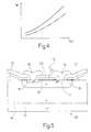
- Figure 7 shows a cross section of the chip 20 incorporating the JFET transistor 23.
- the JFET transistor 23 comprises a gate region 24 housed in a well 25 formed in the epitaxial layer 14. A portion 32 of the well 25 located beneath the gate region 24 forms the channel region of the JFET transistor 23. When a potential is applied to the gate region 24, it modulates the channel region 32.
- the gate region 24 is in electrical contact via a gate metallization region 26 which, in turn, is connected to the control terminal of the JFET transistor 23 ( Figure 3).
- the well 25 is in electrical contact via a drain metallization region 27 and a source metallization region 28 which are set on opposite sides of the gate metallization region 26 and are, in turn, connected, respectively, to the first conduction terminal and to the second conduction terminal of the JFET transistor 23 ( Figure 3).
- An insulating dielectric 33 covers portions 34 of the well 25 and of the gate region 24 which are not in electrical contact with the metallization regions 26, 27, 28, insulating the former from the latter.
- Thick field-oxide portions 35 set at the sides of the well 25, protect the edges of the JFET transistor 23.
- electrical access to the chip 20 is via the gate terminal 2, source terminal 3, and drain terminal 4 of the power device 1 ( Figure 3).
- a voltage V gs (voltage present between the gate terminal 2 and source terminal 3 of the power device 1) of a value such as to cause pinch-off of the JFET transistor 23.
- the JFET transistor 23 behaves like a resistor with a resistance r gs having a sufficiently high value (pinched resistor).
- the power device 1 described herein affords the advantages illustrated in what follows.
- the power device 1 is protected, by means of the protection circuit 11, against undesirable self-activation.
- the power device 1 can operate correctly, in that the protection circuit 11, in normal operating conditions, behaves like an open circuit with respect to the charge supplied to the gate terminal 2 by the control unit 10.
- circuit application in which the power device according to the invention is employed affords considerable advantages in terms of safety and in terms of reliability, these being extremely important factors if the device is used for automotive applications.
- the protection circuit 11 is easy to construct and can be integrated using the same techniques as those used for integrating the power device 1, so keeping the fabrication costs low.
- MOS transistor 12 or the JFET transistor 23 may be replaced, for example, by a bipolar-type transistor.
Landscapes
- Semiconductor Integrated Circuits (AREA)
- Metal-Oxide And Bipolar Metal-Oxide Semiconductor Integrated Circuits (AREA)
- Electronic Switches (AREA)
Abstract

Description
- Figure 1 presents a circuit diagram of a known power device;
- Figure 2 presents the circuit diagram of a first embodiment of a power device according to the invention;
- Figure 3 presents the circuit diagram of a second embodiment of a power device according to the invention;
- Figure 4 shows the plot of an electrical quantity taken on the power device of Figure 3;
- Figures 5 and 6 show cross sections through a chip incorporating a portion of the power device of Figure 2; and
- Figure 7 shows a cross section through a chip incorporating a portion of the power device of Figure 3.
Claims (8)
- A MOS-type power device (1) having a first conduction terminal (4) and a second conduction terminal (3), and a control terminal (2), characterized in that it comprises a variable-resistance protection circuit (11) having a first conduction terminal and a second conduction terminal connected, respectively, to said control terminal (2) and to said second conduction terminal (3) of said power device (1), said protection circuit (11) having a resistance variable between a first value and a second value according to an operating condition of said power device.
- The device according to Claim 1, characterized in that said protection circuit (11) comprises switching means (12; 23).
- The device according to Claim 2, characterized in that switching means comprise an ON-OFF switch (12).
- The device according to Claim 3, characterized in that said ON-OFF switch comprises a MOS transistor (12) of the horizontal type, having a first conduction terminal and a second conduction terminal which are connected, respectively, to said first conduction terminal and second conduction terminal of said protection circuit (11), and a control terminal connected to said first conduction terminal (4) of said power device (1).
- The device according to Claim 4, characterized in that said horizontal MOS transistor is an N-channel transistor.
- The device according to Claim 2, characterized in that said switching means comprise a gradual-intervention switch (23).
- The device according to Claim 5, characterized in that said gradual-intervention switch comprises a JFET transistor (23) having a first conduction terminal and a second conduction terminal which are connected, respectively, to said first conduction terminal and second conduction terminal of said protection circuit (11), and a control terminal connected to said control terminal (2) of said power device (1).
- The device according to Claims 6, characterized in that said JFET transistor is a P-channel transistor.
Priority Applications (3)
| Application Number | Priority Date | Filing Date | Title |
|---|---|---|---|
| DE60042392T DE60042392D1 (en) | 2000-01-20 | 2000-01-20 | Power device with protection against unwanted self-activation |
| EP00830028A EP1119104B1 (en) | 2000-01-20 | 2000-01-20 | Power device with protection against undesirable self-activation |
| US09/759,599 US6518815B2 (en) | 2000-01-20 | 2001-01-11 | Power device with protection against undesirable self-activation |
Applications Claiming Priority (1)
| Application Number | Priority Date | Filing Date | Title |
|---|---|---|---|
| EP00830028A EP1119104B1 (en) | 2000-01-20 | 2000-01-20 | Power device with protection against undesirable self-activation |
Publications (2)
| Publication Number | Publication Date |
|---|---|
| EP1119104A1 true EP1119104A1 (en) | 2001-07-25 |
| EP1119104B1 EP1119104B1 (en) | 2009-06-17 |
Family
ID=8175135
Family Applications (1)
| Application Number | Title | Priority Date | Filing Date |
|---|---|---|---|
| EP00830028A Expired - Lifetime EP1119104B1 (en) | 2000-01-20 | 2000-01-20 | Power device with protection against undesirable self-activation |
Country Status (3)
| Country | Link |
|---|---|
| US (1) | US6518815B2 (en) |
| EP (1) | EP1119104B1 (en) |
| DE (1) | DE60042392D1 (en) |
Cited By (1)
| Publication number | Priority date | Publication date | Assignee | Title |
|---|---|---|---|---|
| CN104639134A (en) * | 2013-11-11 | 2015-05-20 | 三星电机株式会社 | RF switch |
Families Citing this family (10)
| Publication number | Priority date | Publication date | Assignee | Title |
|---|---|---|---|---|
| JP4037029B2 (en) * | 2000-02-21 | 2008-01-23 | 株式会社ルネサステクノロジ | Semiconductor integrated circuit device |
| DE10120524B4 (en) * | 2001-04-26 | 2015-08-20 | Infineon Technologies Ag | Device for determining the current through a power semiconductor device |
| JP2005108980A (en) * | 2003-09-29 | 2005-04-21 | Rohm Co Ltd | Semiconductor device |
| US7221195B2 (en) * | 2005-03-18 | 2007-05-22 | Alpha & Omega Semiconductor, Ltd. | MOSFET for synchronous rectification |
| US7511357B2 (en) * | 2007-04-20 | 2009-03-31 | Force-Mos Technology Corporation | Trenched MOSFETs with improved gate-drain (GD) clamp diodes |
| JP5532538B2 (en) * | 2008-02-04 | 2014-06-25 | 三菱電機株式会社 | Protection circuit |
| US8164162B2 (en) * | 2009-06-11 | 2012-04-24 | Force Mos Technology Co., Ltd. | Power semiconductor devices integrated with clamp diodes sharing same gate metal pad |
| US9143092B2 (en) * | 2011-12-14 | 2015-09-22 | Maxim Integrated Products, Inc. | Fully capacitive coupled input choppers |
| DE102013205805B4 (en) * | 2012-11-06 | 2025-08-07 | Rohde & Schwarz GmbH & Co. Kommanditgesellschaft | Limiter for broadband high-frequency signals |
| US20240421810A1 (en) * | 2023-06-19 | 2024-12-19 | Texas Instruments Incorporated | Adaptive ringing clamp |
Citations (3)
| Publication number | Priority date | Publication date | Assignee | Title |
|---|---|---|---|---|
| US4492883A (en) * | 1982-06-21 | 1985-01-08 | Eaton Corporation | Unpowered fast gate turn-off FET |
| EP0602708A2 (en) * | 1992-12-14 | 1994-06-22 | Koninklijke Philips Electronics N.V. | Control electrode disable circuit for power transistor |
| EP0703664A2 (en) * | 1994-09-20 | 1996-03-27 | Hitachi, Ltd. | Semiconductor circuit comprising means for malfunction prevention, and its use, particularly for inverters |
Family Cites Families (7)
| Publication number | Priority date | Publication date | Assignee | Title |
|---|---|---|---|---|
| US3562547A (en) * | 1967-04-17 | 1971-02-09 | Ibm | Protection diode for integrated circuit |
| US4493000A (en) * | 1983-09-30 | 1985-01-08 | Magnetic Peripherals Incorporated | Power on/off protect circuit |
| US4855620A (en) * | 1987-11-18 | 1989-08-08 | Texas Instruments Incorporated | Output buffer with improved ESD protection |
| US4875130A (en) * | 1988-07-06 | 1989-10-17 | National Semiconductor Corporation | ESD low resistance input structure |
| JPH02280621A (en) * | 1989-03-16 | 1990-11-16 | Siemens Ag | Transistor circuit |
| US5521789A (en) * | 1994-03-15 | 1996-05-28 | National Semiconductor Corporation | BICMOS electrostatic discharge protection circuit |
| US5717560A (en) * | 1996-08-23 | 1998-02-10 | Intel Corporation | ESD protection device using static capacitance coupling between drain and gate |
-
2000
- 2000-01-20 DE DE60042392T patent/DE60042392D1/en not_active Expired - Lifetime
- 2000-01-20 EP EP00830028A patent/EP1119104B1/en not_active Expired - Lifetime
-
2001
- 2001-01-11 US US09/759,599 patent/US6518815B2/en not_active Expired - Lifetime
Patent Citations (3)
| Publication number | Priority date | Publication date | Assignee | Title |
|---|---|---|---|---|
| US4492883A (en) * | 1982-06-21 | 1985-01-08 | Eaton Corporation | Unpowered fast gate turn-off FET |
| EP0602708A2 (en) * | 1992-12-14 | 1994-06-22 | Koninklijke Philips Electronics N.V. | Control electrode disable circuit for power transistor |
| EP0703664A2 (en) * | 1994-09-20 | 1996-03-27 | Hitachi, Ltd. | Semiconductor circuit comprising means for malfunction prevention, and its use, particularly for inverters |
Cited By (2)
| Publication number | Priority date | Publication date | Assignee | Title |
|---|---|---|---|---|
| CN104639134A (en) * | 2013-11-11 | 2015-05-20 | 三星电机株式会社 | RF switch |
| CN104639134B (en) * | 2013-11-11 | 2018-10-09 | 三星电机株式会社 | RF is switched |
Also Published As
| Publication number | Publication date |
|---|---|
| US6518815B2 (en) | 2003-02-11 |
| DE60042392D1 (en) | 2009-07-30 |
| US20010022525A1 (en) | 2001-09-20 |
| EP1119104B1 (en) | 2009-06-17 |
Similar Documents
| Publication | Publication Date | Title |
|---|---|---|
| US5780905A (en) | Asymmetrical, bidirectional triggering ESD structure | |
| JP5274824B2 (en) | Power supply control circuit | |
| EP0936674B1 (en) | Integrated circuit comprising a VDMOS transistor protected against overvoltages between source and gate | |
| US6072682A (en) | Protection circuit for an electric supply line in a semiconductor integrated device | |
| US5925922A (en) | Depletion controlled isolation stage | |
| CN107527904A (en) | Conductor integrated circuit device | |
| US6878996B2 (en) | MOS power transistor | |
| EP0744098B1 (en) | A protected switch | |
| KR0174235B1 (en) | Input protection circuit having load resistor using p-channel mis transistor | |
| KR101418396B1 (en) | Power semiconductor device | |
| US6518815B2 (en) | Power device with protection against undesirable self-activation | |
| US20020186518A1 (en) | Overvoltage protection circuit | |
| US5903034A (en) | Semiconductor circuit device having an insulated gate type transistor | |
| JP2002517116A (en) | Smart power element | |
| US5466952A (en) | Semiconductor device having an IGET and a control or protection component | |
| US6201677B1 (en) | Insulated gate type semiconductor apparatus with a control circuit | |
| US20030043517A1 (en) | Electro-static discharge protecting circuit | |
| US4893212A (en) | Protection of power integrated circuits against load voltage surges | |
| US6556400B1 (en) | Reverse polarity protection circuit | |
| JP3698323B2 (en) | Power switch circuit | |
| JPH0553074B2 (en) | ||
| KR940018964A (en) | Semiconductor devices | |
| EP4429110A1 (en) | High voltage semiconductor device with data transmission from a high voltage domain to a low voltage domain | |
| US11228309B2 (en) | Circuit apparatus and method for operating a circuit apparatus | |
| JPH04321773A (en) | Power integrated circuit for automobile |
Legal Events
| Date | Code | Title | Description |
|---|---|---|---|
| PUAI | Public reference made under article 153(3) epc to a published international application that has entered the european phase |
Free format text: ORIGINAL CODE: 0009012 |
|
| AK | Designated contracting states |
Kind code of ref document: A1 Designated state(s): DE FR GB IT |
|
| AX | Request for extension of the european patent |
Free format text: AL;LT;LV;MK;RO;SI |
|
| 17P | Request for examination filed |
Effective date: 20020116 |
|
| AKX | Designation fees paid |
Free format text: DE FR GB IT |
|
| 17Q | First examination report despatched |
Effective date: 20060713 |
|
| 17Q | First examination report despatched |
Effective date: 20060713 |
|
| 17Q | First examination report despatched |
Effective date: 20060713 |
|
| GRAP | Despatch of communication of intention to grant a patent |
Free format text: ORIGINAL CODE: EPIDOSNIGR1 |
|
| GRAS | Grant fee paid |
Free format text: ORIGINAL CODE: EPIDOSNIGR3 |
|
| GRAA | (expected) grant |
Free format text: ORIGINAL CODE: 0009210 |
|
| AK | Designated contracting states |
Kind code of ref document: B1 Designated state(s): DE FR GB IT |
|
| REG | Reference to a national code |
Ref country code: GB Ref legal event code: FG4D |
|
| REF | Corresponds to: |
Ref document number: 60042392 Country of ref document: DE Date of ref document: 20090730 Kind code of ref document: P |
|
| RAP2 | Party data changed (patent owner data changed or rights of a patent transferred) |
Owner name: STMICROELECTRONICS SRL |
|
| PLBE | No opposition filed within time limit |
Free format text: ORIGINAL CODE: 0009261 |
|
| STAA | Information on the status of an ep patent application or granted ep patent |
Free format text: STATUS: NO OPPOSITION FILED WITHIN TIME LIMIT |
|
| 26N | No opposition filed |
Effective date: 20100318 |
|
| GBPC | Gb: european patent ceased through non-payment of renewal fee |
Effective date: 20100120 |
|
| PG25 | Lapsed in a contracting state [announced via postgrant information from national office to epo] |
Ref country code: GB Free format text: LAPSE BECAUSE OF NON-PAYMENT OF DUE FEES Effective date: 20100120 |
|
| PGFP | Annual fee paid to national office [announced via postgrant information from national office to epo] |
Ref country code: FR Payment date: 20120216 Year of fee payment: 13 |
|
| PG25 | Lapsed in a contracting state [announced via postgrant information from national office to epo] |
Ref country code: IT Free format text: LAPSE BECAUSE OF NON-PAYMENT OF DUE FEES Effective date: 20120120 |
|
| PGFP | Annual fee paid to national office [announced via postgrant information from national office to epo] |
Ref country code: DE Payment date: 20121226 Year of fee payment: 14 |
|
| REG | Reference to a national code |
Ref country code: FR Ref legal event code: ST Effective date: 20130930 |
|
| PG25 | Lapsed in a contracting state [announced via postgrant information from national office to epo] |
Ref country code: FR Free format text: LAPSE BECAUSE OF NON-PAYMENT OF DUE FEES Effective date: 20130131 |
|
| PGFP | Annual fee paid to national office [announced via postgrant information from national office to epo] |
Ref country code: IT Payment date: 20111222 Year of fee payment: 13 |
|
| PGRI | Patent reinstated in contracting state [announced from national office to epo] |
Ref country code: IT Effective date: 20131025 |
|
| REG | Reference to a national code |
Ref country code: DE Ref legal event code: R119 Ref document number: 60042392 Country of ref document: DE |
|
| REG | Reference to a national code |
Ref country code: DE Ref legal event code: R119 Ref document number: 60042392 Country of ref document: DE Effective date: 20140801 |
|
| PG25 | Lapsed in a contracting state [announced via postgrant information from national office to epo] |
Ref country code: DE Free format text: LAPSE BECAUSE OF NON-PAYMENT OF DUE FEES Effective date: 20140801 |
|
| PGRI | Patent reinstated in contracting state [announced from national office to epo] |
Ref country code: IT Effective date: 20131025 |