EP1119045A2 - Diamond interconnection substrate and a manufacturing method therefor - Google Patents
Diamond interconnection substrate and a manufacturing method therefor Download PDFInfo
- Publication number
- EP1119045A2 EP1119045A2 EP01300474A EP01300474A EP1119045A2 EP 1119045 A2 EP1119045 A2 EP 1119045A2 EP 01300474 A EP01300474 A EP 01300474A EP 01300474 A EP01300474 A EP 01300474A EP 1119045 A2 EP1119045 A2 EP 1119045A2
- Authority
- EP
- European Patent Office
- Prior art keywords
- diamond
- metal elements
- interconnection substrate
- layer
- implantation
- Prior art date
- Legal status (The legal status is an assumption and is not a legal conclusion. Google has not performed a legal analysis and makes no representation as to the accuracy of the status listed.)
- Granted
Links
Images








Classifications
-
- H—ELECTRICITY
- H10—SEMICONDUCTOR DEVICES; ELECTRIC SOLID-STATE DEVICES NOT OTHERWISE PROVIDED FOR
- H10W—GENERIC PACKAGES, INTERCONNECTIONS, CONNECTORS OR OTHER CONSTRUCTIONAL DETAILS OF DEVICES COVERED BY CLASS H10
- H10W40/00—Arrangements for thermal protection or thermal control
- H10W40/20—Arrangements for cooling
- H10W40/25—Arrangements for cooling characterised by their materials
- H10W40/254—Diamond
-
- H—ELECTRICITY
- H10—SEMICONDUCTOR DEVICES; ELECTRIC SOLID-STATE DEVICES NOT OTHERWISE PROVIDED FOR
- H10W—GENERIC PACKAGES, INTERCONNECTIONS, CONNECTORS OR OTHER CONSTRUCTIONAL DETAILS OF DEVICES COVERED BY CLASS H10
- H10W70/00—Package substrates; Interposers; Redistribution layers [RDL]
- H10W70/01—Manufacture or treatment
- H10W70/05—Manufacture or treatment of insulating or insulated package substrates, or of interposers, or of redistribution layers
-
- H—ELECTRICITY
- H10—SEMICONDUCTOR DEVICES; ELECTRIC SOLID-STATE DEVICES NOT OTHERWISE PROVIDED FOR
- H10W—GENERIC PACKAGES, INTERCONNECTIONS, CONNECTORS OR OTHER CONSTRUCTIONAL DETAILS OF DEVICES COVERED BY CLASS H10
- H10W70/00—Package substrates; Interposers; Redistribution layers [RDL]
- H10W70/60—Insulating or insulated package substrates; Interposers; Redistribution layers
- H10W70/67—Insulating or insulated package substrates; Interposers; Redistribution layers characterised by their insulating layers or insulating parts
- H10W70/69—Insulating materials thereof
-
- H—ELECTRICITY
- H05—ELECTRIC TECHNIQUES NOT OTHERWISE PROVIDED FOR
- H05K—PRINTED CIRCUITS; CASINGS OR CONSTRUCTIONAL DETAILS OF ELECTRIC APPARATUS; MANUFACTURE OF ASSEMBLAGES OF ELECTRICAL COMPONENTS
- H05K3/00—Apparatus or processes for manufacturing printed circuits
- H05K3/10—Apparatus or processes for manufacturing printed circuits in which conductive material is applied to the insulating support in such a manner as to form the desired conductive pattern
- H05K3/14—Apparatus or processes for manufacturing printed circuits in which conductive material is applied to the insulating support in such a manner as to form the desired conductive pattern using spraying techniques to apply the conductive material, e.g. vapour evaporation
Definitions
- the present invention relates to a diamond interconnection substrate and a manufacturing method therefor, and more particularly to those applicable to a high-power electronic circuit substrate including a high power microwave circuit, which is a diamond circuit substrate, also serving as a heat sink, having multi-layer interconnections.
- Diamond is a material having the highest thermal conductivity of all materials, in a high temperature range between a room temperature and 200 °C. Such a property is considered to be important for a heat sink required for lowering temperature of electron devices having, year by year, higher performance and greater heat-releasing values.
- diamond when utilized as a high-performance heat sink, diamond may be provided with an interconnection of only one layer formed on the surface of the diamond. Thus, a conventional diamond interconnection substrate has attained only one layer of interconnection.
- the interconnections may cross with each other in the only one interconnection layer. Further, miniaturization of a device may possibly make an interconnection thinner, which will require the interconnection to be electrical power resistant.
- circuit substrates are used for circuit substrates, and a combination of simultaneously calcinable Al 2 O 3 /W, AlN/W or the like are selected as materials therefor.
- Some circuit substrates are designed to utilize CuW material, a low-temperature calcinated substrate and so forth, to be divided into a heat radiating portion and a multi-layer interconnection portion.
- a multi-layer interconnection substrate of BeO is being contemplated in a field where both a highly thermal conductive material and a multi-layer interconnection technique are required.
- a diamond interconnection substrate includes diamond, and a conductive layer constituted by a presence of metal elements having a thickness of at least 10 nm and a concentration of at least 10 20 cm -3 in the diamond. More effectively, the conductive layer is constituted by the presence of metal elements having a thickness of at least 100 nm and a concentration of at least 10 21 cm -3 .
- the diamond interconnection substrate of the present invention utilizes diamond having a thermal conductivity of approximately 2000 W/mK for the substrate, in which interconnections are provided within the diamond by implanting metal ions into the diamond substrate with a high energy level and a high dose.
- Diamond is constituted by carbon atoms, each of which being a light element, and, different from Si and so forth, ions can enter very deeply into the diamond when implanted at a high speed.
- fast ions on the order of MeV
- the scattering cross section is increased and the ions are rapidly stalled once the ions are decelerated in a substance, so that concentrated implantation is possible in a very narrow region.
- interconnections that are patterned together. That is, the interconnections can be formed with excellent controllability in depth and plane directions. It is also possible to attain a density value in the diamond very close to a density of metal, with a practical implant dose. This means that transfer of another substance into the diamond is possible rather than simple doping of elements.
- the diamond may be monocrystal or polycrystal, and either will have almost the same effect. Further, the effect described above can be attained even if an impurity is mixed in the diamond, since no doping is performed.
- interconnections are provided within the diamond, so that no gap can be formed between the diamond and the interconnections, and thus the interconnections cannot be corroded nor oxidized by acid or a severe environmental atmosphere.
- corrosive metals of alkali metals or alkaline earth metals may be utilized for the interconnections. It is understood that refractory metals of W, Mo, Nb, Pt and Ir may also be used. Lighter elements such as Li and Na of the metal elements can be implanted deeper, thereby causing less damage to the diamond.
- a property in that the substrate has a high thermal conductivity allows heat of the interconnection to be dissipated, so that even a low melting material can have electrical power resistance.
- the diamond interconnection substrate includes a plurality of conductive layers, the plurality of conductive layers being disposed at different depth positions with various distances from a surface of the diamond.
- the plurality of conductive layers are electrically connected with each other in the diamond.
- each conductive layer to be electrically connected with each other.
- the diamond interconnection substrate further includes at least one electrode formed on the surface of the diamond, and at least one of the plurality of conductive layers is electrically connected to the at least one electrode.
- the metal elements constituting the conductive layer are metal elements of at least one species selected from a group consisting of Cu, Ag, Au, Pt, Mg and Al.
- a material can be selected as appropriate, and a low-melting/low-resistant material can be used to form the interconnections.
- a method of manufacturing a diamond interconnection substrate according to the present invention includes the step of ion implanting metal elements with energy of at least 1 MeV and a dose of at least 10 16 cm -2 into diamond to form a conductive layer constituted by the metal elements.
- the conductive layers that are to be interconnections can be formed within the diamond as described above, by ion implantation with the high energy (at least 1 MeV) and the high dose (at least 10 16 cm -2 ).
- the ion implanting is performed a number of times by varying implantation depths of the metal elements into the diamond.
- Implantation at different implantation depths can provide various arrangement positions and shapes of the conductive layers.
- the implantation depth can be changed by varying implantation energy. For example, if Cu ions are implanted with various energy levels such as 8 MeV, 6 MeV and 4 MeV, profiles of Cu ions implanted in respective implantation processes are partly overlapped with each other and are stacked in the depth direction.
- the implantation depth can be varied even with a constant energy, by disposing an interposition somewhere in an ion implantation path.
- an interposition somewhere in an ion implantation path.
- the metal layers serve as decelerating layers for the implanted ions, which effectively varies the energy level of the implanted ions in the diamond, resulting in various implantation depths. This allows the profiles of Cu ions implanted in respective stages to be partly overlapped with each other and stacked in the depth direction.
- the implantation depth can also be varied by changing ion species to be implanted, even with the same energy level.
- ion species For example, when Al ions are implanted with 5 MeV and Cu is implanted with 8 MeV, the respective profiles of Al ions and Cu ions are overlapped with each other. When the implantation profiles are thus overlapped, a width of the implantation region in the depth direction will be thicker compared to that of a single implantation profile alone, and further a resistance value of the implantation region will be lowered. Thus, implantation can control the thickness of the conductive layers.
- profiles of the metal elements implanted by the number of times of the ion implanting are overlapped with each other while being stacked in a depth direction to form a single conductive layer.
- profiles of the metal elements implanted by the number of times of the ion implanting are disposed at different depth positions without overlapping with each other, to form a plurality of conductive layers divided in multiple layers.
- profiles will not be overlapped when energy levels of 8 MeV and 2 MeV are used to implant Cu, or when 6 MeV is used to implant Al and 4 MeV is used to implant Cu.
- implantation depth can be controlled.
- a method in which at least 1 ⁇ m of diamond is formed on an implantation surface by a vapor synthesizing process after one implantation step and thereafter a further implantation step is performed can be used to form profiles without an overlap (even when the implantation is performed under the same condition).
- multi-layer interconnections having arbitrary shapes can also be performed by using masks having different patterns for the respective implantation steps.
- fabricating a multi-layer interconnection substrate having an interconnection of an arbitrary shape at an arbitrary interlayer is enabled. Further, the method of controlling the thickness of the conductive layers described earlier can be used to form conductive layers having arbitrary thicknesses at arbitrary layers.
- the conductive layers can have the thickness ranging from a predetermined depth position to the surface. This method can be utilized for extracting an electrode to the top surface and for forming an electrode connecting between layers.
- At least one of implanting energy of the ion implanting and species of the metal elements is changed to vary an implantation depth of the metal elements in the ion implanting.
- the method of manufacturing a diamond interconnection substrate further includes the step of synthesizing a diamond layer on a surface of the diamond by a vapor synthesizing process, and the step of ion implanting the metal elements and the step of synthesizing the diamond layer after the ion implanting are repeated to form multi-layered conductive layer disposed on planes different from each other.
- the present invention allows synthesis of diamond at approximately 1000 °C over the substrate after provision of the interconnections.
- the total number of the multi-layer interconnections can almost be infinity, and a low melting/low resistivity material (Al, Ag, Au and Mg) can be used for the interconnection metal.
- a mask layer formed on a surface of the diamond is patterned using a photolithography process, and the ion implanting is performed to the diamond through the patterned mask layer, to form the conductive layer of a predetermined shape.
- a diamond interconnection substrate 10 includes a diamond substrate 1 and conductive layers 2, 3 and 4.
- Conductive layers 2, 3 and 4 are formed in diamond substrate 1, and are constituted by the presence of metal elements having a thickness of at least 10 nm and a concentration of at least 10 20 cm -3 .
- thickness T 1 of conductive layer 2, a thickness T 2 of conductive layer 3 and a thickness of conductive layer 4 are all at least 10 nm.
- the metal elements of each conductive layer 2, 3 and 4 preferably have a concentration of equal to or less than 10 22 cm -3 .
- conductive layers 2, 3 and 4 for example, low-melting/low-resistive Al, Ag, Au, Mg and Cu may be used, or refractory metals such as W, Mo, Nb, Pt and Ir may be used, or corrosive alkali metals or alkaline earth metals may also be used.
- Conductive layers may be formed on different planes (in different depth positions) as multi-layer interconnections, such as conductive layers 2 and 3. Furthermore, these conductive layers 2 and 3 may be electrically connected with each other by a layer having a long width (thickness) in the depth direction such as conductive layer 4. This conductive layer 4 may also reach the surface of diamond substrate 1 and may electrically contact with an electrode 5 formed on the surface.
- Conductive layer 4 may be formed by conductive regions 4a, each formed in an ion implantation step, stacked in the depth direction while sharing overlapped regions 4b, as shown in the sectional view of Fig. 2. It can also be formed simply from a single metal layer filled in a via hole opened through the surface of diamond substrate 1.
- Diamond substrate 1 may be a natural diamond substrate, an artificial (high-pressure synthetic) diamond substrate, a vapor synthesized diamond substrate, a polycrystalline diamond substrate, an alignment-controlled polycrystalline diamond substrate, a hetero-epitaxial substrate, or a monocrystal diamond substrate.
- the hetero-epitaxial substrate and the monocrystal substrate are required such that no channeling occurs at the time of implantation.
- the polycrystalline substrate an uneven surface is not preferable because the unevenness would be reflected to conductive layers 2 and 3 constituted by metal elements implanted from the surface.
- a monocrystal substrate, a hetero-epitaxial substrate, an alignment-controlled flat polycrystalline substrate, or a flatly polished polycrystalline substrate is used.
- the method of forming the diamond may either be
- a mask 11 having, for example, a linear opening pattern 11a is formed or disposed on the surface of diamond substrate 1.
- metal elements are ion implanted with implanting energy of at least 1 MeV and a dose of at least 10 16 cm -2 .
- a mask 12 having, for example, a linear opening pattern 12a is formed or disposed on the surface of diamond substrate 1.
- metal elements are ion implanted with energy of at least 1 MeV and a dose of at least 10 16 cm -2 .
- a mask 13 having a predetermined opening pattern 13a is formed or disposed on the surface of diamond substrate 1.
- metal elements are ion implanted to diamond substrate 1 a number of times with a dose of at least 10 16 cm -2 and at various implantation depths.
- a plurality of conductive regions 4a having different implantation depths are formed to be overlapped with each other as shown in Fig. 2, resulting in conductive layer 4 which electrically connects conductive layers 2 and 3 while reaching the surface of diamond substrate 1.
- the implantation depth of the metal elements may be varied by changing a level of ion implanting energy, by changing species of metal elements, or by interposing some layer in the implantation path of the metal elements.
- photolithography and etching processes may be used to form a via hole in diamond substrate 1, and then metal or the like may be embedded into the via hole to form a single conductive layer 4.
- Mask layers 11, 12 and 13 may also be formed to have opening patterns 11a, 12a and 13a formed by the photolithography process, and may also be metal masks disposed with a distance from the surface of diamond substrate 1.
- the diamond interconnection substrate according to the present embodiment may be used for a semiconductor device utilized with high power, for example, for a high-power laser diode for optical amplification of a communication system, as a circuit substrate for microwave output of a communication satellite, and for a power module for controlling high electric power.
- Ion implantation was performed to a monocrystal or polycrystalline diamond substrate 101 with energy of the order of MeV through a metal mask 111a having a pattern shown in Fig. 6.
- an implantation region (conductive layer) 102 with a pattern similar to that of metal mask 111a was formed.
- the implantation region 102 could also be formed by implanting ions with energy of the order of MeV through a patterned mask material 111b as shown in Fig. 7, rather than using metal mask 111a.
- implantation region 102 was formed directly below a region where no mask materials exist. Though the film thickness of mask materials 111a and 111b is different depending on their materials and the level of implanting energy, at least 10 ⁇ m is required.
- a measurement method 1 evaluation was made for a resistance value of implantation region 102, determined by a ratio of flowing current I1 to a measured voltage V1 when a voltage is applied to both ends of implantation region 102 as shown in Fig. 8. Further, in measurement method 2, evaluation was made for a resistance value determined by a current-voltage property between implantation region 102 and a surface electrode 105, as shown in Figs. 9 and 10. It is noted that Fig. 10 is a sectional view of Fig. 9.
- the depth of the implantation region is at least 0.5 ⁇ m.
- a metal mask or a mask 113 to which a mask material had been patterned was disposed or formed on diamond substrate 101, and thereafter ions were implanted with a predetermined implanting energy level through mask 113. As a result, an implantation region 104a was formed at a predetermined depth in diamond substrate 101.
- implantation was performed at different energy levels at intervals (such as 8 MeV, 6 MeV, 4 MeV, 2 MeV, 0.4 MeV, 100 keV and 40 keV), such that profiles of implantation regions are overlapped with each other from a high energy (8 MeV) to a low energy ( ⁇ 40 keV) as shown in Figs. 12A and 12B. It was found that energy variation changes implantation depths (thickness of the implantation layer) and decreases the resistance value to a surface layer, resulting in conduction to the surface. Conductive connection to the surface realized a resistance equal to or less than 10 ⁇ . This was determined from the results in Tables 1 to 3, considering the fact that these results were obtained through contact resistance.
- Implantation region 104 formed as such was applied for four pad portions in Fig. 8 and a pad portion to which V2 contacts in Fig. 9.
- a mask 111 having a linear opening pattern 111a was disposed or formed on diamond substrate 101, and thereafter ions were implanted with high energy (8 MeV) through the mask 111 to form an implantation region 102 of metal elements. Subsequently, as shown in Figs. 14A and 14B, ions were implanted with low energy (2 MeV) through a mask 112 having an opening pattern extending in a direction orthogonal to implantation region 102. Thus, an implantation region 103 of metal elements was formed at a position shallower than implantation region 102.
- the opening pattern of mask 112 is positioned directly above implantation region 103.
- a profile of atoms in the depth direction was examined by SIMS (Secondary Ion Mass Spectrometry) for the obtained diamond interconnection substrate, to find a separated profile having two peaks.
- a resistance value between implantation regions 102 and 103 was examined to find a large value equal to or higher than 10 k ⁇ .
- interlayer resistance value By annealing in hydrogen plasma at 800 to 1000 °C, interlayer resistance value showed a tendency to be increased by at least approximately one order. This showed that an implantation region of a multi-layer structure having a high interlayer resistance value could be formed.
- multi-layer structured implantation regions 102 and 103 as shown in Figs. 14A and 14B were formed with high energy (8 MeV) and lower energy (2 MeV) by a method similar to that of Example 4. Subsequently, ion implantation was performed a number of times, with different implant energy levels of 8, 6, 4 and 2 MeV, to a crossing portion of implantation regions 102 and 103. Thus, a plurality of implant layers 104a were formed for electrically connecting implantation regions 102 and 103. Thus, it was observed that the interlayer electrical resistance decreases from a large value equal to or more than 10 k ⁇ to a small value equal to or less than 10 ⁇ .
- the implanting energy was made constant to be 8 MeV and a thin film 121 was placed before the implantation surface.
- the energy with which ions are implanted into diamond substrate 101 may be varied almost continuously. This also made it possible to obtain a small value of interlayer electric resistance equal to or less than 5 ⁇ .
- An implantation region was formed between layers and on the top surface by a method similar to that of Example 5 in combination with the method of Example 3, to form a contact layer 104 shared by implantation regions 102 and 103 as shown in Figs. 17A and 17B.
- Contact layer 104 reaches the surface of diamond interconnection substrate 101. Further, the contact resistance value in this configuration indicated a value almost as same as that in Example 3.
- interlayer insulated implantation regions 102 and 103 were formed in diamond substrate 101 by a method similar to that of Example 4. Subsequently, a crossing portion of implantation regions 102 and 103 was etched by RIE (Reactive Ion Etching) or ion beam etching processes until the portion reaches implantation region 102. The resulted hole was embedded with metal having a melting point of 500 °C or lower to form an electrode 104. Because of a poor wetting property of low melting metal to diamond, Ti may be deposited in the hole to increase adhesion of metal therein, which otherwise is low, resulting in an optimal electrode isolation.
- RIE Reactive Ion Etching
- ion beam etching processes until the portion reaches implantation region 102.
- the resulted hole was embedded with metal having a melting point of 500 °C or lower to form an electrode 104. Because of a poor wetting property of low melting metal to diamond, Ti may be deposited in the hole to increase adhesion of metal therein, which otherwise is low,
- an implantation region 102 having an appropriate pattern was formed by implanting Cu ions into diamond substrate 101 with energy of 8 MeV, as in the case with Example 1. Subsequently, non-doped diamond layer 131 having a thickness of at least 0.3 ⁇ m was formed on diamond substrate 101 by a vapor synthesizing method, as shown in Figs. 20A and 20B. Thereafter, an implantation region 103 having another pattern was formed by implanting Cu ions with implanting energy of 2 MeV, as shown in Figs. 21A and 21B. It is noted that, in Figs. 21A and 21B, an opening pattern of mask 112 is positioned directly above implantation region 103.
- interlayer insulation resistance was increased.
- diamond layer 131 was formed having a thickness of at least 3 ⁇ m, interlayer insulation was secured even though the same ion implanting energy of 8 MeV was used for the second implantation. It was also possible to stack more than two layers, i.e. three, four or more layers.
- diamond having the highest thermal conductivity of all materials can be provided with multi-layer interconnections, to attain a substrate suitable for a high-power electronic circuit substrate including a high-power microwave circuit.
Landscapes
- Crystals, And After-Treatments Of Crystals (AREA)
- Internal Circuitry In Semiconductor Integrated Circuit Devices (AREA)
- Manufacturing Of Printed Wiring (AREA)
Abstract
Description
- The present invention relates to a diamond interconnection substrate and a manufacturing method therefor, and more particularly to those applicable to a high-power electronic circuit substrate including a high power microwave circuit, which is a diamond circuit substrate, also serving as a heat sink, having multi-layer interconnections.
- Diamond is a material having the highest thermal conductivity of all materials, in a high temperature range between a room temperature and 200 °C. Such a property is considered to be important for a heat sink required for lowering temperature of electron devices having, year by year, higher performance and greater heat-releasing values. Conventionally, when utilized as a high-performance heat sink, diamond may be provided with an interconnection of only one layer formed on the surface of the diamond. Thus, a conventional diamond interconnection substrate has attained only one layer of interconnection.
- However, when a number of elements are formed on the diamond substrate, the interconnections may cross with each other in the only one interconnection layer. Further, miniaturization of a device may possibly make an interconnection thinner, which will require the interconnection to be electrical power resistant.
- Currently, ceramics and conductors are used for circuit substrates, and a combination of simultaneously calcinable Al2O3/W, AlN/W or the like are selected as materials therefor. Some circuit substrates are designed to utilize CuW material, a low-temperature calcinated substrate and so forth, to be divided into a heat radiating portion and a multi-layer interconnection portion. Further, a multi-layer interconnection substrate of BeO is being contemplated in a field where both a highly thermal conductive material and a multi-layer interconnection technique are required.
- However, such a circuit substrate had problems in that the thermal conductivity is lower compared to that of diamond, its structure is more complicated and its manufacturing process is troublesome.
- It is an object of the present invention to provide a technique by which multi-layer interconnections can be realized using a diamond substrate with the highest thermal conductivity of all materials, in a packaging field for a high power microwave and milliwave communications requiring a high thermal conductivity and a multi-layer interconnection technique.
- A diamond interconnection substrate according to the present invention includes diamond, and a conductive layer constituted by a presence of metal elements having a thickness of at least 10 nm and a concentration of at least 1020 cm-3 in the diamond. More effectively, the conductive layer is constituted by the presence of metal elements having a thickness of at least 100 nm and a concentration of at least 1021 cm-3.
- To solve the problems described above, the diamond interconnection substrate of the present invention utilizes diamond having a thermal conductivity of approximately 2000 W/mK for the substrate, in which interconnections are provided within the diamond by implanting metal ions into the diamond substrate with a high energy level and a high dose.
- Diamond is constituted by carbon atoms, each of which being a light element, and, different from Si and so forth, ions can enter very deeply into the diamond when implanted at a high speed. Further, fast ions (on the order of MeV) have a property in which a scattering cross section is small as long as the ions are at the high speed, so that they hardly collide with elements in crystal, passing through the crystal without much damage thereto. However, the scattering cross section is increased and the ions are rapidly stalled once the ions are decelerated in a substance, so that concentrated implantation is possible in a very narrow region.
- Further, use of a mask enables forming of interconnections that are patterned together. That is, the interconnections can be formed with excellent controllability in depth and plane directions. It is also possible to attain a density value in the diamond very close to a density of metal, with a practical implant dose. This means that transfer of another substance into the diamond is possible rather than simple doping of elements.
- Further, in a case that a conventional substance is used as a substrate material, when ions are implanted, energy of implanted elements may locally increase temperature and pressure of the material originally constituting the substrate, which may destroy the material. On the other hand, diamond has a high thermal conductivity such that it is hard to be heated to a high temperature, and also is very strongly bonded so as not to be destroyed.
- Therefore, implantation of fast metal ions into the diamond can realize provision of interconnection within the diamond.
- The diamond may be monocrystal or polycrystal, and either will have almost the same effect. Further, the effect described above can be attained even if an impurity is mixed in the diamond, since no doping is performed.
- Further, interconnections are provided within the diamond, so that no gap can be formed between the diamond and the interconnections, and thus the interconnections cannot be corroded nor oxidized by acid or a severe environmental atmosphere. Thus, corrosive metals of alkali metals or alkaline earth metals may be utilized for the interconnections. It is understood that refractory metals of W, Mo, Nb, Pt and Ir may also be used. Lighter elements such as Li and Na of the metal elements can be implanted deeper, thereby causing less damage to the diamond.
- Further, a property in that the substrate has a high thermal conductivity allows heat of the interconnection to be dissipated, so that even a low melting material can have electrical power resistance.
- Preferably, the diamond interconnection substrate includes a plurality of conductive layers, the plurality of conductive layers being disposed at different depth positions with various distances from a surface of the diamond.
- This can realize a multi-layer interconnection structure, facilitates arrangement of interconnections, and also realizes integration.
- Preferably, in the diamond interconnection substrate, the plurality of conductive layers are electrically connected with each other in the diamond.
- This allows each conductive layer to be electrically connected with each other.
- Preferably, the diamond interconnection substrate further includes at least one electrode formed on the surface of the diamond, and at least one of the plurality of conductive layers is electrically connected to the at least one electrode.
- This enables the conductive layers to be electrically connected to the outside via the electrode.
- Preferably, in the diamond interconnection substrate, the metal elements constituting the conductive layer are metal elements of at least one species selected from a group consisting of Cu, Ag, Au, Pt, Mg and Al.
- Thus, a material can be selected as appropriate, and a low-melting/low-resistant material can be used to form the interconnections.
- A method of manufacturing a diamond interconnection substrate according to the present invention includes the step of ion implanting metal elements with energy of at least 1 MeV and a dose of at least 1016 cm-2 into diamond to form a conductive layer constituted by the metal elements.
- According to the manufacturing method of the diamond interconnection substrate of the present invention, the conductive layers that are to be interconnections can be formed within the diamond as described above, by ion implantation with the high energy (at least 1 MeV) and the high dose (at least 1016 cm-2).
- Preferably, in the method of manufacturing a diamond interconnection substrate, the ion implanting is performed a number of times by varying implantation depths of the metal elements into the diamond.
- Implantation at different implantation depths can provide various arrangement positions and shapes of the conductive layers.
- The implantation depth can be changed by varying implantation energy. For example, if Cu ions are implanted with various energy levels such as 8 MeV, 6 MeV and 4 MeV, profiles of Cu ions implanted in respective implantation processes are partly overlapped with each other and are stacked in the depth direction.
- Alternatively, the implantation depth can be varied even with a constant energy, by disposing an interposition somewhere in an ion implantation path. For example, there is a method of implanting ions in multiple stages, in which ions are first implanted with the energy level of 8 MeV without any interpolations in the implantation path, and thereafter ions are implanted with a thin (100 to 200 nm) metal layer interposed somewhere in the implantation path, and then ions are further implanted with a thicker metal layer interposed. In such a case, the metal layers serve as decelerating layers for the implanted ions, which effectively varies the energy level of the implanted ions in the diamond, resulting in various implantation depths. This allows the profiles of Cu ions implanted in respective stages to be partly overlapped with each other and stacked in the depth direction.
- Alternatively, the implantation depth can also be varied by changing ion species to be implanted, even with the same energy level. For example, when Al ions are implanted with 5 MeV and Cu is implanted with 8 MeV, the respective profiles of Al ions and Cu ions are overlapped with each other. When the implantation profiles are thus overlapped, a width of the implantation region in the depth direction will be thicker compared to that of a single implantation profile alone, and further a resistance value of the implantation region will be lowered. Thus, implantation can control the thickness of the conductive layers.
- Preferably, in the method of manufacturing a diamond interconnection substrate, profiles of the metal elements implanted by the number of times of the ion implanting are overlapped with each other while being stacked in a depth direction to form a single conductive layer.
- As described above, by changing the implantation depth for each ion implantation in a plurality of ion implantation steps, it will be possible to stack the profiles of metal elements implanted in the respective implantation steps in the depth direction.
- Preferably, in the method of manufacturing a diamond interconnection substrate, profiles of the metal elements implanted by the number of times of the ion implanting are disposed at different depth positions without overlapping with each other, to form a plurality of conductive layers divided in multiple layers.
- For example, profiles will not be overlapped when energy levels of 8 MeV and 2 MeV are used to implant Cu, or when 6 MeV is used to implant Al and 4 MeV is used to implant Cu. Thus, implantation depth can be controlled. Further, a method in which at least 1 µm of diamond is formed on an implantation surface by a vapor synthesizing process after one implantation step and thereafter a further implantation step is performed, can be used to form profiles without an overlap (even when the implantation is performed under the same condition). By repeating this once or more than once, arbitrary multi-layered conductive layers can be formed. Further, multi-layer interconnections having arbitrary shapes can also be performed by using masks having different patterns for the respective implantation steps. As such, fabrication of a multi-layer interconnection substrate having an interconnection of an arbitrary shape at an arbitrary interlayer is enabled. Further, the method of controlling the thickness of the conductive layers described earlier can be used to form conductive layers having arbitrary thicknesses at arbitrary layers.
- Moreover, if the energy level is changed in a fairly large range and implant ion species is also changed by the method of controlling the thickness of the conductive layers described earlier, the conductive layers can have the thickness ranging from a predetermined depth position to the surface. This method can be utilized for extracting an electrode to the top surface and for forming an electrode connecting between layers.
- It is noted that, not only the implantation, deposition or embedment of a metal layer into a via hole formed after formation of multi-layer interconnection also enables connection between layers and extraction of an electrode to the top surface.
- Preferably, in the method of manufacturing a diamond interconnection substrate, at least one of implanting energy of the ion implanting and species of the metal elements is changed to vary an implantation depth of the metal elements in the ion implanting.
- This enables formation of conductive layers having different widths (thickness) in the depth direction and formation of a multi-layer interconnection structure, as described above.
- Preferably, the method of manufacturing a diamond interconnection substrate further includes the step of synthesizing a diamond layer on a surface of the diamond by a vapor synthesizing process, and the step of ion implanting the metal elements and the step of synthesizing the diamond layer after the ion implanting are repeated to form multi-layered conductive layer disposed on planes different from each other.
- Through the characteristics as described above, the present invention allows synthesis of diamond at approximately 1000 °C over the substrate after provision of the interconnections. Thus, by repeating the step of ion implanting metal elements and the step of synthesizing the diamond layer, the total number of the multi-layer interconnections can almost be infinity, and a low melting/low resistivity material (Al, Ag, Au and Mg) can be used for the interconnection metal.
- Preferably, in the method of manufacturing a diamond interconnection substrate, a mask layer formed on a surface of the diamond is patterned using a photolithography process, and the ion implanting is performed to the diamond through the patterned mask layer, to form the conductive layer of a predetermined shape.
- This enables two-dimensionally controlled patterning by the mask.
- The foregoing and other objects, features, aspects and advantages of the present invention will become more apparent from the following detailed description of the present invention when taken in conjunction with the accompanying drawings, provided by way of example.
- Fig. 1 is a perspective view schematically showing a configuration of a diamond interconnection substrate according to an embodiment of the present invention;
- Fig. 2 is a partial section view schematically showing a configuration of a diamond interconnection substrate according to an embodiment of the present invention;
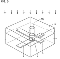
- Figs. 3 to 5 are schematic perspective views sequentially illustrating steps of a manufacturing method of a diamond interconnection substrate according to an embodiment of the present invention;
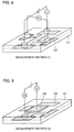
- Fig. 6 is a schematic perspective view illustrating formation of an implantation region using a metal mask;
- Fig. 7 is a schematic perspective view showing formation of an implantation region using a patterned mask material;
- Fig. 8 is a schematic perspective view for illustrating a
measurement method 1; - Fig. 9 is a schematic perspective view for illustrating a
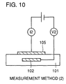
measurement method 2; - Fig. 10 is a schematic section view for illustrating the
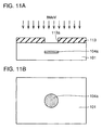
measurement method 2; - Figs. 11A, 11B, 12A and 12B are sectional and planar views sequentially showing steps of a manufacturing method of a diamond interconnection substrate according to the third embodiment of the present invention;
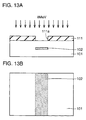
- Figs. 13A, 13B, 14A and 14B are sectional and planar views sequentially showing steps of a manufacturing method of a diamond interconnection substrate according to the fourth embodiment of the present invention;
- Figs. 15A and 15B are sectional and planar views showing a manufacturing method of a diamond interconnection substrate according to the fifth embodiment of the present invention;
- Figs. 16A and 16B are sectional and planar views showing another manufacturing method of the diamond interconnection substrate according to the fifth embodiment of the present invention;
- Figs. 17A and 17B are sectional and planar views showing a manufacturing method of a diamond interconnection substrate according to the sixth embodiment of the present invention;
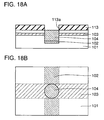
- Figs. 18A and 18B are sectional and planar views showing a manufacturing method of a diamond interconnection substrate according to the seventh embodiment of the present invention;
- Figs. 19A, 20A and 21A are sectional views sequentially showing steps of a manufacturing method of a diamond interconnection substrate according to the eighth embodiment of the present invention; and
- Figs. 19B, 20B and 21B are planar views sequentially showing steps of the manufacturing method of the diamond interconnection substrate according to the eighth embodiment of the present invention.
-
- Embodiments of the present invention will be described below with reference to the drawings.
- Referring to Fig. 1, a
diamond interconnection substrate 10 includes adiamond substrate 1 andconductive layers -
Conductive layers diamond substrate 1, and are constituted by the presence of metal elements having a thickness of at least 10 nm and a concentration of at least 1020 cm-3. Thus, thickness T1 ofconductive layer 2, a thickness T2 ofconductive layer 3 and a thickness ofconductive layer 4 are all at least 10 nm. It is noted that the metal elements of eachconductive layer - Further, for the metal elements included in
conductive layers conductive layers conductive layers conductive layer 4. Thisconductive layer 4 may also reach the surface ofdiamond substrate 1 and may electrically contact with anelectrode 5 formed on the surface. -
Conductive layer 4 may be formed byconductive regions 4a, each formed in an ion implantation step, stacked in the depth direction while sharing overlappedregions 4b, as shown in the sectional view of Fig. 2. It can also be formed simply from a single metal layer filled in a via hole opened through the surface ofdiamond substrate 1. -
Diamond substrate 1 may be a natural diamond substrate, an artificial (high-pressure synthetic) diamond substrate, a vapor synthesized diamond substrate, a polycrystalline diamond substrate, an alignment-controlled polycrystalline diamond substrate, a hetero-epitaxial substrate, or a monocrystal diamond substrate. The hetero-epitaxial substrate and the monocrystal substrate are required such that no channeling occurs at the time of implantation. As for the polycrystalline substrate, an uneven surface is not preferable because the unevenness would be reflected toconductive layers - When a high-pressure synthesized diamond is used, the method of forming the diamond may either be
- (1) a method of forming from a normal steady high-temperature/high-pressure state, or
- (2) a method of utilizing an impact such as an explosion.
-
- Further, when a vapor synthesized diamond is used, there are various methods of forming the diamond such as:
- (1) a method of discharging by a direct or alternating electric field to activate source gas;
- (2) a method of heating a thermoelectric emission material to activate source gas;
- (3) a method of ion impacting a surface on which diamond grows;
- (4) a method of exciting source gas by light such as laser or ultraviolet light; and
- (5) a method of burning source gas. Any of the above is possible for use in the present invention as long as insulation of the substrate itself can be secured. If the substrate is used in a region of a microwave circuit or the like, however, a substrate with low loss of electromagnetic wave is required and care is required especially for a synthesizing method and a synthesized substrate.
-
- A method for manufacturing a diamond interconnection substrate according to an embodiment of the present invention will now be described.
- Referring to Fig. 3, a
mask 11 having, for example, alinear opening pattern 11a is formed or disposed on the surface ofdiamond substrate 1. Throughmask 11, metal elements are ion implanted with implanting energy of at least 1 MeV and a dose of at least 1016 cm-2. This formsconductive layer 2 constituted by the presence of metal elements, having a thickness of at least 10 nm and a concentration of at least 1020 cm-3, at a predetermined depth position ofdiamond substrate 1. - Referring to Fig. 4, a
mask 12 having, for example, a linear opening pattern 12a is formed or disposed on the surface ofdiamond substrate 1. Throughmask 12, metal elements are ion implanted with energy of at least 1 MeV and a dose of at least 1016 cm-2. This formsconductive layer 3 constituted by the presence of metal elements, having a thickness of at least 10 nm and a concentration of at least 1020 cm-3, at a position of a depth different from that ofconductive layer 2. This is provided only under a condition in that (the implanting energy for conductive layer 2) > (the implanting energy for conductive layer 1) is satisfied. - Referring to Fig. 5, a
mask 13 having apredetermined opening pattern 13a is formed or disposed on the surface ofdiamond substrate 1. Throughmask 13, metal elements are ion implanted to diamond substrate 1 a number of times with a dose of at least 1016 cm-2 and at various implantation depths. Thus, a plurality ofconductive regions 4a having different implantation depths are formed to be overlapped with each other as shown in Fig. 2, resulting inconductive layer 4 which electrically connectsconductive layers diamond substrate 1. - It is noted that the implantation depth of the metal elements may be varied by changing a level of ion implanting energy, by changing species of metal elements, or by interposing some layer in the implantation path of the metal elements.
- Further, photolithography and etching processes may be used to form a via hole in
diamond substrate 1, and then metal or the like may be embedded into the via hole to form a singleconductive layer 4. - Mask layers 11, 12 and 13 may also be formed to have
opening patterns diamond substrate 1. - The diamond interconnection substrate according to the present embodiment may be used for a semiconductor device utilized with high power, for example, for a high-power laser diode for optical amplification of a communication system, as a circuit substrate for microwave output of a communication satellite, and for a power module for controlling high electric power.
- Examples of the present invention are described below.
- Ion implantation was performed to a monocrystal or
polycrystalline diamond substrate 101 with energy of the order of MeV through ametal mask 111a having a pattern shown in Fig. 6. As a result, an implantation region (conductive layer) 102 with a pattern similar to that ofmetal mask 111a was formed. Theimplantation region 102 could also be formed by implanting ions with energy of the order of MeV through a patternedmask material 111b as shown in Fig. 7, rather than usingmetal mask 111a. In this case,implantation region 102 was formed directly below a region where no mask materials exist. Though the film thickness ofmask materials - Next, variation of the resistance value at the implantation region corresponding to the variation of implanting energy was examined. This variation of the resistance was measured for each ion species of Cu, Al and B. The results are shown in Tables 1 to 3.
- Further, variation of the resistance value at the implantation region corresponding to variation of dose was also examined. This was performed for ion species of Cu and Al. The results are shown in Tables 4 and 5.
Dependency of Implant Layer Resistance to Cu Ion Implant Energy Implant Energy (MeV) Resistance in Measurement Method 1 (Ω) Resistance in Measurement Method 2 (Ω) 1 ∼ 100 ∼ 102 2 ∼ 100 ∼ 103 4 ∼ 101 ∼ 105 6 ∼ 101 ∼ 106 8 ∼ 101 > 106 Ion Species: Cu
Dose : 1017cm-2Dependency of Implant Layer Resistance to Al Ion Implant Energy Implant Energy (MeV) Resistance in Measurement Method 1 (Ω) Resistance in Measurement Method 2 (Ω) 1 ∼ 100 ∼ 103 2 ∼ 100 ∼ 104 4 ∼ 101 ∼ 106 6 ∼ 101 > 106 8 ∼ 101 > 106 Ion Species: Al
Dose : 1017cm-2Dependency of Implant Layer Resistance to B Ion Implant Energy Implant Energy (MeV) Resistance in Measurement Method 1 (Ω) Resistance in Measurement Method 2 (Ω) 1 ∼ 100 ∼ 102 2 ∼ 100 ∼ 103 4 ∼ 101 ∼ 104 6 ∼ 101 ∼ 105 8 ∼ 101 > 106 Ion Species: B
Dose : 1017cm-2Dependency of Implant Layer Resistance to Cu Ion Dose Dose (cm-2) Resistance in Measurement Method 1 (Ω) Resistance in Measurement Method 2 (Ω) 3 × 10¹⁵ > 106 > 1010 0.7 × 10¹⁶ ∼ 105 ∼ 1010 1 × 10¹⁶ ∼ 102 ∼ 108 1 × 10¹⁷ ∼ 101 ∼ 105 3 × 10¹⁷ ∼ 10-1 ∼ 105 Ion Species: Cu
Implant energy: 4MeVDependency of Implant Layer Resistance to A1 Ion Dose Dose (cm-2) Resistance in Measurement Method 1 (Ω) Resistance in Measurement Method 2 (Ω) 3 × 10¹⁵ > 106 > 1010 0.7 × 10¹⁶ ∼ 104 > 1010 1 × 10¹⁶ ∼ 102 ∼ 109 1 × 10¹⁷ ∼ 101 ∼ 106 3 × 10¹⁷ ∼ 10-1 ∼ 106 Ion Species: Al
Implant energy : 4MeV - The above results show resistance values measured by two types of methods, i.e. a
measurement method 1 and ameasurement method 2. In themeasurement method 1, evaluation was made for a resistance value ofimplantation region 102, determined by a ratio of flowing current I1 to a measured voltage V1 when a voltage is applied to both ends ofimplantation region 102 as shown in Fig. 8. Further, inmeasurement method 2, evaluation was made for a resistance value determined by a current-voltage property betweenimplantation region 102 and asurface electrode 105, as shown in Figs. 9 and 10. It is noted that Fig. 10 is a sectional view of Fig. 9. - From the results in Tables 1 to 3, it can be seen that increase of the implanting energy increases the depth of the implantation region and the resistance between the region and the surface layer. Further, the results in Tables 4 and 5 show that, when dose is equal to or more than 1 × 1016 cm-2, the implantation region formed by the implantation is made metallic, forming a low resistant layer.
- Preferably, the depth of the implantation region is at least 0.5 µm.
- An experiment was performed in that an implantation region of metal elements was formed by a method similar to that of Example 1, and current is incrementally applied to an electrode. Compared to a small electrode (having a width of 1 µm) formed on or in a glass, a small electrode (having a width of 1 µm) formed in diamond had a variation in the resistance even with a high power supply (2 to 3 W), and damage to the electrode was observed. This shows that the electrode in diamond has a large electrical power resistance.
- First, referring to Figs. 11A and 11B, a metal mask or a
mask 113 to which a mask material had been patterned was disposed or formed ondiamond substrate 101, and thereafter ions were implanted with a predetermined implanting energy level throughmask 113. As a result, animplantation region 104a was formed at a predetermined depth indiamond substrate 101. - Subsequently, implantation was performed at different energy levels at intervals (such as 8 MeV, 6 MeV, 4 MeV, 2 MeV, 0.4 MeV, 100 keV and 40 keV), such that profiles of implantation regions are overlapped with each other from a high energy (8 MeV) to a low energy (∼ 40 keV) as shown in Figs. 12A and 12B. It was found that energy variation changes implantation depths (thickness of the implantation layer) and decreases the resistance value to a surface layer, resulting in conduction to the surface. Conductive connection to the surface realized a resistance equal to or less than 10 Ω. This was determined from the results in Tables 1 to 3, considering the fact that these results were obtained through contact resistance.
-
Implantation region 104 formed as such was applied for four pad portions in Fig. 8 and a pad portion to which V2 contacts in Fig. 9. - First, referring to Figs. 13A and 13B, a
mask 111 having alinear opening pattern 111a was disposed or formed ondiamond substrate 101, and thereafter ions were implanted with high energy (8 MeV) through themask 111 to form animplantation region 102 of metal elements. Subsequently, as shown in Figs. 14A and 14B, ions were implanted with low energy (2 MeV) through amask 112 having an opening pattern extending in a direction orthogonal toimplantation region 102. Thus, animplantation region 103 of metal elements was formed at a position shallower thanimplantation region 102. - It is noted that, in Figs. 14A and 14B, the opening pattern of
mask 112 is positioned directly aboveimplantation region 103. - A profile of atoms in the depth direction was examined by SIMS (Secondary Ion Mass Spectrometry) for the obtained diamond interconnection substrate, to find a separated profile having two peaks. A resistance value between
implantation regions 102 and 103 (interlayer resistance value) was examined to find a large value equal to or higher than 10 kΩ. By annealing in hydrogen plasma at 800 to 1000 °C, interlayer resistance value showed a tendency to be increased by at least approximately one order. This showed that an implantation region of a multi-layer structure having a high interlayer resistance value could be formed. - First, multi-layer
structured implantation regions implantation regions implant layers 104a were formed for electrically connectingimplantation regions - Though the description was made for the case where the implanting energy was varied, constant implanting energy may be used to form the same configuration as above. Referring to Figs. 16A and 16B, the implanting energy was made constant to be 8 MeV and a
thin film 121 was placed before the implantation surface. By changing the thickness of the thin film, the energy with which ions are implanted intodiamond substrate 101 may be varied almost continuously. This also made it possible to obtain a small value of interlayer electric resistance equal to or less than 5 Ω. - An implantation region was formed between layers and on the top surface by a method similar to that of Example 5 in combination with the method of Example 3, to form a
contact layer 104 shared byimplantation regions Contact layer 104 reaches the surface ofdiamond interconnection substrate 101. Further, the contact resistance value in this configuration indicated a value almost as same as that in Example 3. - Referring to Figs. 18A and 18B, interlayer insulated
implantation regions diamond substrate 101 by a method similar to that of Example 4. Subsequently, a crossing portion ofimplantation regions implantation region 102. The resulted hole was embedded with metal having a melting point of 500 °C or lower to form anelectrode 104. Because of a poor wetting property of low melting metal to diamond, Ti may be deposited in the hole to increase adhesion of metal therein, which otherwise is low, resulting in an optimal electrode isolation. - Referring to Figs. 19A and 19B, an
implantation region 102 having an appropriate pattern was formed by implanting Cu ions intodiamond substrate 101 with energy of 8 MeV, as in the case with Example 1. Subsequently,non-doped diamond layer 131 having a thickness of at least 0.3 µm was formed ondiamond substrate 101 by a vapor synthesizing method, as shown in Figs. 20A and 20B. Thereafter, animplantation region 103 having another pattern was formed by implanting Cu ions with implanting energy of 2 MeV, as shown in Figs. 21A and 21B. It is noted that, in Figs. 21A and 21B, an opening pattern ofmask 112 is positioned directly aboveimplantation region 103. - By increasing the film thickness of a
diamond layer 131 to be formed, interlayer insulation resistance was increased. Whendiamond layer 131 was formed having a thickness of at least 3 µm, interlayer insulation was secured even though the same ion implanting energy of 8 MeV was used for the second implantation. It was also possible to stack more than two layers, i.e. three, four or more layers. - As has been described above, according to the diamond interconnection substrate and its manufacturing method of the present invention, diamond having the highest thermal conductivity of all materials can be provided with multi-layer interconnections, to attain a substrate suitable for a high-power electronic circuit substrate including a high-power microwave circuit.
- Although the present invention has been described and illustrated in detail, it is clearly understood that the same is by way of illustration and example only and is not to be taken by way of limitation, the spirit and scope of the present invention being limited only by the terms of the appended claims.
Claims (12)
- A diamond interconnection substrate, comprising:diamond (1); anda conductive layer (2, 3, 4) constituted by a presence of metal elements having a thickness of at least 10 nm and a concentration of at least 1020 cm-3 in said diamond (1).
- The diamond interconnection substrate according to claim 1, comprising a plurality of said conductive layers (2, 3, 4),
the plurality of said conductive layers (2, 3, 4) being disposed at different depth positions with various distances from a surface of said diamond (1). - The diamond interconnection substrate according to claim 2, wherein the plurality of said conductive layers (2, 3, 4) are electrically connected with each other in said diamond (1).
- The diamond interconnection substrate according to claim 2, further comprising at least one electrode (5) formed on the surface of said diamond (1),
at least one of the plurality of said conductive layers (2, 3, 4) being electrically connected to said at least one electrode (5). - The diamond interconnection substrate according to claim 1, wherein said metal elements constituting said conductive layer (2, 3, 4) are metal elements of at least one species selected from a group consisting of Cu, Ag, Au, Pt, Mg and Al.
- A method of manufacturing a diamond interconnection substrate, comprising the step of:
ion implanting metal elements with energy of at least 1 MeV and a dose of at least 1016 cm-2 into diamond (1) to form a conductive layer (2, 3, 4) constituted by said metal elements. - The method of manufacturing a diamond interconnection substrate according to claim 6, wherein
said ion implanting is performed a number of times by varying implantation depths of said metal elements into said diamond (1). - The method of manufacturing a diamond interconnection substrate according to claim 7, wherein
profiles of said metal elements implanted by the number of times of said ion implanting are overlapped with each other while being stacked in a depth direction to form a single said conductive layer (2, 3, 4). - The method of manufacturing a diamond interconnection substrate according to claim 7, wherein
profiles of said metal elements implanted by the number of times of said ion implanting are disposed at different depth positions without overlapping with each other, to form a plurality of said conductive layers (2, 3) divided in multiple layers. - The method of manufacturing a diamond interconnection substrate according to claim 7, wherein
at least one of implanting energy of said ion implanting and species of said metal elements is changed to vary an implantation depth of said metal elements in said ion implanting. - The method of manufacturing a diamond interconnection substrate according to claim 6, further comprising the step of synthesizing a diamond layer (131) on a surface of said diamond (101) by a vapor synthesizing process,
said step of ion implanting the metal elements and said step of synthesizing said diamond layer (131) after said ion implanting are repeated to form multi-layered said conductive layer (102, 103) disposed on planes different from each other. - The method of manufacturing a diamond interconnection substrate according to claim 6, wherein
a mask layer (11, 12, 13) formed on a surface of said diamond (1) is patterned using a photolithography process, and said ion implanting is performed to said diamond (1) through the patterned said mask layer (11, 12, 13), to form said conductive layer (2, 3, 4) of a predetermined shape.
Applications Claiming Priority (2)
| Application Number | Priority Date | Filing Date | Title |
|---|---|---|---|
| JP2000010708A JP4529212B2 (en) | 2000-01-19 | 2000-01-19 | Diamond wiring board and manufacturing method thereof |
| JP2000010708 | 2000-01-19 |
Publications (3)
| Publication Number | Publication Date |
|---|---|
| EP1119045A2 true EP1119045A2 (en) | 2001-07-25 |
| EP1119045A3 EP1119045A3 (en) | 2007-11-07 |
| EP1119045B1 EP1119045B1 (en) | 2010-06-30 |
Family
ID=18538695
Family Applications (1)
| Application Number | Title | Priority Date | Filing Date |
|---|---|---|---|
| EP01300474A Expired - Lifetime EP1119045B1 (en) | 2000-01-19 | 2001-01-19 | Diamond interconnection substrate manufacturing method |
Country Status (4)
| Country | Link |
|---|---|
| US (1) | US6423982B2 (en) |
| EP (1) | EP1119045B1 (en) |
| JP (1) | JP4529212B2 (en) |
| DE (1) | DE60142458D1 (en) |
Cited By (3)
| Publication number | Priority date | Publication date | Assignee | Title |
|---|---|---|---|---|
| WO2006076354A3 (en) * | 2005-01-11 | 2007-01-11 | Apollo Diamond Inc | Diamond medical devices |
| US7829377B2 (en) | 2005-01-11 | 2010-11-09 | Apollo Diamond, Inc | Diamond medical devices |
| US8058085B2 (en) | 2005-07-11 | 2011-11-15 | Apollo Diamond, Inc | Method of forming a waveguide in diamond |
Families Citing this family (6)
| Publication number | Priority date | Publication date | Assignee | Title |
|---|---|---|---|---|
| CA2809894C (en) | 2001-06-27 | 2017-12-12 | Skky Incorporated | Improved media delivery platform |
| US8327312B2 (en) * | 2010-07-27 | 2012-12-04 | International Business Machines Corporation | Assessing printability of a very-large-scale integration design |
| US9040345B2 (en) * | 2012-03-20 | 2015-05-26 | The United States Of America, As Represented By The Secretary Of The Navy | Laser ablation technique for electrical contact to buried electrically conducting layers in diamond |
| US9504158B2 (en) * | 2014-04-22 | 2016-11-22 | Facebook, Inc. | Metal-free monolithic epitaxial graphene-on-diamond PWB |
| JP7096143B2 (en) * | 2017-11-17 | 2022-07-05 | トヨタ自動車株式会社 | Manufacturing method of diamond semiconductor substrate |
| US10896861B2 (en) * | 2019-04-22 | 2021-01-19 | Raytheon Company | Heterogeneous multi-layer MMIC assembly |
Citations (1)
| Publication number | Priority date | Publication date | Assignee | Title |
|---|---|---|---|---|
| US5682063A (en) | 1993-05-28 | 1997-10-28 | Sumitomo Electric Industries, Ltd. | Substrate for semiconductor device |
Family Cites Families (22)
| Publication number | Priority date | Publication date | Assignee | Title |
|---|---|---|---|---|
| JPS58160860A (en) * | 1982-03-18 | 1983-09-24 | Rikagaku Kenkyusho | Electrochemical test and analysis electrodes |
| JPS60208852A (en) * | 1984-04-03 | 1985-10-21 | Agency Of Ind Science & Technol | Semiconductor solid circuit element |
| JPS62257794A (en) * | 1986-04-30 | 1987-11-10 | 日新電機株式会社 | Laminated wiring board and manufacture of the same |
| JPH07112104B2 (en) * | 1987-06-16 | 1995-11-29 | 富士通株式会社 | Method for manufacturing superconducting wiring diamond circuit board |
| JP2689986B2 (en) * | 1988-07-13 | 1997-12-10 | 富士通株式会社 | Electronic equipment |
| JPH0536847A (en) * | 1991-08-02 | 1993-02-12 | Fujitsu Ltd | Method for manufacturing diamond multilayer wiring board |
| JPH05117088A (en) * | 1991-10-25 | 1993-05-14 | Sumitomo Electric Ind Ltd | Method for forming diamond n-type and p-type |
| US5334306A (en) * | 1991-12-11 | 1994-08-02 | At&T Bell Laboratories | Metallized paths on diamond surfaces |
| JPH05175359A (en) * | 1991-12-20 | 1993-07-13 | Fujitsu Ltd | Manufacture of diamond multilayer wiring substrate |
| ZA933939B (en) * | 1992-06-05 | 1993-12-30 | De Beers Ind Diamond | Diamond doping |
| JP3555114B2 (en) * | 1993-03-10 | 2004-08-18 | 住友電気工業株式会社 | Diamond flattening method |
| JPH06326431A (en) * | 1993-03-15 | 1994-11-25 | Toshiba Corp | Circuit board |
| US5371383A (en) * | 1993-05-14 | 1994-12-06 | Kobe Steel Usa Inc. | Highly oriented diamond film field-effect transistor |
| JPH0737835A (en) * | 1993-06-28 | 1995-02-07 | Matsushita Electric Ind Co Ltd | Diamond semiconductor device and method for forming electrode thereof |
| US5391914A (en) * | 1994-03-16 | 1995-02-21 | The United States Of America As Represented By The Secretary Of The Navy | Diamond multilayer multichip module substrate |
| DE4415601C2 (en) * | 1994-05-04 | 1997-12-18 | Daimler Benz Ag | Composite structure for electronic components and process for their manufacture |
| JPH08293543A (en) * | 1995-04-25 | 1996-11-05 | Mitsubishi Electric Corp | Semiconductor device and manufacturing method thereof |
| JPH1041300A (en) * | 1996-07-25 | 1998-02-13 | Sony Corp | Method of forming wiring or connection portion and semiconductor device |
| JPH10261712A (en) * | 1997-03-19 | 1998-09-29 | Sanyo Electric Co Ltd | Formation of conductive region and thin film element |
| US6251754B1 (en) * | 1997-05-09 | 2001-06-26 | Denso Corporation | Semiconductor substrate manufacturing method |
| US6027988A (en) * | 1997-05-28 | 2000-02-22 | The Regents Of The University Of California | Method of separating films from bulk substrates by plasma immersion ion implantation |
| US6274459B1 (en) * | 1998-02-17 | 2001-08-14 | Silicon Genesis Corporation | Method for non mass selected ion implant profile control |
-
2000
- 2000-01-19 JP JP2000010708A patent/JP4529212B2/en not_active Expired - Fee Related
-
2001
- 2001-01-16 US US09/765,238 patent/US6423982B2/en not_active Expired - Fee Related
- 2001-01-19 EP EP01300474A patent/EP1119045B1/en not_active Expired - Lifetime
- 2001-01-19 DE DE60142458T patent/DE60142458D1/en not_active Expired - Lifetime
Patent Citations (1)
| Publication number | Priority date | Publication date | Assignee | Title |
|---|---|---|---|---|
| US5682063A (en) | 1993-05-28 | 1997-10-28 | Sumitomo Electric Industries, Ltd. | Substrate for semiconductor device |
Cited By (5)
| Publication number | Priority date | Publication date | Assignee | Title |
|---|---|---|---|---|
| WO2006076354A3 (en) * | 2005-01-11 | 2007-01-11 | Apollo Diamond Inc | Diamond medical devices |
| CN101203939B (en) * | 2005-01-11 | 2010-06-16 | 阿波罗钻石公司 | Method for processing diamond and apparatus using diamond semiconductor |
| US7829377B2 (en) | 2005-01-11 | 2010-11-09 | Apollo Diamond, Inc | Diamond medical devices |
| US8058085B2 (en) | 2005-07-11 | 2011-11-15 | Apollo Diamond, Inc | Method of forming a waveguide in diamond |
| US8455278B2 (en) | 2005-07-11 | 2013-06-04 | Apollo Diamond, Inc | Method of forming a waveguide in diamond |
Also Published As
| Publication number | Publication date |
|---|---|
| US6423982B2 (en) | 2002-07-23 |
| DE60142458D1 (en) | 2010-08-12 |
| JP4529212B2 (en) | 2010-08-25 |
| EP1119045A3 (en) | 2007-11-07 |
| JP2001203429A (en) | 2001-07-27 |
| EP1119045B1 (en) | 2010-06-30 |
| US20010017373A1 (en) | 2001-08-30 |
Similar Documents
| Publication | Publication Date | Title |
|---|---|---|
| CA1294376C (en) | Miniature thermoelectric converters | |
| CN101432900B (en) | Radiation-emitting semiconductor body with carrier substrate and method for the production thereof | |
| EP0072216A2 (en) | The production of semiconductor devices by methods involving annealing | |
| TWI532209B (en) | Method for forming a buried metal layer structure | |
| US7932182B2 (en) | Creating novel structures using deep trenching of oriented silicon substrates | |
| KR101422300B1 (en) | Composite substrate, and method for the production of a composite substrate | |
| JP2004524684A (en) | Method for interconnecting multi-layer copper to very large scale integrated circuits | |
| GB2065369A (en) | Method and an apparatus for manufacturing silicon layer | |
| CN101421842A (en) | Thermal diodic devices for high cooling rate applications and methods for manufacturing same | |
| EP1119045B1 (en) | Diamond interconnection substrate manufacturing method | |
| US5296719A (en) | Quantum device and fabrication method thereof | |
| JP3477855B2 (en) | Solid-state electroluminescent device and manufacturing method thereof | |
| US9913405B2 (en) | Glass interposer with embedded thermoelectric devices | |
| CN101467236A (en) | Method for Avoiding Arcing During Rapid Annealing Using Joule Heating | |
| US20100072461A1 (en) | Thermo-electric semiconductor device and method for manufacturing the same | |
| JP2006196577A (en) | Method for producing oriented thermoelectric thin film and semiconductor device having oriented thermoelectric thin film | |
| US7928630B2 (en) | Monolithic thermionic converter | |
| WO2007073601A1 (en) | Pixel structure for a solid state light emitting device | |
| Yashchyshyn et al. | Investigation of the S-PIN diodes for silicon monolithic antennas with reconfigurable aperture | |
| JPH10261712A (en) | Formation of conductive region and thin film element | |
| US11978808B2 (en) | Vertical etch heterolithic integrated circuit devices | |
| US4695856A (en) | Semiconductor device | |
| CN103229317B (en) | Oxide-Based LED BEOL Integration | |
| CN115881648A (en) | Method for manufacturing radio frequency components | |
| WO1987006060A1 (en) | Method for joining two or more wafers and the resulting structure |
Legal Events
| Date | Code | Title | Description |
|---|---|---|---|
| PUAI | Public reference made under article 153(3) epc to a published international application that has entered the european phase |
Free format text: ORIGINAL CODE: 0009012 |
|
| AK | Designated contracting states |
Kind code of ref document: A2 Designated state(s): AT BE CH CY DE DK ES FI FR GB GR IE IT LI LU MC NL PT SE TR |
|
| AX | Request for extension of the european patent |
Free format text: AL;LT;LV;MK;RO;SI |
|
| RIN1 | Information on inventor provided before grant (corrected) |
Inventor name: NISHIBAYASHI, YOSHIKI, C/O ITAMI WORKS Inventor name: IMAI, TAKAHIRO, C/O ITAMI WORKS Inventor name: MATSUURA, TAKASHI, C/O ITAMI WORKS |
|
| PUAL | Search report despatched |
Free format text: ORIGINAL CODE: 0009013 |
|
| RIC1 | Information provided on ipc code assigned before grant |
Ipc: H01L 23/498 20060101ALI20070924BHEP Ipc: H01L 21/48 20060101ALI20070924BHEP Ipc: H01L 23/373 20060101AFI20010404BHEP |
|
| AK | Designated contracting states |
Kind code of ref document: A3 Designated state(s): AT BE CH CY DE DK ES FI FR GB GR IE IT LI LU MC NL PT SE TR |
|
| AX | Request for extension of the european patent |
Extension state: AL LT LV MK RO SI |
|
| 17P | Request for examination filed |
Effective date: 20071102 |
|
| 17Q | First examination report despatched |
Effective date: 20080116 |
|
| AKX | Designation fees paid |
Designated state(s): DE FR GB |
|
| GRAP | Despatch of communication of intention to grant a patent |
Free format text: ORIGINAL CODE: EPIDOSNIGR1 |
|
| RTI1 | Title (correction) |
Free format text: DIAMOND INTERCONNECTION SUBSTRATE MANUFACTURING METHOD |
|
| GRAS | Grant fee paid |
Free format text: ORIGINAL CODE: EPIDOSNIGR3 |
|
| GRAA | (expected) grant |
Free format text: ORIGINAL CODE: 0009210 |
|
| AK | Designated contracting states |
Kind code of ref document: B1 Designated state(s): DE FR GB |
|
| REG | Reference to a national code |
Ref country code: GB Ref legal event code: FG4D |
|
| REF | Corresponds to: |
Ref document number: 60142458 Country of ref document: DE Date of ref document: 20100812 Kind code of ref document: P |
|
| PLBE | No opposition filed within time limit |
Free format text: ORIGINAL CODE: 0009261 |
|
| STAA | Information on the status of an ep patent application or granted ep patent |
Free format text: STATUS: NO OPPOSITION FILED WITHIN TIME LIMIT |
|
| 26N | No opposition filed |
Effective date: 20110331 |
|
| REG | Reference to a national code |
Ref country code: DE Ref legal event code: R097 Ref document number: 60142458 Country of ref document: DE Effective date: 20110330 |
|
| PGFP | Annual fee paid to national office [announced via postgrant information from national office to epo] |
Ref country code: FR Payment date: 20120202 Year of fee payment: 12 |
|
| PGFP | Annual fee paid to national office [announced via postgrant information from national office to epo] |
Ref country code: DE Payment date: 20120111 Year of fee payment: 12 |
|
| PGFP | Annual fee paid to national office [announced via postgrant information from national office to epo] |
Ref country code: GB Payment date: 20120118 Year of fee payment: 12 |
|
| GBPC | Gb: european patent ceased through non-payment of renewal fee |
Effective date: 20130119 |
|
| REG | Reference to a national code |
Ref country code: FR Ref legal event code: ST Effective date: 20130930 |
|
| PG25 | Lapsed in a contracting state [announced via postgrant information from national office to epo] |
Ref country code: DE Free format text: LAPSE BECAUSE OF NON-PAYMENT OF DUE FEES Effective date: 20130801 |
|
| REG | Reference to a national code |
Ref country code: DE Ref legal event code: R119 Ref document number: 60142458 Country of ref document: DE Effective date: 20130801 |
|
| PG25 | Lapsed in a contracting state [announced via postgrant information from national office to epo] |
Ref country code: FR Free format text: LAPSE BECAUSE OF NON-PAYMENT OF DUE FEES Effective date: 20130131 Ref country code: GB Free format text: LAPSE BECAUSE OF NON-PAYMENT OF DUE FEES Effective date: 20130119 |