EP1119025A2 - Wafer holder for semiconductor manufacturing apparatus - Google Patents
Wafer holder for semiconductor manufacturing apparatus Download PDFInfo
- Publication number
- EP1119025A2 EP1119025A2 EP01300423A EP01300423A EP1119025A2 EP 1119025 A2 EP1119025 A2 EP 1119025A2 EP 01300423 A EP01300423 A EP 01300423A EP 01300423 A EP01300423 A EP 01300423A EP 1119025 A2 EP1119025 A2 EP 1119025A2
- Authority
- EP
- European Patent Office
- Prior art keywords
- heater
- backside
- wafer
- wafer holder
- ceramic base
- Prior art date
- Legal status (The legal status is an assumption and is not a legal conclusion. Google has not performed a legal analysis and makes no representation as to the accuracy of the status listed.)
- Withdrawn
Links
Images



Classifications
-
- H—ELECTRICITY
- H10—SEMICONDUCTOR DEVICES; ELECTRIC SOLID-STATE DEVICES NOT OTHERWISE PROVIDED FOR
- H10P—GENERIC PROCESSES OR APPARATUS FOR THE MANUFACTURE OR TREATMENT OF DEVICES COVERED BY CLASS H10
- H10P95/00—Generic processes or apparatus for manufacture or treatments not covered by the other groups of this subclass
-
- H—ELECTRICITY
- H10—SEMICONDUCTOR DEVICES; ELECTRIC SOLID-STATE DEVICES NOT OTHERWISE PROVIDED FOR
- H10P—GENERIC PROCESSES OR APPARATUS FOR THE MANUFACTURE OR TREATMENT OF DEVICES COVERED BY CLASS H10
- H10P72/00—Handling or holding of wafers, substrates or devices during manufacture or treatment thereof
- H10P72/04—Apparatus for manufacture or treatment
- H10P72/0431—Apparatus for thermal treatment
- H10P72/0432—Apparatus for thermal treatment mainly by conduction
Definitions
- the present invention relates to a wafer holder for a semiconductor manufacturing apparatus.
- the invention relates to a heater holder or an electrostatic,chuck holder with heater which serves a function of holding a wafer while heating it.
- etching of a semiconductor wafer surface or depositing of a film thereon a method has been employed according to which gas for etching or for film deposition is supplied through the batch processing to a large number of wafers held on racks, and then the wafers are heated as required from the outer periphery (hot wall method).
- the single wafer processing susceptor heating
- a plurality of etching apparatuses and film deposition apparatuses are arranged side by side and wafers are transported automatically by a loader through the apparatuses where the wafers are processed one by one.
- a method is employed according to which the loader places a wafer on a holder in a chamber of the etching apparatus or the film deposition apparatus, the wafer is secured to the holder by an electrostatic chuck or statically fastened to the holder by enhancing surface precision of a wafer supporting surface of the holder, and then heat is directly applied from the holder to uniformly heat the wafer.
- the holder which is in contact with the wafer, is formed of a material having corrosion resistance against a highly corrosive gas such as halogen gas and the like and having a high heat conductivity, and that the holder itself has an electrostatic chuck function and a mechanically fixing function as well as a heater function.
- Aluminum nitride has been noticed as a candidate for the holder material because of its corrosion resistance and high heat conductivity.
- the high heat conductivity of the aluminum nitride allows heat generated from heater lines to spread immediately, achieving high-speed heating of the wafer as well as uniform heating of the inside of the aluminum nitride holder. Therefore, the aluminum nitride is suitable for uniformly heating a wafer.
- the holder is produced by providing a wire or coil of Mo or the like between compact pieces of aluminum nitride and hot-pressing them, or by stacking a plurality of compact pieces of aluminum nitride having surfaces to which paste of refractory metal such as W and Mo is applied and simultaneously sintering them, the same aluminum nitride materials are located on and under a heater respectively so that the same amount of heat generated from the heater is transmitted not only to the material on the heater but to the material under the heater.
- the holder is formed into a structure having its backside reduced in size relative to the front side so as to restrict heat transmission to the backside. Nevertheless, as long as the backside is made of aluminum nitride having a high heat conductivity, the heat transmission cannot be avoided completely.
- One object of the present invention is therefore to provide a wafer holder for a semiconductor manufacturing apparatus that can prevent heat from spreading toward the backside opposite a wafer holding surface of the wafer holder.
- a wafer holder for a semiconductor manufacturing apparatus includes a heater and a pair of ceramic base members with the heater interposing therebetween.
- the wafer holder has a wafer holding surface and a backside surface opposite each other with the heater therebetween.
- the wafer holder is characterized in that the ceramic on the backside relative to the heater has a lower heat conductivity than that of ceramic on the wafer holding surface side relative to heater.
- the ceramic on the backside relative to the heater has a lower heat conductivity than that of the ceramic on the wafer holding surface side, so that it is possible to prevent heat from escaping toward the portion under the heater (backside) and thus efficiently heat a wafer located on the wafer holding surface. In this way, the wafer can be heated quickly, and further, degradation of seal provided under the holder can be avoided.
- a wafer holder for a semiconductor manufacturing apparatus includes a heater and a pair of ceramic base members with the heater interposing therebetween, and has a wafer holding surface and a backside surface opposite each other with the heater therebetween.
- the wafer holder is characterized in that a heat insulating layer is formed on the backside relative to the heater.
- the heat insulating layer is formed on the backside relative to the heater, so that it is possible to prevent heat from escaping toward the portion under the heater (backside) and thus efficiently heat a wafer located on the wafer holding surface. In this way, the wafer can be heated quickly, and further, degradation of seal provided under the holder can be avoided.
- a wafer holder for a semiconductor manufacturing apparatus includes a heater and a pair of ceramic base members with the heater interposing therebetween, and has a wafer holding surface and a backside surface opposite each other with the heater therebetween.
- the wafer holder is characterized in that a gap is provided between the backside surface and the heater of the wafer holder.
- the gap provided under the heater serves as a heat insulating structure, so that it is possible to prevent heat from escaping toward the portion under the heater (backside) and thus efficiently heat a wafer located on the wafer holding surface. In this way, the wafer can be heated quickly, and further, degradation of seal provided under the holder can be avoided.
- a wafer holder for a semiconductor manufacturing apparatus includes a heater and a pair of ceramic base members with the heater interposing therebetween, and has a wafer holding surface and a backside surface opposite each other with the heater therebetween.
- the wafer holder is characterized in that ceramic on the backside relative to the heater has a lower heat conductivity than that of ceramic on the wafer holding surface side, a heat insulating layer is formed on the backside relative to the heater, and a gap is provided between the backside surface and the heater of the wafer holder.
- the wafer holder for a semiconductor manufacturing apparatus can provide a combination of heat insulating effects achieved respectively by the lower heat conductivity of the backside ceramic material than that of the ceramic material on the wafer holding surface side, the heat insulating layer formed on the backside relative to the heater, and the gap provided under the heater.
- the wafer can be heated more quickly and degradation of seal provided under the holder can further be prevented.
- the ceramic base member that is on the backside is formed of a material having a heat conductivity of at most 100 W/mK.
- the ceramic material on the backside can have a heat insulating function.
- an intermediate layer is formed between the heater and the ceramic base member on the backside, and the intermediate layer is a joint layer having a heat conductivity of at most 10 W/mK.
- the joint layer can have a heat insulating function.
- the joint layer has a thickness of at least 10 ⁇ m.
- the heat insulating function of the joint layer can thus be enhanced.
- the ceramic base members are formed of a material including at least one selected from the group consisting of aluminum nitride, aluminum oxide, silicon nitride and silicon carbide.
- a material having corrosion resistance as well as a high heat conductivity can thus be selected properly.
- the gap has a thickness of at least 0.01 mm.
- the heat insulating function of the gap can thus be enhanced.
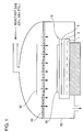
- Fig. 1 is a schematic cross section of a structure of a semiconductor manufacturing apparatus having a wafer holder according to one embodiment of the present invention.
- Fig. 2 is a schematic cross section of a structure of a wafer holder according to the one embodiment of the present invention.
- Fig. 3 is a perspective view illustrating that the outer shape of the structure under a heater is substantially the same as that of the structure over the heater.
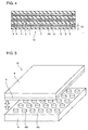
- Fig. 4 is a schematic cross section of a structure of a wafer holder having a gap.
- Fig. 5 is a perspective view of a structure of a wafer holder having supporters provided to a gap.
- Fig. 6 is a schematic cross section of the structure of the wafer holder having the supporters provided to the gap.
- Fig. 7 is a schematic cross section of a structure of a wafer holder having a conductive layer formed of two layers, i.e. a heater and another conductive layer.
- Fig. 8 is a schematic cross section of a structure of a wafer holder having a conductive layer formed of two layers, i.e. a heater and another conductive layer and further having a gap.
- Fig. 9 is a schematic cross section of a structure of a wafer holder having a conductive layer formed of a single heater layer.
- Fig. 10 is a schematic cross section of a structure of a wafer holder having a conductive layer formed of a single heater layer and further having a gap.
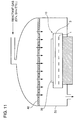
- Fig. 11 is a schematic cross section of a semiconductor manufacturing apparatus without a plasma generating electrode, to which a wafer holder in the embodiment of the present invention is applied.
- a semiconductor manufacturing apparatus is structured to mainly include in a vacuum container 50 a wafer holder 10, an upper electrode 30 for generating plasma, and a gas shower unit 40.
- Wafer holder 10 holds a wafer 20 on its surface and includes a heater 1 for heating wafer 20, a lower electrode 2 for generating plasma, and an electrostatic chuck electrode 3 for electrostatically securing wafer 20.
- wafer holder 10 in this embodiment has a structure in which heater 1, plasma generating lower electrode 2 and electrostatic chuck electrode 3 are each placed between ceramic base members 4 to be stacked on each other. Ceramic base members 4 are bonded to each other by a joint layer 5 made of an oxide such as glass, for example.
- a structure on the backside of heater 1, herein referred to as a backside structure A, has a heat insulating effect as shown in Fig. 2.
- One method of providing the heat insulating effect to the backside structure A is to provide, as a heat insulating structure, the backside structure A having a lower heat conductivity than that of a structure on the wafer holding surface side, herein referred to as a wafer holding side structure B.
- This structure can be obtained by using a material having a heat conductivity of at least 150 W/mK (e.g. aluminum nitride), for example, as ceramic base member 4 of the wafer holding side structure B and using ceramic having a lower heat conductivity of at most 100 W/mK as ceramic base member 4 of the backside structure A.
- the heat conductivity of 100 W/mK or less of ceramic base member 4 in the backside structure A is preferable since the heat insulating effect is enhanced.
- a material for ceramic base member 4 used in the backside structure A is at least one selected from the group consisting of aluminum nitride, aluminum oxide, silicon nitride and silicon carbide because of the corrosion resistance of these materials.
- the aluminum nitride is especially preferred.
- the side surface of the backside structure A has a small area, the side surface could be exposed to corrosive gas. Therefore, preferably the side surface is also formed of aluminum nitride having a heat conductivity of 100 W/mK or less.
- the aluminum nitride generally has a heat conductivity of approximately 170 W/mK.
- the simplest method for adjusting this heat conductivity of the aluminum nitride to 100 W/mK or less is to add for example oxygen, Si, transition metal and the like to the aluminum nitride and sinter the resultant aluminum nitride.
- this method is not the only method for obtaining a lower heat conductivity.
- joint layer 5 in the backside structure A has a heat conductivity of 10 W/mK or less since an enhanced heat insulating effect can be achieved.
- Joint layer 5 preferably has a thickness T1 of at least 10 ⁇ m. Further, it is possible to restrain heat from being transmitted by providing at least two joint layers 5 each having a thickness of at least 10 ⁇ m.
- the backside structure A may constitute a heat insulating structure (heat insulating layer) having an outer shape which is substantially the same as that of the wafer holding side structure B as shown in Fig. 3.
- heat insulating layer heat insulating layer
- respective peripheral surfaces of the backside structure A and the wafer holding side structure B form a continuing surface.
- the heat insulating structure can also be implemented by providing a gap 4A as shown in Fig. 4 between heater 1 and the backside of wafer holder 10, which remarkably increases the heat insulating effect of the backside structure A.
- the maximum heat insulating effect would be gained if gap 4A is a vacuum gap, however, a sufficient heat insulating effect could be gained even if gas is present in gap 4A.
- a required amount of heat to be generated in the wafer holder having gap 4A decreases by approximately 50% as compared with that in a wafer holder without such a gap if respective wafer heating surfaces are set at the same temperature.
- the wafer holder with gap 4A is accordingly highly effective in heat insulation for the backside. If gap 4A has a thickness of 0.01 mm or more, the heat insulating effect is remarkably high. At least two GAP layers 4A may be provided such that the total thickness of gap layers 4A along an arbitrary cross section is 0.01 mm or more.
- the backside structure A may be constituted of a porous material with a void (gap) having a total valid thickness of 0.01 mm along an arbitrary cross section.
- Gap 4A is produced by providing a depression in one or the other of ceramic base members and joining them. However, gap 4A could deteriorate the mechanical strength of holder 10. Accordingly, a plurality of supporters 4B are provided to gap 4A as shown in Figs. 5 and 6 to generate a composite structure for the purpose of enhancing the heat insulating effect while maintaining a necessary mechanical strength.
- Fig. 6 is a cross section of the structure shown in Fig. 5.
- the upper part is overlaid on the lower part.
- Plasma generating lower electrode 2 and electrostatic chuck electrode 3 are not shown in Figs. 3, 5 and 6 for convenience of description.
- the heat insulating structure as discussed above is applicable to a two-layer structure constituted of a heater layer 1 and a plasma generating lower electrode 2 or electrostatic chuck electrode 3 as shown in Figs. 7 and 8.
- a conductive layer above heater 1 may serve as both of the plasma generating lower electrode and electrostatic chuck electrode.
- the above heat insulating structure is applicable to a one-layer structure including a heater layer 1 only as shown in Figs. 9 and 10.
- the above heat insulating structure is applicable to a wafer holder 10 employed in a semiconductor manufacturing apparatus without using a plasma generating electrode as shown in Fig. 11. In this case, no plasma generating lower electrode is formed in wafer holder 10.
- the heat conductivity of ceramic base member 4 in the wafer holding side structure B is preferably at least 150 W/m for the purpose of speedily heating a wafer.
- a material for the ceramic base member 4 in the wafer holding side structure B is preferably at least one selected from the group consisting of aluminum nitride, aluminum oxide, silicon nitride and silicon carbide.
- the aluminum nitride is especially preferred.
- a superior heat insulating effect would be achieved by combining the structure in which ceramic base member 4 in the backside structure A has a lower heat conductivity than that of ceramic base member 4 in the wafer holding side structure B, the structure in which a heat insulating layer is formed in the backside structure A, and a structure in which a gap is provided between heater 1 and the backside of wafer holder 10, or combining arbitrary two of those structures so as to combine respective heat insulating effects.
- Sintered aluminum nitride piece can be produced by a conventional method.
- a sintering agent is first mixed with aluminum nitride powder. In consideration of corrosion resistance in actual use, a smaller amount of this agent is preferred.
- an organic binder is added for compacting as required. Any conventional method such as powder pressing and sheet forming is employed for compacting. Then, a heater circuit is formed. There are two methods for producing a heater circuit and post metalizing is one of the two.
- the compact piece is degreased and then sintered at a predetermined temperature. Any of known methods such as hot press, atmospheric sintering and HIP (hot isostatic pressing) may be employed for sintering.
- refractory metal such as W and Mo or a known wiring material such as Ag, Ag-Pd, Ag-Pt and Ni-Cr is formed into a required pattern. This pattern is generated, for example, by applying paste containing the above metal powder, agent for firing and binder are added so as to print a high precision pattern.
- the resultant piece is dried, degreased, and thereafter fired.
- Another method for producing a heater circuit is co-fire.
- paste containing refractory metal such as W and Mo mentioned above is applied onto the compact piece as mentioned above which has not been sintered, the compact piece is degreased, and thereafter the applied metal layer and aluminum nitride are simultaneously sintered.
- Metalized substrates produced by any of the above methods or a metalized substrate and a non-metalized substrate are joined to generate a structure in which heater 1 is embedded.
- respective metalized surfaces are never joined face to face.
- oxide layer joint layer 5 interposing therebetween such that heater circuit 1 is located between oxide layer 5 and the surface on which a wafer is held. If the substrates are joined such that oxide layer 5 is present between heater circuit 1 and the wafer holding surface, the efficiency deteriorates in heat transfer from the heater layer and a great amount of heat escapes to the backside when a semiconductor wafer on the holder is heated.
- Oxide layer 5 may be formed by being applied to a metalized or non-metalized surface and baked, or applied by thermal spraying. Alternatively, vapor deposition, CVD, PVD and the like may be employed for producing oxide layer 5, however, these methods are inferior in efficiency of forming a thick film. Oxide powder may be applied by printing or thermal spraying.
- Organic salt, inorganic salt, nitride, fluoride, or carbide may be used if the material is converted to oxide by heating thereof.
- Glass powder may be used as the oxide powder.
- the material for oxide layer 5 is not particularly limited to those mentioned above if oxide layer 5 formed of the material has a heat conductivity of 10 W/mK or less and can join substrates.
- Refractory metal paste obtained by kneading W powder and a sintering agent with an ethyl cellulose binder was applied onto one of the sheets of sintered pieces to form over the entire surface a pattern of a spiral heater line having a width of 1 mm and a line interval of 1 mm. Then, the metal paste was degreased in nitrogen at 800°C and baked in nitrogen at 1600°C to generate a heater line. On the other sheet of sintered piece having a dimension of ⁇ 300 mm X 1 mm, grass powder having a heat conductivity of 0.5 W/mK kneaded with an ethyl cellulose binder was printed to a thickness of 50 ⁇ m.
- the glass powder was degreased at 500°C on which the sintered piece having the heater line thereon was overlaid. They were fixed by a jig made of Mo, an weight of 500 g was placed thereon and accordingly joined in nitrogen at 800°C.
- the temperature of the surface of thus produced wafer holder was adjusted to become 700°C when current is applied with 200 V voltage.
- the amount of heat generated by the heater at this time was 2.0 W/mm 2 .
- a compact piece was prepared in the same manner as that in Example 1.
- Refractory metal paste containing W powder and a sintering agent kneaded with an ethyl cellulose binder was applied onto the compact piece.
- a print pattern to be produced by applying this paste was designed to have the same pattern as that in Example 1 after decreasing in size through sintering.
- the compact piece with the applied paste was degreased in nitrogen at 800°C and on which a compact piece having no such a paste applied thereon was overlaid.
- the stacked pieces were bonded by pressurizing them and thereafter sintered at 1800°C for 4 hours.
- the temperature of the surface of thus produced wafer holder was adjusted to become 700°C when current is applied with 200 V voltage.
- the amount of heat generated by the heater at this time was 2.6 W/mm 2 .
- a compact piece was prepared in the same manner as that in Example 1. On this compact piece, a heating element formed of a 0.5 mm Mo wire shaped into a spiral was placed thereon. Further, a molded piece of the same shape was placed thereon. They were then degreased in nitrogen at 800°C and placed in a mold formed of carbon to be hot-pressed at 1800°C for 4 hours. The resultant sintered piece had its top and bottom surfaces polished by diamond abrasive until the periphery decreases to ⁇ 300 mm. The sintered aluminum nitride piece had a heat conductivity of 170 W/mK and a thickness of 2 mm.
- the temperature of the surface of thus produced wafer holder was adjusted to become 700°C when current is applied with 200 V voltage.
- the amount of heat generated by the heater at this time was 2.8 W/mm 2 .
- a compact piece was prepared in the same manner as that in Example 1 to have a heat conductivity of 175 W/mK.
- refractory metal paste including W powder and a sintering agent kneaded with an ethyl cellulose binder was applied to form the same pattern as that of Example 1. This was degreased in nitrogen at 800°C and baked in nitrogen at 1600°C to produce a heater line.
- SiO 2 -based glass powder kneaded with an ethyl cellulose binder was printed.
- the temperature of the surface of thus produced wafer holder was adjusted to become 700°C when current is applied with 200 V voltage.
- the amount of heat generated by the heater at this time was 2.2 W/mm 2 .
- a sintered piece was prepared in the same manner as that in Example 1 such that the outer diameter would be ⁇ 320 mm after sintering and the heat conductivity was 175 W/mK.
- Refractory metal paste containing W powder and a sintering agent kneaded with an ethyl cellulose binder was applied on the sintered piece to form the same pattern as that of Example 1. This was degreased in nitrogen at 800°C and baked in nitrogen at 1600°C to produce a heater line. Further, a non-metalized substrate having a heat conductivity of 40 W/mK and a dimension of ⁇ 320 ⁇ 1 mm was prepared, and a depression of ⁇ 300 mm and 0.1 mm in depth was provided in the central area.
- SiO 2 -based glass powder kneaded with an ethyl cellulose binder was printed on the non-metalized substrate. This was degreased at 500°C and the sintered piece having the heater line formed thereon was overlaid on the non-metalized substrate. The sintered piece and the substrate were joined at the periphery of 10 mm in width. The joint was produced by fixing the sintered piece and the substrate by a jig formed of Mo, placing a weight of 500 g thereon, and heating them in nitrogen at 700°C.
- the temperature of the surface of thus produced wafer holder was adjusted to become 700°C when current is applied with 200 V voltage.
- the amount of heat generated by the heater at this time was 1.5 W/mm 2 .
- the present invention as heretofore described employs the structure in which ceramic on the backside relative to the heater has a lower heat conductivity than that of ceramic on the wafer holding side, the structure in which the heat insulating layer is formed on the backside relative to the heater, and the structure in which the gap is provided between the heater and the backside of the wafer holder.
- One of these structures or a combination of any structures can prevent heat from escaping to the backside of the heater thereby efficiently heating a wafer placed on the wafer holder. Accordingly, not only a rapid heating of a wafer but prevention of degradation in a seal provided under the holder are possible.
Landscapes
- Container, Conveyance, Adherence, Positioning, Of Wafer (AREA)
- Physical Vapour Deposition (AREA)
- Drying Of Semiconductors (AREA)
Abstract
Description
Claims (9)
- A wafer holder for a semiconductor manufacturing apparatus, said wafer holder including a heater (1) and a pair of ceramic base members (4) with said heater (1) interposing therebetween and having a wafer holding surface and a backside surface opposite each other with said heater (1) therebetween,
said ceramic base member (4) on the backside relative to said heater (1) being ceramic having a lower heat conductivity than ceramic on said wafer holding surface side relative to said heater (1). - A wafer holding for a semiconductor manufacturing apparatus, said wafer holder including heater (1) and a pair of ceramic base members (4) with said heater (1) interposing therebetween and having a wafer holding surface and a backside surface opposite each other with said heater (1) therebetween,
a heat insulating layer being formed on the backside relative to said heater (1). - A wafer holding for a semiconductor manufacturing apparatus, said wafer holder including a heater (1) and a pair of ceramic base members (4) with said heater (1) interposing therebetween and having a wafer holding surface and a backside surface opposite each other with said heater (1) therebetween,
a gap (4A) being provided between said heater (1) and said backside surface of said wafer holder (10). - A wafer holder for a semiconductor manufacturing apparatus, said wafer holder including a heater (1) and a pair of ceramic base members (4) with said heater (1) interposing therebetween and having a wafer holding surface and a backside surface opposite each other with said heater (1) therebetween,said ceramic base member (4) on the backside relative to said heater (1) being ceramic having a lower heat conductivity than ceramic on said wafer holding surface side relative to said heater (1),an insulating layer being formed on the backside relative to said heater (1), anda gap (4A) being provided between said heater (1) and said backside surface of said wafer holder (10).
- The wafer holder according to any one of claims 1 to 4, wherein said ceramic base (4) on the backside is formed of a material having a heat conductivity of at most 100 W/mK.
- The wafer holder according to any one of claims 1 to 5, wherein an intermediate layer (5) is formed between said ceramic base member (4) on the backside and said heater (1) and said intermediate layer (5) is a joint layer having a heat conductivity of at most 10 W/mK.
- The wafer holder according to claim 6, wherein said joint layer (5) has a thickness of at least 10 µm.
- The wafer holder according to any one of claims 1 to 7, wherein said ceramic base members (4) are formed of a material including at least one selected from aluminum nitride, aluminum oxide, silicon nitride and silicon carbide.
- The wafer holder for a semiconductor manufacturing apparatus according to any one of claims 3 to 8, wherein said gap (4A) has a thickness of at least 0.01 mm.
Applications Claiming Priority (2)
| Application Number | Priority Date | Filing Date | Title |
|---|---|---|---|
| JP2000012225 | 2000-01-20 | ||
| JP2000012225A JP2001203257A (en) | 2000-01-20 | 2000-01-20 | Wafer holder for semiconductor manufacturing equipment |
Publications (2)
| Publication Number | Publication Date |
|---|---|
| EP1119025A2 true EP1119025A2 (en) | 2001-07-25 |
| EP1119025A3 EP1119025A3 (en) | 2006-05-17 |
Family
ID=18539971
Family Applications (1)
| Application Number | Title | Priority Date | Filing Date |
|---|---|---|---|
| EP01300423A Withdrawn EP1119025A3 (en) | 2000-01-20 | 2001-01-18 | Wafer holder for semiconductor manufacturing apparatus |
Country Status (6)
| Country | Link |
|---|---|
| US (1) | US6365879B1 (en) |
| EP (1) | EP1119025A3 (en) |
| JP (1) | JP2001203257A (en) |
| KR (1) | KR100411215B1 (en) |
| CA (1) | CA2326093C (en) |
| TW (1) | TW475235B (en) |
Cited By (4)
| Publication number | Priority date | Publication date | Assignee | Title |
|---|---|---|---|---|
| EP1355347A3 (en) * | 2002-04-15 | 2003-12-10 | Sumitomo Electric Industries, Ltd. | Workpiece holder for semiconductor manufacturing apparatus |
| EP1363316A3 (en) * | 2002-04-24 | 2004-01-02 | Sumitomo Electric Industries, Ltd. | Ceramic susceptor |
| EP1528589A3 (en) * | 2003-10-31 | 2006-08-30 | Tokyo Electron Limited | Stage for placing target object |
| EP1764829A1 (en) * | 2000-01-20 | 2007-03-21 | Sumitomo Electric Industries, Ltd. | Wafer holder and semiconductor manufacturing apparatus comprising it |
Families Citing this family (27)
| Publication number | Priority date | Publication date | Assignee | Title |
|---|---|---|---|---|
| US20050211385A1 (en) | 2001-04-30 | 2005-09-29 | Lam Research Corporation, A Delaware Corporation | Method and apparatus for controlling spatial temperature distribution |
| EP1391140B1 (en) * | 2001-04-30 | 2012-10-10 | Lam Research Corporation | Method and apparatus for controlling the spatial temperature distribution across the surface of a workpiece support |
| US6847014B1 (en) * | 2001-04-30 | 2005-01-25 | Lam Research Corporation | Method and apparatus for controlling the spatial temperature distribution across the surface of a workpiece support |
| US6770852B1 (en) | 2003-02-27 | 2004-08-03 | Lam Research Corporation | Critical dimension variation compensation across a wafer by means of local wafer temperature control |
| KR100904361B1 (en) * | 2003-03-28 | 2009-06-23 | 도쿄엘렉트론가부시키가이샤 | Method and system for temperature control of a substrate |
| US8038796B2 (en) | 2004-12-30 | 2011-10-18 | Lam Research Corporation | Apparatus for spatial and temporal control of temperature on a substrate |
| TW200721363A (en) * | 2005-07-25 | 2007-06-01 | Sumitomo Electric Industries | Wafer holder, heater unit having the wafer holder, and wafer prober having the heater unit |
| US7525787B2 (en) * | 2005-09-30 | 2009-04-28 | Lam Research Corporation | Electrostatic chuck assembly with dielectric material and/or cavity having varying thickness, profile and/or shape, method of use and apparatus incorporating same |
| US20070181065A1 (en) * | 2006-02-09 | 2007-08-09 | General Electric Company | Etch resistant heater and assembly thereof |
| US9147588B2 (en) * | 2007-03-09 | 2015-09-29 | Tel Nexx, Inc. | Substrate processing pallet with cooling |
| CN102217054B (en) * | 2008-11-25 | 2013-05-08 | 京瓷株式会社 | Wafer heating apparatus, electrostatic chuck, and method for manufacturing wafer heating apparatus |
| WO2010090948A1 (en) * | 2009-02-04 | 2010-08-12 | Mattson Technology, Inc. | Electrostatic chuck system and process for radially tuning the temperature profile across the surface of a substrate |
| US8637794B2 (en) | 2009-10-21 | 2014-01-28 | Lam Research Corporation | Heating plate with planar heating zones for semiconductor processing |
| US8791392B2 (en) | 2010-10-22 | 2014-07-29 | Lam Research Corporation | Methods of fault detection for multiplexed heater array |
| KR20130107001A (en) * | 2012-03-21 | 2013-10-01 | 엘지이노텍 주식회사 | Apparatus for deposition |
| US10177014B2 (en) | 2012-12-14 | 2019-01-08 | Applied Materials, Inc. | Thermal radiation barrier for substrate processing chamber components |
| JP6290650B2 (en) * | 2014-02-24 | 2018-03-07 | 日本特殊陶業株式会社 | Heating device |
| JP6440298B2 (en) * | 2014-09-04 | 2018-12-19 | 国立大学法人 新潟大学 | Plasma etching equipment |
| JP6513938B2 (en) * | 2014-11-21 | 2019-05-15 | 日本特殊陶業株式会社 | Method of manufacturing electrostatic chuck |
| FR3039509B1 (en) * | 2015-07-28 | 2017-12-22 | Thales Sa | HEATING FOR AERONAUTICAL EQUIPMENT FOR AN AIRCRAFT |
| JP6583897B1 (en) * | 2018-05-25 | 2019-10-02 | ▲らん▼海精研股▲ふん▼有限公司 | Method for manufacturing ceramic electrostatic chuck |
| CN110911332B (en) * | 2018-09-14 | 2022-11-25 | 北京北方华创微电子装备有限公司 | Electrostatic chuck |
| US12313297B2 (en) * | 2020-01-27 | 2025-05-27 | Lexmark International, Inc. | Thin-walled tube heater for fluid |
| JP6971346B2 (en) * | 2020-03-06 | 2021-11-24 | ▲らん▼海精研股▲ふん▼有限公司 | Ceramic heaters with heat shielding effect and electrostatic chucks with ceramic heaters and their manufacturing methods |
| JP7550551B2 (en) * | 2020-06-30 | 2024-09-13 | 京セラ株式会社 | Electrostatic Chuck |
| WO2022108900A1 (en) * | 2020-11-19 | 2022-05-27 | Lam Research Corporation | Substrate support with uniform temperature across a substrate |
| US12185433B2 (en) * | 2022-05-17 | 2024-12-31 | Applied Materials, Inc. | High-temperature substrate support assembly with failure protection |
Family Cites Families (12)
| Publication number | Priority date | Publication date | Assignee | Title |
|---|---|---|---|---|
| US2007111A (en) * | 1931-10-17 | 1935-07-02 | Doherty Res Co | Glazed electric range heating unit and glaze therefor |
| US2799765A (en) * | 1955-01-31 | 1957-07-16 | Corning Glass Works | Electric heating unit |
| US5151871A (en) * | 1989-06-16 | 1992-09-29 | Tokyo Electron Limited | Method for heat-processing semiconductor device and apparatus for the same |
| JP2927857B2 (en) * | 1990-01-19 | 1999-07-28 | 株式会社東芝 | Substrate heating device |
| JP2604944B2 (en) | 1992-07-28 | 1997-04-30 | 日本碍子株式会社 | Semiconductor wafer heating equipment |
| TW444922U (en) * | 1994-09-29 | 2001-07-01 | Tokyo Electron Ltd | Heating device and the processing device using the same |
| JPH08227933A (en) * | 1995-02-20 | 1996-09-03 | Shin Etsu Chem Co Ltd | Wafer heating device with electrostatic adsorption function |
| US5671116A (en) * | 1995-03-10 | 1997-09-23 | Lam Research Corporation | Multilayered electrostatic chuck and method of manufacture thereof |
| JP2987085B2 (en) | 1995-06-28 | 1999-12-06 | 日本碍子株式会社 | Semiconductor wafer holding device, method of manufacturing the same, and method of using the same |
| JPH09213781A (en) * | 1996-02-01 | 1997-08-15 | Tokyo Electron Ltd | Mounting table structure and processing apparatus using the same |
| JPH11354260A (en) * | 1998-06-11 | 1999-12-24 | Shin Etsu Chem Co Ltd | Multi-layer ceramic heater |
| US6140624A (en) * | 1999-07-02 | 2000-10-31 | Advanced Ceramics Corporation | Pyrolytic boron nitride radiation heater |
-
2000
- 2000-01-20 JP JP2000012225A patent/JP2001203257A/en active Pending
- 2000-11-07 US US09/707,810 patent/US6365879B1/en not_active Expired - Lifetime
- 2000-11-16 CA CA002326093A patent/CA2326093C/en not_active Expired - Fee Related
-
2001
- 2001-01-16 TW TW090100925A patent/TW475235B/en not_active IP Right Cessation
- 2001-01-18 EP EP01300423A patent/EP1119025A3/en not_active Withdrawn
- 2001-01-19 KR KR10-2001-0003153A patent/KR100411215B1/en not_active Expired - Fee Related
Cited By (7)
| Publication number | Priority date | Publication date | Assignee | Title |
|---|---|---|---|---|
| EP1764829A1 (en) * | 2000-01-20 | 2007-03-21 | Sumitomo Electric Industries, Ltd. | Wafer holder and semiconductor manufacturing apparatus comprising it |
| EP1918990A1 (en) * | 2000-01-20 | 2008-05-07 | Sumitomo Electric Industries, Ltd. | Wafer holder for a semiconductor manufacturing apparatus |
| EP1355347A3 (en) * | 2002-04-15 | 2003-12-10 | Sumitomo Electric Industries, Ltd. | Workpiece holder for semiconductor manufacturing apparatus |
| EP1363316A3 (en) * | 2002-04-24 | 2004-01-02 | Sumitomo Electric Industries, Ltd. | Ceramic susceptor |
| US6806443B2 (en) | 2002-04-24 | 2004-10-19 | Sumitomo Electric Industries, Ltd. | Ceramic susceptor |
| EP1528589A3 (en) * | 2003-10-31 | 2006-08-30 | Tokyo Electron Limited | Stage for placing target object |
| US7183782B2 (en) | 2003-10-31 | 2007-02-27 | Tokyo Electron Limited | Stage for placing target object |
Also Published As
| Publication number | Publication date |
|---|---|
| CA2326093A1 (en) | 2001-07-20 |
| TW475235B (en) | 2002-02-01 |
| JP2001203257A (en) | 2001-07-27 |
| CA2326093C (en) | 2004-06-29 |
| KR20010076386A (en) | 2001-08-11 |
| KR100411215B1 (en) | 2003-12-18 |
| EP1119025A3 (en) | 2006-05-17 |
| US6365879B1 (en) | 2002-04-02 |
Similar Documents
| Publication | Publication Date | Title |
|---|---|---|
| CA2326093C (en) | Wafer holder for semiconductor manufacturing apparatus | |
| US6508884B2 (en) | Wafer holder for semiconductor manufacturing apparatus, method of manufacturing wafer holder, and semiconductor manufacturing apparatus | |
| US6460482B1 (en) | Gas shower unit for semiconductor manufacturing apparatus and semiconductor manufacturing apparatus | |
| JP3567855B2 (en) | Wafer holder for semiconductor manufacturing equipment | |
| JP2003017224A (en) | Resistance heating element circuit pattern and substrate processing apparatus using the same | |
| EP1363316B1 (en) | Ceramic susceptor | |
| US20050184054A1 (en) | Ceramics heater for semiconductor production system | |
| JP2004146566A (en) | Ceramic heater for semiconductor manufacturing equipment | |
| JP2002025913A (en) | Susceptor for semiconductor manufacturing device and semiconductor manufacturing device using the same | |
| JP2017147126A (en) | Manufacturing method of ceramic heater | |
| JP4529690B2 (en) | Wafer holder for semiconductor manufacturing apparatus, manufacturing method thereof, and semiconductor manufacturing apparatus | |
| US7394043B2 (en) | Ceramic susceptor | |
| JP2002173378A (en) | Method for manufacturing ceramic member for semiconductor processing equipment | |
| JP2005175508A (en) | Gas shower for semiconductor manufacturing equipment | |
| JP2002176096A (en) | Method for manufacturing ceramic member for semiconductor processing equipment | |
| JP4148180B2 (en) | Wafer holder for semiconductor manufacturing equipment | |
| JP2006286646A (en) | Ceramic heater |
Legal Events
| Date | Code | Title | Description |
|---|---|---|---|
| PUAI | Public reference made under article 153(3) epc to a published international application that has entered the european phase |
Free format text: ORIGINAL CODE: 0009012 |
|
| AK | Designated contracting states |
Kind code of ref document: A2 Designated state(s): AT BE CH CY DE DK ES FI FR GB GR IE IT LI LU MC NL PT SE TR |
|
| AX | Request for extension of the european patent |
Free format text: AL;LT;LV;MK;RO;SI |
|
| PUAL | Search report despatched |
Free format text: ORIGINAL CODE: 0009013 |
|
| AK | Designated contracting states |
Kind code of ref document: A3 Designated state(s): AT BE CH CY DE DK ES FI FR GB GR IE IT LI LU MC NL PT SE TR |
|
| AX | Request for extension of the european patent |
Extension state: AL LT LV MK RO SI |
|
| 17P | Request for examination filed |
Effective date: 20060725 |
|
| AKX | Designation fees paid |
Designated state(s): DE FR GB IT NL SE |
|
| 17Q | First examination report despatched |
Effective date: 20090223 |
|
| STAA | Information on the status of an ep patent application or granted ep patent |
Free format text: STATUS: THE APPLICATION IS DEEMED TO BE WITHDRAWN |
|
| 18D | Application deemed to be withdrawn |
Effective date: 20090707 |