EP1115198A2 - Frequency detector and phase-locked loop circuit including the detector - Google Patents
Frequency detector and phase-locked loop circuit including the detector Download PDFInfo
- Publication number
- EP1115198A2 EP1115198A2 EP00128707A EP00128707A EP1115198A2 EP 1115198 A2 EP1115198 A2 EP 1115198A2 EP 00128707 A EP00128707 A EP 00128707A EP 00128707 A EP00128707 A EP 00128707A EP 1115198 A2 EP1115198 A2 EP 1115198A2
- Authority
- EP
- European Patent Office
- Prior art keywords
- phase
- frequency
- detector
- signal
- input clock
- Prior art date
- Legal status (The legal status is an assumption and is not a legal conclusion. Google has not performed a legal analysis and makes no representation as to the accuracy of the status listed.)
- Granted
Links
Images


Classifications
-
- H—ELECTRICITY
- H03—ELECTRONIC CIRCUITRY
- H03D—DEMODULATION OR TRANSFERENCE OF MODULATION FROM ONE CARRIER TO ANOTHER
- H03D13/00—Circuits for comparing the phase or frequency of two mutually-independent oscillations
- H03D13/003—Circuits for comparing the phase or frequency of two mutually-independent oscillations in which both oscillations are converted by logic means into pulses which are applied to filtering or integrating means
- H03D13/004—Circuits for comparing the phase or frequency of two mutually-independent oscillations in which both oscillations are converted by logic means into pulses which are applied to filtering or integrating means the logic means delivering pulses at more than one terminal, e.g. up and down pulses
-
- H—ELECTRICITY
- H03—ELECTRONIC CIRCUITRY
- H03L—AUTOMATIC CONTROL, STARTING, SYNCHRONISATION OR STABILISATION OF GENERATORS OF ELECTRONIC OSCILLATIONS OR PULSES
- H03L7/00—Automatic control of frequency or phase; Synchronisation
- H03L7/06—Automatic control of frequency or phase; Synchronisation using a reference signal applied to a frequency- or phase-locked loop
- H03L7/08—Details of the phase-locked loop
- H03L7/085—Details of the phase-locked loop concerning mainly the frequency- or phase-detection arrangement including the filtering or amplification of its output signal
- H03L7/087—Details of the phase-locked loop concerning mainly the frequency- or phase-detection arrangement including the filtering or amplification of its output signal using at least two phase detectors or a frequency and phase detector in the loop
-
- H—ELECTRICITY
- H03—ELECTRONIC CIRCUITRY
- H03L—AUTOMATIC CONTROL, STARTING, SYNCHRONISATION OR STABILISATION OF GENERATORS OF ELECTRONIC OSCILLATIONS OR PULSES
- H03L7/00—Automatic control of frequency or phase; Synchronisation
- H03L7/06—Automatic control of frequency or phase; Synchronisation using a reference signal applied to a frequency- or phase-locked loop
- H03L7/08—Details of the phase-locked loop
- H03L7/085—Details of the phase-locked loop concerning mainly the frequency- or phase-detection arrangement including the filtering or amplification of its output signal
- H03L7/089—Details of the phase-locked loop concerning mainly the frequency- or phase-detection arrangement including the filtering or amplification of its output signal the phase or frequency detector generating up-down pulses
- H03L7/0891—Details of the phase-locked loop concerning mainly the frequency- or phase-detection arrangement including the filtering or amplification of its output signal the phase or frequency detector generating up-down pulses the up-down pulses controlling source and sink current generators, e.g. a charge pump
-
- H—ELECTRICITY
- H03—ELECTRONIC CIRCUITRY
- H03L—AUTOMATIC CONTROL, STARTING, SYNCHRONISATION OR STABILISATION OF GENERATORS OF ELECTRONIC OSCILLATIONS OR PULSES
- H03L7/00—Automatic control of frequency or phase; Synchronisation
- H03L7/06—Automatic control of frequency or phase; Synchronisation using a reference signal applied to a frequency- or phase-locked loop
- H03L7/16—Indirect frequency synthesis, i.e. generating a desired one of a number of predetermined frequencies using a frequency- or phase-locked loop
- H03L7/18—Indirect frequency synthesis, i.e. generating a desired one of a number of predetermined frequencies using a frequency- or phase-locked loop using a frequency divider or counter in the loop
Definitions
- the present invention relates to a frequency detector and a phase-locked loop (PLL) circuit that can detect a frequency difference using the detector built in the circuit.
- PLL phase-locked loop
- a PLL circuit is an important circuit applicable to various types of LSI systems of today.
- a known PLL circuit includes a PLL and a frequency controller.
- the PLL is made up of phase detector, charge pump, low-pass filter (LPF), voltage-controlled oscillator (VCO) and frequency divider.
- the frequency controller is provided to eliminate a frequency deviation from the PLL. In the PLL, if the gain of the VCO is decreased to enhance the noise immunity of the PLL, then the output frequency range of the VCO shrinks correspondingly, thus narrowing the frequency locking range of the PLL unintentionally.
- the PLL circuit is equipped with not only the phase detector that compares the phases of reference and oscillated clock signals to each other but also the frequency controller including a frequency detector that detects a frequency difference between these clock signals. That is to say, the PLL circuit utilizes two feedback loops so as not to narrow the frequency locking range. Specifically, in this case, the additional feedback loop, formed by the frequency detector, should have an increased gain, while the original phase-locked loop should have a decreased gain.
- the Wolaver's frequency detector includes a three-state phase detector and first and second additional detectors called “slip detectors". Responsive to a rising edge of a first or second input clock signal, the phase detector alternates among three states, thereby outputting first and second phase difference pulse signals. Each of the pulse signals represents a phase difference between the two input clock signals.
- the first slip detector includes two cascaded latches, receiving the first phase difference pulse signal at its clock input, and a device for delaying the first input clock signal.
- the second slip detector includes two cascaded latches, receiving the second phase difference pulse signal at its clock input, and a device for delaying the second input clock signal.
- the known frequency detector uses the phase difference pulse signals of the phase detector as clock signals for activating the initial-stage latches of the slip detectors. Accordingly, if the pulse width of the phase difference pulse signals is too narrow to set the initial-stage latches of the slip detectors, then the frequency difference will be detected erroneously.
- each of the delay devices for the slip detectors needs a large number of inverters. Accordingly, these inverters might generate noise and adversely affect the operation of the PLL circuit. Furthermore, the delay should be controlled so strictly that the operating range of the PLL circuit might be limited.
- Another object of the present invention is to provide a phase-locked loop circuit that can detect a frequency difference by using the frequency detector built in it.
- a frequency detector according to the present invention is realized just by connecting first and second latches to a three-state phase detector of the known type.
- the three-state phase detector includes first and second input terminals and first and second output terminals.
- the phase detector outputs first and second phase difference pulse signals through the first and second output terminals, respectively, by alternating among the following three states. If an effective edge of the first input clock signal is presented to the phase detector in a neutral state, then the phase detector is set to change into a first phase detection state. If an effective edge of the second input clock signal is presented to the phase detector in the neutral state, then the phase detector is set to change into a second phase detection state.
- the first latch latches the signal, which has been output through the first output terminal of the phase detector, responsive to an effective edge of the first input clock signal, and is reset responsive to the reset signal of the phase detector.
- the first latch outputs a first frequency difference pulse signal if two edges of the first input clock signal have been presented to the phase detector consecutively with no effective edges of the second input clock signal presented between the two edges.
- the second latch latches the signal, which has been output through the second output terminal of the phase detector, responsive to an effective edge of the second input clock signal, and is reset responsive to the reset signal of the phase detector.
- the second latch outputs a second frequency difference pulse signal if two edges of the second input clock signal have been presented to the phase detector consecutively with no effective edges of the first input clock signal presented between the two edges.
- a frequency detector is implementable just by connecting two latches to a three-state phase detector of the known type.
- the inventive frequency detector can be of a much smaller circuit size than the known ones.
- the phase difference pulse signals output from the three-state phase detector are not used as clock signals that activate the first-stage latches of slip detectors unlike the known frequency detector.
- the input clock signals for the phase detector are also used as clock signals for activating the two additional latches.
- the inventive frequency detector can have its operation stabilized even without controlling delays, for example. That is to say, the inventive frequency detector can advantageously be designed much more easily, and still can operate much more stably, than the known frequency detector.
- FIG. 1 is a block diagram illustrating an exemplary configuration for a PLL circuit according to the present invention.
- FIG. 2 is a block diagram illustrating a detailed configuration for the frequency detector shown in FIG. 1 .
- FIG. 3 is a diagram illustrating the state transition of the three-state phase detector shown in FIG. 2 .
- FIG. 4 is a block diagram illustrating an alternative configuration for the PLL circuit of the present invention.
- FIG. 5 is a block diagram illustrating a detailed configuration for the frequency detector shown in FIG. 4 .
- FIG. 1 illustrates an exemplary configuration for a PLL circuit according to the present invention.
- the PLL circuit includes three-state phase detector 10, first charge pump 11, LPF 12, VCO 13 and frequency divider 14, all of which together constitutes a PLL.
- the PLL circuit shown in FIG. 1 further includes a frequency controller 15 for eliminating a frequency deviation from the PLL. That is to say, the PLL circuit has frequency difference detection capabilities.
- the frequency controller 15 includes a frequency detector 20 and a second charge pump 21 .
- the frequency detector 20 receives a reference clock signal for the PLL and an oscillated clock signal, which has already had its frequency divided, as first and second input clock signals R and V , respectively.
- the second charge pump 21 receives the outputs of the frequency detector 20 through two terminals SU and SD and controls the oscillation frequency of the PLL responsive to these outputs.
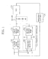
- FIG. 2 illustrates a detailed configuration for the frequency detector 20 shown in FIG. 1 .
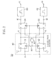
- the frequency detector 20 includes a three-state phase detector 40, two latches 50 and 51 and two isolated pulse generators 60 and 61 .
- the three-state phase detector 40 includes first and second input terminals and first and second output terminals. To detect a phase difference between the input R/V signals presented to the first and second input terminals, the phase detector 40 outputs first and second phase difference pulse signals VU and VD through the first and second output terminals, respectively, by alternating among the following three states. If a rising edge of the input R signal is presented to the phase detector 40 in a neutral state, then the detector 40 is set to change into a first phase detection state. If a rising edge of the input V signal is presented to the phase detector 40 in the neutral state, then the detector 40 is set to change into a second phase detection state.
- the phase detector 40 includes two latches 41 and 42 and one NAND gate 43.
- the latch 50 latches the VU signal responsive to a rising edge of the input R signal, and is reset responsive to the RST signal so as to output a first frequency difference pulse signal QU if two edges of the input R signal have been presented consecutively with no rising edges of the input V signal presented between those edges. That is to say, this latch 50 and the latch 41 in the phase detector 40 together constitute one shift register.
- the isolated pulse generator 60 is a circuit for making the pulse width of the QU signal constant and then outputting the QU signal with the constant width to the SU terminal.
- the pulse generator 60 may be a monostable multivibrator.
- the latch 51 latches the VD signal responsive to a rising edge of the input V signal, and is reset responsive to the RST signal so as to output a second frequency difference pulse signal QD if two edges of the input V signal have been presented consecutively with no rising edges of the input R signal presented between those edges. That is to say, this latch 51 and the latch 42 in the phase detector 40 together constitute one shift register.
- the isolated pulse generator 61 is a circuit for making the pulse width of the QD signal constant and then outputting the QD signal with the constant width to the SD terminal.
- the pulse generator 61 may also be a monostable multivibrator.
- FIG. 3 illustrates the state transitions of the three-state phase detector 40 shown in FIG. 2 .
- the first, second and third phases shown in FIG. 3 correspond to the neutral, first phase detection and second phase detection states, respectively. That is to say, the frequency detector 20 shown in FIG. 2 detects the state transitions indicated by the broken-line arrows in FIG. 3 . As can be seen from FIG. 3 , one of those transitions to be detected occurs where two rising edges of the input R signal have been presented consecutively, while the other occurs where two rising edges of the input V signal have been presented consecutively.
- the frequency detector 20 shown in FIG. 2 outputs a high-level (or H-level) signal in logic "1" state, representing that a frequency difference has been detected, as the QU or QD signal.
- the frequency detector 20 shown in FIG. 2 can have a circuit size much smaller than the known one.
- the input clock signals R/V for the three-state phase detector 40 are also used as activating clock signals for the additional latches 50 and 51, the frequency detector 20 can have its operation stabilized without controlling the delays, for example.
- the pulse widths of the QU and QD signals might change greatly depending on the frequencies of the input R/V signals or on a frequency difference between the R/V signals.
- the isolated pulse generators 60 and 61 are added to avoid such drastic change of the output pulse widths at the SU/SD terminals. In this manner, the responsiveness of the PLL circuit can be stabilized.
- the PLL circuit shown in FIG. 1 has two feedback loops, namely, the phase-locked loop that passes through the three-state phase detector 10 and the first charge pump 11 and a frequency control loop that passes through the frequency detector 20 and the second charge pump 21 . Accordingly, the gains of these two loops can be set independently. That is to say, even if the gain of the PLL is decreased, the locking range of the PLL circuit does not decrease correspondingly. Thus, the PLL circuit shown in FIG. 1 can not only have its noise immunity enhanced by reducing the loop gain of the PLL but also have its locking range broadened as well.
- FIG. 4 illustrates an alternative configuration for the PLL circuit of the present invention.
- the frequency controller 15 shown in FIG. 1 is replaced with a frequency controller 16 with a different configuration.
- the frequency controller 16 includes frequency detector 30, up/down counter 31, digital-to-analog converter (DAC) 32 and adder 33.
- the frequency detector 30 receives a reference clock signal for the PLL and an oscillated clock signal, which has already had its frequency divided, as the first and second input clock signals R and V, respectively.
- the up/down counter 31 receives the outputs of the frequency detector 30 through two terminals SU and SD and updates its count responsive to these outputs.
- the DAC 32 performs an analog control over the oscillation frequency of the PLL in accordance with the count of the up/down counter 31. Also, in the configuration shown in FIG. 4 , the oscillated clock signal, which has not had its frequency divided yet, is delivered to the frequency detector 30, up/down counter 31 and DAC 32. In FIG. 4, CK denotes a third clock signal input to the frequency detector 30 .
- FIG. 5 illustrates a detailed configuration for the frequency detector 30 shown in FIG. 4.
- the isolated pulse generators 60 and 61 shown in FIG. 2 are replaced with first and second counters 70 and 71, respectively.
- the first counter 70 starts counting the number of pulses of the input CK signal responsive to the output QU signal of the latch 50. And when its count reaches a predetermined number, the counter 70 is reset internally.
- the second counter 71 starts counting the number of pulses of the input CK signal responsive to the output QD signal of the latch 51. And when its count reaches a predetermined number, the counter 71 is also reset internally.
- the outputs of these two counters 70 and 71 are delivered to the up/down counter 31 via the SU/SD terminals, respectively.
- the frequency difference pulse signal QU or QD is input as a start pulse to the first or second counter 70 or 71.
- the first or second counter 70 or 71 starts counting the number of pulses of the input CK signal.
- the oscillated clock signal CK (which has not had its frequency divided yet) of the VCO 13 normally has a frequency much higher than that of the input clock signal R or V for the frequency detector 30. Accordingly, the oscillated clock signal CK can afford to be an activating clock signal for the first and second counters 70 and 71.
- any other clock signal may be used as the activating clock signal, it is most convenient to use the oscillated clock signal of the VCO 13 as the activating clock signal.
- the first or second counter 70 or 71 resets itself and stops counting. Accordingly, by setting the predetermined count to an arbitrary number, the frequency gain can be adjusted. In this manner, the frequency detector 30 shown in FIG. 5 can be easily connected to a digital circuit on a succeeding stage by digitally clocking (or outputting a count of) the output signal.
- the PLL circuit shown in FIG. 4 also has two feedback loops (i.e., the phase-locked loop and the frequency control loop), the loop gains of which can be set independently.
- the frequency control loop has the frequency detector 30, up/down counter 31 and DAC 32.
- the digital clock signal, output from the frequency detector 30, either increases or decreases the count of the up/down counter 31 , thereby changing the output of the DAC 32 and the oscillation frequency of the VCO 13 eventually. That is to say, the frequency control loop shown in FIG. 4 is controlled digitally. Accordingly, compared to a control loop consisting of analog circuits, the frequency control loop shown in FIG. 4 can enhance the noise immunity of the PLL circuit.
Landscapes
- Engineering & Computer Science (AREA)
- Power Engineering (AREA)
- Stabilization Of Oscillater, Synchronisation, Frequency Synthesizers (AREA)
- Manipulation Of Pulses (AREA)
Abstract
Description
Claims (5)
- A frequency detector comprising:a three-state phase detector including first and second input terminals and first and second output terminals, wherein to detect a phase difference between first and second input clock signals presented to the first and second input terminals, respectively, the phase detector outputs first and second phase difference pulse signals through the first and second output terminals, respectively, by alternating among three states in such a manner that:if an effective edge of the first input clock signal is presented to the phase detector in a neutral state, then the phase detector is set to change into a first phase detection state,if an effective edge of the second input clock signal is presented to the phase detector in the neutral state, then the phase detector is set to change into a second phase detection state andif effective edges of the first and second input clock signals are presented to the phase detector in this order or vice versa, then a reset signal is generated and the phase detector is reset and get back to the neutral state responsive to the reset signal;a first latch, which latches the signal, output through the first output terminal, responsive to an effective edge of the first input clock signal, and which is reset responsive to the reset, signal, the first latch outputting a first frequency difference pulse signal if two edges of the first input clock signal have been presented to the phase detector consecutively with no effective edges of the second input clock signal presented between the two edges; anda second latch, which latches the signal, output through the second output terminal, responsive to an effective edge of the second input clock signal, and which is reset responsive to the reset signal, the second latch outputting a second frequency difference pulse signal if two edges of the second input clock signal have been presented to the phase detector consecutively with no effective edges of the first input clock signal presented between the two edges.
- The frequency detector of Claim 1, further comprising circuit means for making pulse widths of the first and second frequency difference pulse signals constant and then outputting the first and second frequency difference pulse signals with the constant widths.
- The frequency detector of Claim 1, further comprising:a first counter, which starts counting the number of pulses of a third input clock signal responsive to the first frequency difference pulse signal and which is reset when the first counter counts a predetermined number; anda second counter, which starts counting the number of pulses of the third input clock signal responsive to the second frequency difference pulse signal and which is reset when the second counter counts another predetermined number.
- A phase-locked loop circuit comprising:a phase-locked loop; anda frequency controller for eliminating a frequency deviation from the phase-locked loop,wherein the frequency controller includes:a frequency detector according to Claim 2 for receiving reference and oscillated clock signals for the phase-locked loop as the first and second input clock signals, respectively; anda charge pump for controlling an oscillation frequency of the phase-locked loop responsive to the first and second frequency difference pulse signals that have been output from the frequency detector.
- A phase-locked loop circuit comprising:a phase-locked loop; anda frequency controller for eliminating a frequency deviation from the phase-locked loop,wherein the frequency controller includes:a frequency detector according to Claim 3 for receiving reference and oscillated clock signals for the phase-locked loop as the first and second input clock signals, respectively;an up/down counter for updating a count responsive to outputs of the first and second counters of the frequency detector; anda digital-to-analog converter for performing an analog control over an oscillation frequency of the phase-locked loop in accordance with the count of the up/down counter.
Applications Claiming Priority (2)
| Application Number | Priority Date | Filing Date | Title |
|---|---|---|---|
| JP2000005873 | 2000-01-07 | ||
| JP2000005873A JP3375584B2 (en) | 2000-01-07 | 2000-01-07 | Frequency comparator and phase-locked loop with it |
Publications (3)
| Publication Number | Publication Date |
|---|---|
| EP1115198A2 true EP1115198A2 (en) | 2001-07-11 |
| EP1115198A3 EP1115198A3 (en) | 2003-04-23 |
| EP1115198B1 EP1115198B1 (en) | 2004-03-03 |
Family
ID=18534490
Family Applications (1)
| Application Number | Title | Priority Date | Filing Date |
|---|---|---|---|
| EP00128707A Expired - Lifetime EP1115198B1 (en) | 2000-01-07 | 2000-12-29 | Frequency detector and phase-locked loop circuit including the detector |
Country Status (4)
| Country | Link |
|---|---|
| US (1) | US6407642B2 (en) |
| EP (1) | EP1115198B1 (en) |
| JP (1) | JP3375584B2 (en) |
| DE (1) | DE60008688T2 (en) |
Cited By (3)
| Publication number | Priority date | Publication date | Assignee | Title |
|---|---|---|---|---|
| EP3590191A1 (en) * | 2017-03-01 | 2020-01-08 | Telefonaktiebolaget LM Ericsson (Publ) | System for phase calibration of phase locked loop |
| CN111896078A (en) * | 2020-07-09 | 2020-11-06 | 合肥联睿微电子科技有限公司 | Bluetooth communication-based meter calibration method |
| US11595047B1 (en) * | 2022-03-03 | 2023-02-28 | Ciena Corporation | Apparatus and methods for a phase frequency detector with a wide operational range |
Families Citing this family (45)
| Publication number | Priority date | Publication date | Assignee | Title |
|---|---|---|---|---|
| US7039148B1 (en) * | 2001-04-27 | 2006-05-02 | Semtech Corporation | Phase detector and signal locking system controller |
| US6545545B1 (en) * | 2001-09-10 | 2003-04-08 | Micrel, Incorporated | Voltage-controlled oscillator frequency auto-calibrating system |
| US6566967B1 (en) * | 2002-02-26 | 2003-05-20 | Applied Micro Circuits Corporation | Configurable triple phase-locked loop circuit and method |
| US6642747B1 (en) * | 2002-03-15 | 2003-11-04 | National Semiconductor Corporation | Frequency detector for a phase locked loop system |
| EP1518325A1 (en) * | 2002-06-28 | 2005-03-30 | Advanced Micro Devices, Inc. | Phase-locked loop with automatic frequency tuning |
| US7551651B1 (en) * | 2003-01-27 | 2009-06-23 | Inphi Corporation | Method and system for time domain multiplexers with reduced inter-symbol interference |
| US7349514B2 (en) * | 2003-04-01 | 2008-03-25 | Seiko Epson Corporation | Frequency/phase locked loop clock synthesizer using an all digital frequency detector and an analog phase detector |
| DE10319899B4 (en) * | 2003-04-29 | 2006-07-06 | Infineon Technologies Ag | A method and frequency comparing means for generating a control signal indicative of a frequency deviation |
| US7480751B2 (en) * | 2003-09-08 | 2009-01-20 | Broadcom Corporation | Serial data interface system and method using a selectively accessed tone pattern generator |
| GB2426879C (en) * | 2003-12-12 | 2008-01-21 | Qualcomm Inc | A phase locked loop that sets gain automatically |
| KR100574980B1 (en) * | 2004-04-26 | 2006-05-02 | 삼성전자주식회사 | Phase-locked loop for fast frequency lock |
| US7038497B2 (en) * | 2004-04-28 | 2006-05-02 | Seiko Epson Corporation | Differential current mode phase/frequency detector circuit |
| US7154304B2 (en) * | 2004-07-13 | 2006-12-26 | Semtech Corporation | Enhanced phase and frequency detector that improves performance in the presence of a failing clock |
| KR100703366B1 (en) * | 2004-12-21 | 2007-04-03 | 삼성전자주식회사 | Noise Canceling Device for Wireless Transceiver |
| US20070170959A1 (en) * | 2006-01-24 | 2007-07-26 | Alessandro Minzoni | Phase detector |
| US7592847B2 (en) * | 2007-03-22 | 2009-09-22 | Mediatek Inc. | Phase frequency detector and phase-locked loop |
| JP4733152B2 (en) * | 2008-01-31 | 2011-07-27 | 日本電信電話株式会社 | Frequency control circuit and CDR circuit |
| US7683685B2 (en) * | 2008-02-05 | 2010-03-23 | Sony Corporation | System and method for implementing a digital phase-locked loop |
| EP2192689B1 (en) * | 2008-12-01 | 2012-01-18 | Samsung Electronics Co., Ltd. | Time-to-digital converter and all-digital phase-locked loop |
| US8164367B1 (en) * | 2009-01-15 | 2012-04-24 | Integrated Device Technology, Inc. | Spread spectrum clock generation technique for imaging applications |
| JP4682257B2 (en) * | 2009-03-30 | 2011-05-11 | 富士通株式会社 | Receiver |
| JP5365323B2 (en) * | 2009-04-20 | 2013-12-11 | ソニー株式会社 | Clock data recovery circuit and multiplied clock generation circuit |
| US8284816B1 (en) | 2009-06-01 | 2012-10-09 | Integrated Device Technology, Inc. | Push-pull spread spectrum clock signal generator |
| US8692621B2 (en) * | 2011-12-21 | 2014-04-08 | Fairchild Semiconductor Corporation | Methods and apparatus for oscillator frequency calibration |
| US9692429B1 (en) * | 2012-11-15 | 2017-06-27 | Gsi Technology, Inc. | Systems and methods involving fast-acquisition lock features associated with phase locked loop circuitry |
| US9444471B2 (en) * | 2013-06-06 | 2016-09-13 | Freescale Semiconductor, Inc. | Phase detector and phase-locked loop |
| DE112013007445B4 (en) * | 2013-11-08 | 2018-12-27 | Intel Corporation | Device for reducing the power of a charge pump |
| US9325490B2 (en) * | 2014-03-20 | 2016-04-26 | Stmicroelectronics International N.V. | Referenceless clock and data recovery circuit |
| US9520989B2 (en) * | 2014-07-28 | 2016-12-13 | Texas Instruments Incorporated | Phase detector and retimer for clock and data recovery circuits |
| US10891076B1 (en) | 2016-12-06 | 2021-01-12 | Gsi Technology, Inc. | Results processing circuits and methods associated with computational memory cells |
| US10770133B1 (en) | 2016-12-06 | 2020-09-08 | Gsi Technology, Inc. | Read and write data processing circuits and methods associated with computational memory cells that provides write inhibits and read bit line pre-charge inhibits |
| US10725777B2 (en) | 2016-12-06 | 2020-07-28 | Gsi Technology, Inc. | Computational memory cell and processing array device using memory cells |
| US10777262B1 (en) | 2016-12-06 | 2020-09-15 | Gsi Technology, Inc. | Read data processing circuits and methods associated memory cells |
| US10847213B1 (en) | 2016-12-06 | 2020-11-24 | Gsi Technology, Inc. | Write data processing circuits and methods associated with computational memory cells |
| US10943648B1 (en) | 2016-12-06 | 2021-03-09 | Gsi Technology, Inc. | Ultra low VDD memory cell with ratioless write port |
| US10998040B2 (en) | 2016-12-06 | 2021-05-04 | Gsi Technology, Inc. | Computational memory cell and processing array device using the memory cells for XOR and XNOR computations |
| US10847212B1 (en) | 2016-12-06 | 2020-11-24 | Gsi Technology, Inc. | Read and write data processing circuits and methods associated with computational memory cells using two read multiplexers |
| US11227653B1 (en) | 2016-12-06 | 2022-01-18 | Gsi Technology, Inc. | Storage array circuits and methods for computational memory cells |
| US10860320B1 (en) | 2016-12-06 | 2020-12-08 | Gsi Technology, Inc. | Orthogonal data transposition system and method during data transfers to/from a processing array |
| US10854284B1 (en) | 2016-12-06 | 2020-12-01 | Gsi Technology, Inc. | Computational memory cell and processing array device with ratioless write port |
| US10541691B1 (en) * | 2019-02-25 | 2020-01-21 | International Business Machines Corporation | Bang-bang phase detectors |
| US10930341B1 (en) | 2019-06-18 | 2021-02-23 | Gsi Technology, Inc. | Processing array device that performs one cycle full adder operation and bit line read/write logic features |
| US10958272B2 (en) | 2019-06-18 | 2021-03-23 | Gsi Technology, Inc. | Computational memory cell and processing array device using complementary exclusive or memory cells |
| US10877731B1 (en) | 2019-06-18 | 2020-12-29 | Gsi Technology, Inc. | Processing array device that performs one cycle full adder operation and bit line read/write logic features |
| KR102821931B1 (en) * | 2022-09-30 | 2025-06-17 | 주식회사 스카이칩스 | Phase Difference Control Circuit |
Family Cites Families (7)
| Publication number | Priority date | Publication date | Assignee | Title |
|---|---|---|---|---|
| US4902920A (en) * | 1988-09-26 | 1990-02-20 | General Signal Corporation | Extended range phase detector |
| US5079519A (en) * | 1991-02-14 | 1992-01-07 | Notorola, Inc. | Digital phase lock loop for a gate array |
| US5233314A (en) * | 1992-03-27 | 1993-08-03 | Cyrix Corporation | Integrated charge-pump phase-locked loop circuit |
| US5302916A (en) * | 1992-12-21 | 1994-04-12 | At&T Bell Laboratories | Wide range digital frequency detector |
| JP3094977B2 (en) * | 1997-11-28 | 2000-10-03 | 日本電気株式会社 | PLL circuit |
| US6256362B1 (en) * | 1998-06-30 | 2001-07-03 | Texas Instruments Incorporated | Frequency acquisition circuit and method for a phase locked loop |
| US6329847B1 (en) | 1998-09-29 | 2001-12-11 | U.S. Phillips Corporation | Radio device including a frequency synthesizer and phase discriminator for such a device |
-
2000
- 2000-01-07 JP JP2000005873A patent/JP3375584B2/en not_active Expired - Fee Related
- 2000-12-29 DE DE60008688T patent/DE60008688T2/en not_active Expired - Lifetime
- 2000-12-29 EP EP00128707A patent/EP1115198B1/en not_active Expired - Lifetime
-
2001
- 2001-01-03 US US09/752,525 patent/US6407642B2/en not_active Expired - Fee Related
Cited By (4)
| Publication number | Priority date | Publication date | Assignee | Title |
|---|---|---|---|---|
| EP3590191A1 (en) * | 2017-03-01 | 2020-01-08 | Telefonaktiebolaget LM Ericsson (Publ) | System for phase calibration of phase locked loop |
| CN111896078A (en) * | 2020-07-09 | 2020-11-06 | 合肥联睿微电子科技有限公司 | Bluetooth communication-based meter calibration method |
| CN111896078B (en) * | 2020-07-09 | 2022-05-13 | 合肥联睿微电子科技有限公司 | Bluetooth communication-based meter calibration method |
| US11595047B1 (en) * | 2022-03-03 | 2023-02-28 | Ciena Corporation | Apparatus and methods for a phase frequency detector with a wide operational range |
Also Published As
| Publication number | Publication date |
|---|---|
| JP2001196925A (en) | 2001-07-19 |
| JP3375584B2 (en) | 2003-02-10 |
| DE60008688D1 (en) | 2004-04-08 |
| DE60008688T2 (en) | 2004-07-29 |
| EP1115198A3 (en) | 2003-04-23 |
| US20010007436A1 (en) | 2001-07-12 |
| US6407642B2 (en) | 2002-06-18 |
| EP1115198B1 (en) | 2004-03-03 |
Similar Documents
| Publication | Publication Date | Title |
|---|---|---|
| US6407642B2 (en) | Frequency detector and phase-locked loop circuit including the detector | |
| EP0024878B1 (en) | Phase-locked loop circuit | |
| US5302916A (en) | Wide range digital frequency detector | |
| US4940952A (en) | Phase and frequency comparator circuit for phase locked loop | |
| KR100640568B1 (en) | Delay-locked loop circuit having master-slave structure | |
| US5406592A (en) | First order FLL/PLL system with low phase error | |
| US6133769A (en) | Phase locked loop with a lock detector | |
| JPH0677819A (en) | Phase restoration device of digital circuit | |
| US6054903A (en) | Dual-loop PLL with adaptive time constant reduction on first loop | |
| JP3984245B2 (en) | Phase lock loop and method for detecting lock situation in phase lock loop | |
| US6525612B2 (en) | Mode control of PLL circuit | |
| US5337022A (en) | Harmonic lock detector | |
| US6518845B2 (en) | PLL frequency synthesizer circuit | |
| US7496170B2 (en) | Digitally controlled oscillator having enhanced control resolution | |
| US6351154B2 (en) | Phase detector | |
| EP0367548B1 (en) | Sync detection circuit for phase-locked loop having frequency divider | |
| US5153725A (en) | Automatic frequency control circuit | |
| JP3080007B2 (en) | PLL circuit | |
| CN114244350A (en) | Charge-accelerated pump and phase-locked loop and method of operating the same | |
| EP0917292A2 (en) | Dual-loop phase-locked loop | |
| US7084670B1 (en) | Phase-frequency detector with gated reference clock input | |
| JP3079943B2 (en) | PLL circuit | |
| JP3407604B2 (en) | Latch miss detection circuit and PLL circuit | |
| JPH05304468A (en) | Phase locked loop circuit | |
| JPH0795051A (en) | Digital PLL circuit |
Legal Events
| Date | Code | Title | Description |
|---|---|---|---|
| PUAI | Public reference made under article 153(3) epc to a published international application that has entered the european phase |
Free format text: ORIGINAL CODE: 0009012 |
|
| AK | Designated contracting states |
Kind code of ref document: A2 Designated state(s): AT BE CH CY DE DK ES FI FR GB GR IE IT LI LU MC NL PT SE TR |
|
| AX | Request for extension of the european patent |
Free format text: AL;LT;LV;MK;RO;SI |
|
| PUAL | Search report despatched |
Free format text: ORIGINAL CODE: 0009013 |
|
| RIC1 | Information provided on ipc code assigned before grant |
Ipc: 7H 03L 7/087 B Ipc: 7H 03D 13/00 A Ipc: 7H 03L 7/089 B |
|
| AK | Designated contracting states |
Designated state(s): AT BE CH CY DE DK ES FI FR GB GR IE IT LI LU MC NL PT SE TR |
|
| AX | Request for extension of the european patent |
Extension state: AL LT LV MK RO SI |
|
| 17P | Request for examination filed |
Effective date: 20030523 |
|
| GRAP | Despatch of communication of intention to grant a patent |
Free format text: ORIGINAL CODE: EPIDOSNIGR1 |
|
| GRAS | Grant fee paid |
Free format text: ORIGINAL CODE: EPIDOSNIGR3 |
|
| AKX | Designation fees paid |
Designated state(s): DE FR GB |
|
| GRAA | (expected) grant |
Free format text: ORIGINAL CODE: 0009210 |
|
| AK | Designated contracting states |
Kind code of ref document: B1 Designated state(s): DE FR GB |
|
| REG | Reference to a national code |
Ref country code: GB Ref legal event code: FG4D |
|
| REG | Reference to a national code |
Ref country code: IE Ref legal event code: FG4D |
|
| REF | Corresponds to: |
Ref document number: 60008688 Country of ref document: DE Date of ref document: 20040408 Kind code of ref document: P |
|
| ET | Fr: translation filed | ||
| PLBE | No opposition filed within time limit |
Free format text: ORIGINAL CODE: 0009261 |
|
| STAA | Information on the status of an ep patent application or granted ep patent |
Free format text: STATUS: NO OPPOSITION FILED WITHIN TIME LIMIT |
|
| 26N | No opposition filed |
Effective date: 20041206 |
|
| PGFP | Annual fee paid to national office [announced via postgrant information from national office to epo] |
Ref country code: FR Payment date: 20101224 Year of fee payment: 11 |
|
| PGFP | Annual fee paid to national office [announced via postgrant information from national office to epo] |
Ref country code: GB Payment date: 20101229 Year of fee payment: 11 |
|
| PGFP | Annual fee paid to national office [announced via postgrant information from national office to epo] |
Ref country code: DE Payment date: 20101222 Year of fee payment: 11 |
|
| GBPC | Gb: european patent ceased through non-payment of renewal fee |
Effective date: 20111229 |
|
| REG | Reference to a national code |
Ref country code: FR Ref legal event code: ST Effective date: 20120831 |
|
| REG | Reference to a national code |
Ref country code: DE Ref legal event code: R119 Ref document number: 60008688 Country of ref document: DE Effective date: 20120703 |
|
| PG25 | Lapsed in a contracting state [announced via postgrant information from national office to epo] |
Ref country code: GB Free format text: LAPSE BECAUSE OF NON-PAYMENT OF DUE FEES Effective date: 20111229 Ref country code: DE Free format text: LAPSE BECAUSE OF NON-PAYMENT OF DUE FEES Effective date: 20120703 |
|
| PG25 | Lapsed in a contracting state [announced via postgrant information from national office to epo] |
Ref country code: FR Free format text: LAPSE BECAUSE OF NON-PAYMENT OF DUE FEES Effective date: 20120102 |