EP1113572A2 - Voltage-controlled oscillator and electronic device using same - Google Patents
Voltage-controlled oscillator and electronic device using same Download PDFInfo
- Publication number
- EP1113572A2 EP1113572A2 EP00128452A EP00128452A EP1113572A2 EP 1113572 A2 EP1113572 A2 EP 1113572A2 EP 00128452 A EP00128452 A EP 00128452A EP 00128452 A EP00128452 A EP 00128452A EP 1113572 A2 EP1113572 A2 EP 1113572A2
- Authority
- EP
- European Patent Office
- Prior art keywords
- voltage
- controlled oscillator
- terminal
- inductor
- frequency
- Prior art date
- Legal status (The legal status is an assumption and is not a legal conclusion. Google has not performed a legal analysis and makes no representation as to the accuracy of the status listed.)
- Granted
Links
Images


Classifications
-
- H—ELECTRICITY
- H03—ELECTRONIC CIRCUITRY
- H03B—GENERATION OF OSCILLATIONS, DIRECTLY OR BY FREQUENCY-CHANGING, BY CIRCUITS EMPLOYING ACTIVE ELEMENTS WHICH OPERATE IN A NON-SWITCHING MANNER; GENERATION OF NOISE BY SUCH CIRCUITS
- H03B5/00—Generation of oscillations using amplifier with regenerative feedback from output to input
- H03B5/08—Generation of oscillations using amplifier with regenerative feedback from output to input with frequency-determining element comprising lumped inductance and capacitance
- H03B5/12—Generation of oscillations using amplifier with regenerative feedback from output to input with frequency-determining element comprising lumped inductance and capacitance active element in amplifier being semiconductor device
- H03B5/1231—Generation of oscillations using amplifier with regenerative feedback from output to input with frequency-determining element comprising lumped inductance and capacitance active element in amplifier being semiconductor device the amplifier comprising one or more bipolar transistors
-
- H—ELECTRICITY
- H03—ELECTRONIC CIRCUITRY
- H03B—GENERATION OF OSCILLATIONS, DIRECTLY OR BY FREQUENCY-CHANGING, BY CIRCUITS EMPLOYING ACTIVE ELEMENTS WHICH OPERATE IN A NON-SWITCHING MANNER; GENERATION OF NOISE BY SUCH CIRCUITS
- H03B5/00—Generation of oscillations using amplifier with regenerative feedback from output to input
- H03B5/08—Generation of oscillations using amplifier with regenerative feedback from output to input with frequency-determining element comprising lumped inductance and capacitance
- H03B5/12—Generation of oscillations using amplifier with regenerative feedback from output to input with frequency-determining element comprising lumped inductance and capacitance active element in amplifier being semiconductor device
- H03B5/1203—Generation of oscillations using amplifier with regenerative feedback from output to input with frequency-determining element comprising lumped inductance and capacitance active element in amplifier being semiconductor device the amplifier being a single transistor
-
- H—ELECTRICITY
- H03—ELECTRONIC CIRCUITRY
- H03B—GENERATION OF OSCILLATIONS, DIRECTLY OR BY FREQUENCY-CHANGING, BY CIRCUITS EMPLOYING ACTIVE ELEMENTS WHICH OPERATE IN A NON-SWITCHING MANNER; GENERATION OF NOISE BY SUCH CIRCUITS
- H03B5/00—Generation of oscillations using amplifier with regenerative feedback from output to input
- H03B5/08—Generation of oscillations using amplifier with regenerative feedback from output to input with frequency-determining element comprising lumped inductance and capacitance
- H03B5/12—Generation of oscillations using amplifier with regenerative feedback from output to input with frequency-determining element comprising lumped inductance and capacitance active element in amplifier being semiconductor device
- H03B5/1237—Generation of oscillations using amplifier with regenerative feedback from output to input with frequency-determining element comprising lumped inductance and capacitance active element in amplifier being semiconductor device comprising means for varying the frequency of the generator
- H03B5/124—Generation of oscillations using amplifier with regenerative feedback from output to input with frequency-determining element comprising lumped inductance and capacitance active element in amplifier being semiconductor device comprising means for varying the frequency of the generator the means comprising a voltage dependent capacitance
- H03B5/1243—Generation of oscillations using amplifier with regenerative feedback from output to input with frequency-determining element comprising lumped inductance and capacitance active element in amplifier being semiconductor device comprising means for varying the frequency of the generator the means comprising a voltage dependent capacitance the means comprising voltage variable capacitance diodes
Definitions
- the present invention relates to a voltage-controlled oscillator and an electronic device employing the voltage-controlled oscillator, or more particularly, to a voltage-controlled oscillator adaptable to communication devices and an electronic device employing the voltage-controlled oscillator.
- a voltage-controlled oscillator whose frequency of oscillation can be varied diversely has been demanded along with prevalence of electronic devices including a portable telephone.
- a new printed-circuit board may be designed for each frequency of oscillation.
- this approach costs enormously.
- an inductive component to be included in a resonant circuit is realized with a strip line, the stripline is scraped in order to vary the inductance of the inductive component, and thus the frequency of oscillation of a voltage-controlled oscillator is varied.
- a labor for adjusting an electric characteristic such as a carrier-to-noise ratio includes scraping of the strip line included in the resonant circuit.
- Fig. 6 shows a conventional voltage-controlled oscillator.
- a voltage-controlled oscillator 3 consists mainly of a resonant circuit 31 and an amplification circuit 12.
- the resonant circuit 31 has one terminal of an inductor L1, which is a strip line, connected to the amplification circuit 12 via a capacitor C2.
- the other terminal of the inductor L1 is connected to the cathode of a variable-capacitance diode VD1.
- the cathode of the variable-capacitance diode VD1 is connected to a control voltage terminal a2 via an inductor L3 that is a choke coil.
- the anode of the variable-capacitance diode VD1 is grounded.
- the capacitor C2 is a coupling capacitor.
- the resonant circuit 31 is connected to the base of a transistor Tr1 serving as an amplification element in the amplification circuit 12.
- the emitter of the transistor Tr1 is connected to an output terminal a3 via a capacitor C7.
- the collector of the transistor Tr1 is grounded via a capacitor C4.
- a power terminal a4 is grounded via a capacitor C5, and connected to the collector of the transistor Tr1 via an inductor L4 that is a choke coil.
- the base and emitter of the transistor Tr1 are biased by resistors R1, R2, and R3.
- a capacitor C3 is connected between the base and emitter of the transistor Tr1.
- the inductance of the inductor L1 is adjusted in order to vary the frequency of oscillation of the voltage-controlled oscillator or improve the electric characteristic thereof such as a carrier-to-noise ratio.
- the inductor L1 is a circuit element enabling variation of the frequency of oscillation and greatly contributing to the electric characteristic such as the carrier-to-noise ratio.
- variable-capacitance diode VD1 and inductor L1 are connected in series with each other to thus realize a series resonant circuit suitable for expanding a frequency band within which the frequency of oscillation can be varied.
- the series resonant circuit has a property that when the frequency band within which the frequency of oscillation is variable is larger than 10 % of the frequency of oscillation, a loss caused by the resonant circuit 31 hardly depends on the frequency of oscillation.
- the inductor L1 included in the resonant circuit 31 having the series resonant circuit and realized with a strip line is scraped using a laser or the like in order to vary the frequency of oscillation of the voltage-controlled oscillator and to improve the electric characteristic thereof such as a carrier-to-noise ratio.
- an object of the present invention is to provide a voltage-controlled oscillator having a frequency of oscillation thereof readily varied and an electric characteristic thereof such as a carrier-to-noise ratio readily improved even when a frequency band within which the frequency of oscillation is variable is wide.
- Another object of the present invention is to provide a voltage-controlled oscillator whose frequency of oscillation can be varied greatly without the necessity of scraping a strip line.
- Still another object of the present invention is to provide a voltage-controlled oscillator having an electric characteristic thereof hardly degraded or a frequency of oscillation thereof hardly unsteadied even when a strip line is scraped in order to adjust part of a resonant circuit for the purpose of varying the frequency of oscillation or improving the electric characteristic such as a carrier-to-noise ratio.
- a voltage-controlled oscillator includes a resonant circuit and an amplification circuit.
- the resonant circuit includes an inductor whose one terminal is connected to the amplification circuit and whose the other terminal is grounded via a variable-capacitance diode, and a land to which a capacitor can be mounted.
- the first land has one terminal thereof connected to one terminal of the inductor and the other terminal thereof connected to the other terminal of the inductor.
- a voltage-controlled oscillator includes a resonant circuit and an amplification circuit.
- the resonant circuit includes an inductor whose one terminal is connected to the amplification circuit and whose the other terminal is grounded via a variable-capacitance diode, and a land to which a capacitor can be mounted.
- the land has one terminal thereof connected to one terminal of the inductor and the other terminal thereof grounded.
- a voltage-controlled oscillator includes a resonant circuit and an amplification circuit.
- the resonant circuit includes an inductor whose one terminal is connected to the amplification circuit and whose the other terminal is grounded via a variable-capacitance diode, and first and second lands to which a capacitor can be mounted.
- the first land has one terminal thereof connected to one terminal of the inductor and the other terminal thereof connected to the other terminal of the inductor.
- the second land has one terminal thereof connected to one terminal of the inductor and the other terminal thereof grounded.
- a voltage-controlled oscillator has a transmission line element interposed between the land and a ground terminal.
- a voltage-controlled oscillator has a transmission line element interposed between the variable-capacitance diode and a ground.
- the transmission line element in a voltage-controlled oscillator, has an adjustment terminal to change an impedance of the transmission line element by disconnecting from the ground terminal.
- an electronic device employs the foregoing voltage-controlled oscillator.
- a voltage-controlled oscillator in accordance with the present invention has its frequency of oscillation varied without the necessity of scraping an inductor through which a major signal passes. Therefore, the electric characteristic of the voltage-controlled oscillator will hardly be deteriorated and the frequency of oscillation thereof will hardly be unstable.
- a voltage-controlled oscillator in accordance with the present invention it is not necessary to scrape an inductor through which a major signal passes for the purpose of varying the frequency of oscillation thereof or improving a carrier-to-noise ratio thereof. Therefore, a chip coil exhibiting a high Q factor may be adopted as the inductor. In this case, the electric characteristic of the voltage-controlled oscillator such as the carrier-to-noise ratio can be improved.
- the frequency of oscillation of a voltage-controlled oscillator in accordance with the present invention can be varied greatly by changing the capacitances of discrete capacitors mounted to the first and second lands. It is not necessary to scrape a strip line. Otherwise it is possible to reduce an amount by which the strip line is scraped. Consequently, laboring efficiency improves.
- a magnitude by which the frequency of oscillation of a voltage-controlled oscillator in accordance with the present invention or the electric characteristic thereof such as a carrier-to-noise ratio can be adjusted varies depending on what portion of a transmission line element is cut. By selecting a proper portion of the transmission line, the frequency of oscillation or the electric characteristic such as a carrier-to-noise ratio can be adjusted properly.
- a resonant circuit of a voltage-controlled oscillator in accordance with the present invention includes first and second lands and a transmission line element as circuit elements used to adjust the frequency of oscillation of the voltage-controlled oscillator or the electric characteristic thereof such as a carrier-to-noise ratio.
- the first and second lands enable adjustment by a large magnitude.
- the line element enables adjustment by a small magnitude.
- a communication device in accordance with the present invention employs a voltage-controlled oscillator in accordance with the present invention having an electric characteristic thereof hardly degraded or a frequency of oscillation thereof hardly unsteadied.
- the communication device is therefore regarded as an electronic device enjoying an excellent output characteristics.
- Fig. 1 shows an embodiment of a voltage-controlled oscillator in accordance with the present invention.
- Fig. 1 the same reference numerals are assigned to components identical or equivalent to those shown in Fig. 6. The description of the components will be omitted.
- a resonant circuit 11 included in a voltage-controlled oscillator 1 has, in addition to the same components as the resonant circuit 31, a first land Land1, a second land Land2, a capacitor C1a, a capacitor C1b, and inductors L2a and L2b that are transmission line elements.
- the first land Land1 and second land Land2 are pairs of electrode patterns to which chip components are mounted.
- the capacitor C1a is mounted to the first land Land1, and the capacitor C1b is mounted to the second land Land2.
- One terminal of the inductor L1 is connected to one terminal of the first land Land1 and one terminal of the second land Land2, and also connected to an amplification circuit 12 via the capacitor C2.
- the other terminal of the inductor L1 is connected to the cathode of the variable-capacitance diode VD1 and to the other terminal of the first land Land1, and also connected to the control voltage terminal a2 via the inductor L3.
- the anode of the variable-capacitance diode VD1 is grounded via the inductor L2b.
- the other terminal of the second land Land2 is grounded via the inductor L2b.
- the inductors L2a and L2b are constituted of strip lines, and the capacitors C1a and C1b are constituted of known chip capacitors.
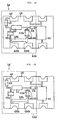
- Fig. 2A is a plan view of the voltage-controlled oscillator 1a whose frequency of oscillation is 1.8 GHz
- Fig. 2B is a plan view of the voltage-controlled oscillator 1a' whose frequency of oscillation is 3 GHz.
- the same reference numerals are assigned to identical or equivalent components. The description of the components will be not repeated.
- the voltage-controlled oscillators 1a and 1a' shown in Fig. 2A and Fig. 2B include resonant circuits 11a and 11a' respectively that do not include the first land Land1, capacitor C1a, and inductor L2a included in the resonant circuit 11 shown in Fig. 1. Circuit wirings, the second land Land2, and the inductors L1 and L2b that are strip lines are printed on a substrate 13 of each of the voltage-controlled oscillators 1a and 1a'.
- the capacitors C1b or C1b' and C2, variable-capacitance diode VD1, inductor L3, and amplification circuit 12 are mounted on the substrate 13.
- the first step is a step of removing the capacitor C1b from the second land Land2.
- the capacitor C1b is constituted of a chip capacitor, the capacitor C1b can be removed readily. If the frequency of oscillation of the voltage-controlled oscillator 1a becomes 3 GHz when the capacitor C1b is removed, the step described below need not be followed.
- the second step is a step of mounting the capacitor C1b', of which capacitance is different from that of the capacitor C1b, to the second land Land2.
- the capacitances of the capacitors C1b and Cb1' may be determined so that the frequency of oscillation of the voltage-controlled oscillator 1a is changed from 1.8 GHz to 3 GHz. This would greatly improve laboring efficiency.
- capacitance of the capacitor C1b as well as the inductor L1 greatly contributes to switching of the oscillation frequency.
- the capacitance of the capacitor C1b is changed to a proper capacitance with the property of the inductor L1 remaining original, the frequency of oscillation can be changed.
- the frequency of oscillation of a voltage-controlled oscillator can be varied diversely through the simple labor of mounting a chip capacitor having a proper capacitance to the second land Land2 on the same substrate on which a circuit pattern is printed.
- the method of changing the frequency of oscillation of the voltage-controlled oscillator 1a from one frequency to another has been described.
- the point of the present invention does not lie in varying the frequency of oscillation.
- the point of the present invention lies in that the frequency of oscillation of a voltage-controlled oscillator can be varied diversely depending on whether or not the capacitors C1a and C1b are mounted to the first land Land1 and second land Land2 or whatever capacitance a capacitor mounted has.
- the voltage-controlled oscillators 1a and 1a' each includes the inductor L2b that is a strip line. A major signal does not pass through the inductor L2b. Further, the inductor L2b relatively less affects the frequency of oscillation of the voltage-controlled oscillator or the electric characteristic thereof such as a carrier-to-noise ratio. After changing the oscillation frequency, if necessary, the oscillation frequency or the electric characteristic such. as a carrier-to-noise ratio can be adjusted finely by scraping the inductor L2b by a laser or the like in the voltage-controlled oscillator 1a and the voltage-controlled oscillator 1a'.
- Fig. 3 is an enlarged view of the inductor L2b.
- a method of finely adjusting the voltage-controlled oscillator 1a' will be described below. Assume that the frequency of oscillation of the voltage-controlled oscillator 1a' including the inductor L2b shown in Fig. 3 is 3 GHz. In this case, if the inductor L2b is cut along near a dot-dash line x1, the frequency of oscillation is lowered by approximately 80 MHz. If the inductor L2b is cut along near a dot-dash line x2, the frequency of oscillation is lowered by approximately 20 MHz.
- the frequency of oscillation is lowered by approximately 2 MHz.
- the frequency of oscillation can be varied by a desired value depending what portion of the inductor L2b is cut.
- the inductor L2b shown in Fig. 3 has an adjustment terminal g1 and an adjustment terminal g2 that are grounded. An impedance of the inductor L2b may be adjusted by disconnecting one of the adjustment terminals g1 and g2 from a ground.
- the inductor L2b shown in Fig. 3 may be cut along a dot-dash line x4 in order to adjust the frequency of oscillation.
- the frequency of oscillation or the electric characteristic such as a carrier-to-noise ratio can be varied within a large range.
- these portions of the inductor to be cut may be combined, whereby freedom in designing further expands. Consequently, a pattern space may not be widened but adjustment of the frequency of oscillation and improvement of the electric characteristic such as the carrier-to-noise ratio can be achieved easily.
- the frequency of oscillation of the voltage-controlled oscillator 1a is varied by replacing the capacitor C1b attached to the second land Land2 with the capacitor C1b'.
- Even the frequency of oscillation of the voltage-controlled oscillator 1 shown in Fig. 1 can be varied by replacing the capacitors C1a and C1b attached to the first land Land1 and second land Land2 with others in the same manner as that mentioned above or by breaking the inductors L2a and L2b in the same manner as that mentioned above.
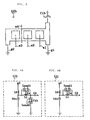
- Fig. 4A and Fig. 4B show a resonant circuit included in still another embodiment of the voltage-controlled oscillator in accordance with the present invention.
- Fig. 4A and Fig. 4B the same reference numerals are assigned to components identical to those shown in Fig. 1. The description of the components will be omitted.
- a resonant circuit 11b has the same circuit elements as the resonant circuit 11 shown in Fig. 1 but does not include the inductor L2a and inductor L2b.
- the resonant circuit 11b does not include the inductor L2a and inductor L2b that are strip lines.
- the capacitors C1a and C1b attached to the first land Land1 and second land Land2 are replaced with others, whereby the frequency of oscillation of the voltage-controlled oscillator can be altered. Even when one of the inductors L2a and L2b is removed, the same operations and advantages will be obtained.
- a resonant circuit 11c has a configuration excluding the second land Land2 and capacitor C1b shown in Fig. 4A.
- Fig. 4B may have the same circuit elements as removing the second land Land2 and capacitor C1b or only the capacitor C1b from the resonant circuit 11b shown in Fig. 4A.
- the capacitor C1a instead of the capacitor C1b is removed from the resonant circuit 11b shown in Fig. 4A, the same operations and advantages with the resonant circuit shown in Fig. 4B are obtained.
- the voltage-controlled oscillator in accordance with the present invention is not limited to the circuit elements employed in the embodiment to constitute a resonant circuit, amplification circuit, and a transmission line element.
- a microstrip line may be adopted as an inductor or a transmission line element.
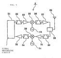
- Fig. 5 is a block diagram showing a communication device that is an embodiment of an electronic device in accordance with the present invention.
- a communication device 2 includes a signal processing circuit 21, bandpass filters 22, 26, 30, and 34, amplifiers 23, 27, 31, and 35, mixers 25 and 33, a duplexer 28, an antenna 29, and voltage-controlled oscillators 1b and 1c.
- an output terminal of the signal processing circuit 21 is connected to the mixer 25 via the bandpass filter 22 and amplifier 23 that are connected in series with each other.
- An output terminal of the voltage-controlled oscillator 1b is connected to the mixer 25.
- An output terminal of the mixer 25 is connected to the duplexer 28 connected to the antenna 29 via the bandpass filter 26 and amplifier 27 that are connected in series with each other.
- the duplexer 28 is connected to the mixer 33 via the bandpass filter 30 and amplifier 31 that are connected in series with each other.
- An output terminal of the voltage-controlled oscillator 1c is connected to the mixer 33.
- An output terminal of the mixer 33 is connected to the signal processing circuit 21 via the bandpass filter 34 and amplifier 35 that are connected in series with each other.
- an output signal of the signal processing circuit 21 has its unnecessary components removed by the bandpass filter 22.
- the resultant signal is amplified by the amplifier 23, and mixed with a signal output from the voltage-controlled oscillator 1b by the mixer 25.
- the signal is thus frequency-converted into a radio-frequency signal.
- the radio-frequency signal has its unnecessary components removed by the bandpass filter 26.
- the resultant signal is amplified by the amplifier 27, and radiated through the antenna 29 via the duplexer 28.
- a radio-frequency signal received through the antenna 29 is input to the bandpass filter 30 via the duplexer 28.
- the radio-frequency signal has its unnecessary components removed by the bandpass filter 30.
- the resultant signal is amplified by the amplifier 31, and mixed with a signal output from the voltage-controlled oscillator 1c by the mixer 33.
- the signal is thus frequency-converted into an intermediate-frequency signal.
- the intermediate-frequency signal has its unnecessary components removed by the bandpass filter 34.
- the resultant signal is amplified by the amplifier 35 and input to the signal processing circuit 21. Transmission and reception of a signal are thus carried out.
- the thus-configured communication device 2 is realized as an electronic device enjoying an excellent output capability owing to the inclusion of the voltage-controlled oscillators 1b and 1c each of which has the electric characteristic thereof hardly degraded or the frequency of oscillation thereof hardly unsteadied.
- the communication device 2 has been taken for instance in order to describe an electronic device employing a voltage-controlled oscillator in accordance with the present invention.
- the electronic device in accordance with the present invention is not limited to the communication device having the aforesaid configuration.
- the frequency of oscillation of a voltage-controlled oscillator can be varied without the necessity of scraping an inductor through which a major signal passes. Therefore, an electric characteristic of the voltage-controlled oscillator will not be degraded and the frequency of oscillation thereof will not be unsteadied.
- an inductor through which a major signal passes, for the purpose of varying the frequency of oscillation of a voltage-controlled oscillator or improving a carrier-to-noise ratio thereof.
- a chip coil exhibiting a high Q factor can be adopted as the inductor. In this case, the electric characteristic such as the carrier-to-noise ratio can be improved.
- the frequency of oscillation of a voltage-controlled oscillator can be varied greatly by changing the capacitances of capacitors attached to first and second lands. This obviates the necessity of scraping a strip line. Otherwise, the magnitude of scraping can be reduced. Consequently, laboring efficiency improves.
- a magnitude of adjustment of the frequency of oscillation of a voltage-controlled oscillator or an electric characteristic such as a carrier-to-noise ratio thereof varies depending on what portion of a line element is cut. Consequently, the frequency of oscillation and the electric characteristic such as the carrier-to-noise ratio can be adjusted readily by selecting a proper portion of the line element.
- a resonant circuit included in a voltage-controlled oscillator includes first and second lands and a line element as circuit elements used to adjust the frequency of oscillation of the voltage-controlled oscillator or an electric characteristic thereof such as a carrier-to-noise ratio.
- the first and second land enable adjustment by a large magnitude, while the line element enables adjustment by a minute magnitude. Consequently, freedom in designing expands, and the frequency of oscillation or the electric characteristic such as the carrier-to-noise ratio can be adjusted readily.
- a communication device employs a voltage-controlled oscillator in accordance with the present invention that has an electric characteristic thereof hardly degraded and a frequency of oscillation thereof hardly unsteadied.
- the communication device is therefore provided as an electric device enjoying an excellent output capability.
Landscapes
- Inductance-Capacitance Distribution Constants And Capacitance-Resistance Oscillators (AREA)
Abstract
Description
Claims (9)
- A voltage-controlled oscillator comprising a resonant circuit and an amplification circuit,wherein said resonant circuit comprises an inductor having one terminal thereof connected to said amplification circuit and the other terminal thereof grounded via a variable-capacitance diode, and a land to which a capacitor is mounted; andsaid land has one terminal thereof connected to one terminal of said inductor and the other terminal thereof connected to the other terminal of said inductor.
- A voltage-controlled oscillator comprising a resonant circuit and an amplification circuit,wherein said resonant circuit comprises an inductor having one terminal thereof connected to said amplification circuit and the other terminal thereof grounded via a variable-capacitance diode, and a land to which a capacitor can be mounted; andsaid land has one terminal thereof connected to one terminal of said inductor and the other terminal thereof grounded.
- A voltage-controlled oscillator comprising a resonant circuit and an amplification circuit,wherein said resonant circuit comprises an inductor having one terminal thereof connected to said amplification circuit and the other terminal thereof grounded via a variable-capacitance diode, and first and second lands to which a capacitor can be mounted; andsaid first land has one terminal thereof connected to one terminal of said inductor and the other terminal thereof connected to the other terminal of said inductor, and said second land has one terminal thereof connected to one terminal of said inductor and the other terminal thereof grounded.
- A voltage-controlled oscillator according to Claim 2, wherein a transmission line element is interposed between said land and a ground.
- A voltage-controlled oscillator according to Claim 3, wherein a transmission line element is interposed between said second land and a ground.
- A voltage-controlled oscillator according to any of Claims 1 to 5, wherein a transmission line element is interposed between said variable-capacitance diode and a ground.
- A voltage-controlled oscillator according to Claim 4 or 5, wherein said transmission line element has an adjustment terminal to change an impedance thereof by disconnecting from the ground.
- A voltage-controlled oscillator according to Claim 6, wherein said transmission line element has an adjustment terminal to change an impedance thereof by disconnecting from the ground.
- An electronic device employing a voltage-controlled oscillator set forth in any of Claims 1 to 3.
Applications Claiming Priority (4)
| Application Number | Priority Date | Filing Date | Title |
|---|---|---|---|
| JP36475699 | 1999-12-22 | ||
| JP36475699 | 1999-12-22 | ||
| JP2000370250A JP3740977B2 (en) | 1999-12-22 | 2000-12-05 | Voltage-controlled oscillator and electronic device using the same |
| JP2000370250 | 2000-12-05 |
Publications (3)
| Publication Number | Publication Date |
|---|---|
| EP1113572A2 true EP1113572A2 (en) | 2001-07-04 |
| EP1113572A3 EP1113572A3 (en) | 2002-05-02 |
| EP1113572B1 EP1113572B1 (en) | 2004-01-14 |
Family
ID=26581609
Family Applications (1)
| Application Number | Title | Priority Date | Filing Date |
|---|---|---|---|
| EP00128452A Expired - Lifetime EP1113572B1 (en) | 1999-12-22 | 2000-12-22 | Voltage-controlled oscillator and electronic device using same |
Country Status (4)
| Country | Link |
|---|---|
| US (1) | US6456169B2 (en) |
| EP (1) | EP1113572B1 (en) |
| JP (1) | JP3740977B2 (en) |
| DE (1) | DE60007714T2 (en) |
Families Citing this family (5)
| Publication number | Priority date | Publication date | Assignee | Title |
|---|---|---|---|---|
| US6864755B2 (en) | 2000-10-06 | 2005-03-08 | Alfred E. Mann Institute For Biomedical Engineering At The University Of Southern California | Switched reactance modulated E-class oscillator design |
| US7005935B2 (en) * | 2001-10-05 | 2006-02-28 | Alfred E. Mann Institute For Biomedical Engineering At The University Of Southern California | Switched reactance modulated E-class oscillator |
| JP4815741B2 (en) * | 2003-12-11 | 2011-11-16 | 株式会社村田製作所 | High frequency module |
| JP2006261823A (en) * | 2005-03-15 | 2006-09-28 | Alps Electric Co Ltd | Oscillation circuit |
| US9917547B2 (en) * | 2013-01-09 | 2018-03-13 | Nxp Usa, Inc. | Voltage controlled oscillator |
Family Cites Families (10)
| Publication number | Priority date | Publication date | Assignee | Title |
|---|---|---|---|---|
| US3614665A (en) * | 1970-04-06 | 1971-10-19 | Avco Corp | Voltage-controlled oscillator with digital preset |
| JPS56149405A (en) | 1980-04-23 | 1981-11-19 | Showa Denko Kk | Production of ethylene polymer |
| US4360867A (en) * | 1980-12-08 | 1982-11-23 | Bell Telephone Laboratories, Incorporated | Broadband frequency multiplication by multitransition operation of step recovery diode |
| DE3246295C2 (en) | 1982-12-14 | 1986-11-27 | Siemens AG, 1000 Berlin und 8000 München | Frequency modulable oscillator |
| JPS59149405A (en) * | 1983-02-16 | 1984-08-27 | Matsushita Electric Ind Co Ltd | local oscillator |
| JPS6062705A (en) | 1984-07-26 | 1985-04-10 | Matsushita Electric Ind Co Ltd | Voltage controlled variable frequency oscillator |
| JPH06196928A (en) | 1992-12-25 | 1994-07-15 | Murata Mfg Co Ltd | Voltage control type oscillation circuit |
| FI97925C (en) * | 1994-06-21 | 1997-03-10 | Nokia Mobile Phones Ltd | A voltage controlled oscillator circuit with improved tuning linearity |
| JPH1051234A (en) * | 1996-08-05 | 1998-02-20 | Tdk Corp | Voltage control oscillator and its control method |
| JP3829525B2 (en) | 1998-04-02 | 2006-10-04 | セイコーエプソン株式会社 | Capacitance array unit and oscillation circuit |
-
2000
- 2000-12-05 JP JP2000370250A patent/JP3740977B2/en not_active Expired - Fee Related
- 2000-12-22 US US09/746,896 patent/US6456169B2/en not_active Expired - Fee Related
- 2000-12-22 DE DE60007714T patent/DE60007714T2/en not_active Expired - Lifetime
- 2000-12-22 EP EP00128452A patent/EP1113572B1/en not_active Expired - Lifetime
Also Published As
| Publication number | Publication date |
|---|---|
| US6456169B2 (en) | 2002-09-24 |
| EP1113572A3 (en) | 2002-05-02 |
| JP2001244738A (en) | 2001-09-07 |
| US20010006358A1 (en) | 2001-07-05 |
| JP3740977B2 (en) | 2006-02-01 |
| EP1113572B1 (en) | 2004-01-14 |
| DE60007714T2 (en) | 2004-12-02 |
| DE60007714D1 (en) | 2004-02-19 |
Similar Documents
| Publication | Publication Date | Title |
|---|---|---|
| KR100558276B1 (en) | Double resonant antenna device | |
| EP0803972B1 (en) | Dual band oscillator circuit | |
| US20100060362A1 (en) | Cascode circuit | |
| US7206551B2 (en) | High frequency switch module and multi-layer substrate for high frequency switch module | |
| US12451855B2 (en) | Filter device and radio-frequency front-end circuit including the same | |
| US7292113B2 (en) | Multi-octave band tunable coupled-resonator oscillator | |
| US6411168B2 (en) | Voltage-controlled oscillator and communication apparatus using same | |
| EP1113572B1 (en) | Voltage-controlled oscillator and electronic device using same | |
| EP1931028B1 (en) | Variable tuning circuit using variable capacitance diode and television tuner | |
| US7605670B2 (en) | User-definable low cost, low noise, and phase hit insensitive multi-octave-band tunable oscillator | |
| US6724274B2 (en) | Frequency-switching oscillator and electronic device using the same | |
| CN1371167A (en) | Voltage controlled variable tuning circuit for changing vibrating frequency band of voltage controlled vibrator | |
| US7696833B2 (en) | Oscillator | |
| JPH104315A (en) | High frequency oscillation circuit | |
| KR20020084776A (en) | Voltage controlled oscillator for multi-band | |
| JP2005136836A (en) | Multiplication oscillator circuit and radio communication apparatus using the same | |
| JP3764688B2 (en) | Voltage controlled oscillator | |
| JP2003101344A (en) | Frequency shift type high frequency voltage control type oscillation circuit | |
| CA2533623C (en) | Tunable oscillator | |
| KR20050049413A (en) | Oscillator | |
| JP2003179431A (en) | Frequency shift type high frequency voltage control type oscillation circuit | |
| JP2003101345A (en) | Frequency shift type voltage controlled oscillator | |
| KR19990058814A (en) | Voltage Controlled Oscillator Using Coaxial Resonator | |
| JP2005304085A (en) | Voltage controlled oscillator | |
| JP2003078350A (en) | High frequency voltage controlled oscillator |
Legal Events
| Date | Code | Title | Description |
|---|---|---|---|
| PUAI | Public reference made under article 153(3) epc to a published international application that has entered the european phase |
Free format text: ORIGINAL CODE: 0009012 |
|
| 17P | Request for examination filed |
Effective date: 20001222 |
|
| AK | Designated contracting states |
Kind code of ref document: A2 Designated state(s): AT BE CH CY DE DK ES FI FR GB GR IE IT LI LU MC NL PT SE TR Kind code of ref document: A2 Designated state(s): DE FI FR SE |
|
| AX | Request for extension of the european patent |
Free format text: AL;LT;LV;MK;RO;SI |
|
| PUAL | Search report despatched |
Free format text: ORIGINAL CODE: 0009013 |
|
| AK | Designated contracting states |
Kind code of ref document: A3 Designated state(s): AT BE CH CY DE DK ES FI FR GB GR IE IT LI LU MC NL PT SE TR |
|
| AX | Request for extension of the european patent |
Free format text: AL;LT;LV;MK;RO;SI |
|
| 17Q | First examination report despatched |
Effective date: 20020913 |
|
| AKX | Designation fees paid |
Free format text: DE FI FR SE |
|
| GRAH | Despatch of communication of intention to grant a patent |
Free format text: ORIGINAL CODE: EPIDOS IGRA |
|
| GRAS | Grant fee paid |
Free format text: ORIGINAL CODE: EPIDOSNIGR3 |
|
| GRAA | (expected) grant |
Free format text: ORIGINAL CODE: 0009210 |
|
| AK | Designated contracting states |
Kind code of ref document: B1 Designated state(s): DE FI FR SE |
|
| PG25 | Lapsed in a contracting state [announced via postgrant information from national office to epo] |
Ref country code: FI Free format text: LAPSE BECAUSE OF FAILURE TO SUBMIT A TRANSLATION OF THE DESCRIPTION OR TO PAY THE FEE WITHIN THE PRESCRIBED TIME-LIMIT Effective date: 20040114 |
|
| REG | Reference to a national code |
Ref country code: IE Ref legal event code: FG4D |
|
| REF | Corresponds to: |
Ref document number: 60007714 Country of ref document: DE Date of ref document: 20040219 Kind code of ref document: P |
|
| PG25 | Lapsed in a contracting state [announced via postgrant information from national office to epo] |
Ref country code: SE Free format text: LAPSE BECAUSE OF FAILURE TO SUBMIT A TRANSLATION OF THE DESCRIPTION OR TO PAY THE FEE WITHIN THE PRESCRIBED TIME-LIMIT Effective date: 20040414 |
|
| ET | Fr: translation filed | ||
| PLBE | No opposition filed within time limit |
Free format text: ORIGINAL CODE: 0009261 |
|
| STAA | Information on the status of an ep patent application or granted ep patent |
Free format text: STATUS: NO OPPOSITION FILED WITHIN TIME LIMIT |
|
| 26N | No opposition filed |
Effective date: 20041015 |
|
| PGFP | Annual fee paid to national office [announced via postgrant information from national office to epo] |
Ref country code: FR Payment date: 20101224 Year of fee payment: 11 |
|
| PGFP | Annual fee paid to national office [announced via postgrant information from national office to epo] |
Ref country code: DE Payment date: 20101215 Year of fee payment: 11 |
|
| REG | Reference to a national code |
Ref country code: FR Ref legal event code: ST Effective date: 20120831 |
|
| REG | Reference to a national code |
Ref country code: DE Ref legal event code: R119 Ref document number: 60007714 Country of ref document: DE Effective date: 20120703 |
|
| PG25 | Lapsed in a contracting state [announced via postgrant information from national office to epo] |
Ref country code: DE Free format text: LAPSE BECAUSE OF NON-PAYMENT OF DUE FEES Effective date: 20120703 |
|
| PG25 | Lapsed in a contracting state [announced via postgrant information from national office to epo] |
Ref country code: FR Free format text: LAPSE BECAUSE OF NON-PAYMENT OF DUE FEES Effective date: 20120102 |