EP1111974A2 - Process for manufacturing a solder connection - Google Patents
Process for manufacturing a solder connection Download PDFInfo
- Publication number
- EP1111974A2 EP1111974A2 EP00127521A EP00127521A EP1111974A2 EP 1111974 A2 EP1111974 A2 EP 1111974A2 EP 00127521 A EP00127521 A EP 00127521A EP 00127521 A EP00127521 A EP 00127521A EP 1111974 A2 EP1111974 A2 EP 1111974A2
- Authority
- EP
- European Patent Office
- Prior art keywords
- contact point
- solder
- connection element
- connection
- annular gap
- Prior art date
- Legal status (The legal status is an assumption and is not a legal conclusion. Google has not performed a legal analysis and makes no representation as to the accuracy of the status listed.)
- Granted
Links
Images

Classifications
-
- H—ELECTRICITY
- H05—ELECTRIC TECHNIQUES NOT OTHERWISE PROVIDED FOR
- H05K—PRINTED CIRCUITS; CASINGS OR CONSTRUCTIONAL DETAILS OF ELECTRIC APPARATUS; MANUFACTURE OF ASSEMBLAGES OF ELECTRICAL COMPONENTS
- H05K3/00—Apparatus or processes for manufacturing printed circuits
- H05K3/30—Assembling printed circuits with electric components, e.g. with resistor
- H05K3/32—Assembling printed circuits with electric components, e.g. with resistor electrically connecting electric components or wires to printed circuits
- H05K3/34—Assembling printed circuits with electric components, e.g. with resistor electrically connecting electric components or wires to printed circuits by soldering
- H05K3/3447—Lead-in-hole components
-
- H—ELECTRICITY
- H05—ELECTRIC TECHNIQUES NOT OTHERWISE PROVIDED FOR
- H05K—PRINTED CIRCUITS; CASINGS OR CONSTRUCTIONAL DETAILS OF ELECTRIC APPARATUS; MANUFACTURE OF ASSEMBLAGES OF ELECTRICAL COMPONENTS
- H05K2201/00—Indexing scheme relating to printed circuits covered by H05K1/00
- H05K2201/09—Shape and layout
- H05K2201/09209—Shape and layout details of conductors
- H05K2201/09654—Shape and layout details of conductors covering at least two types of conductors provided for in H05K2201/09218 - H05K2201/095
- H05K2201/0979—Redundant conductors or connections, i.e. more than one current path between two points
-
- H—ELECTRICITY
- H05—ELECTRIC TECHNIQUES NOT OTHERWISE PROVIDED FOR
- H05K—PRINTED CIRCUITS; CASINGS OR CONSTRUCTIONAL DETAILS OF ELECTRIC APPARATUS; MANUFACTURE OF ASSEMBLAGES OF ELECTRICAL COMPONENTS
- H05K2201/00—Indexing scheme relating to printed circuits covered by H05K1/00
- H05K2201/10—Details of components or other objects attached to or integrated in a printed circuit board
- H05K2201/10227—Other objects, e.g. metallic pieces
- H05K2201/10295—Metallic connector elements partly mounted in a hole of the PCB
- H05K2201/10303—Pin-in-hole mounted pins
-
- H—ELECTRICITY
- H05—ELECTRIC TECHNIQUES NOT OTHERWISE PROVIDED FOR
- H05K—PRINTED CIRCUITS; CASINGS OR CONSTRUCTIONAL DETAILS OF ELECTRIC APPARATUS; MANUFACTURE OF ASSEMBLAGES OF ELECTRICAL COMPONENTS
- H05K2201/00—Indexing scheme relating to printed circuits covered by H05K1/00
- H05K2201/10—Details of components or other objects attached to or integrated in a printed circuit board
- H05K2201/10613—Details of electrical connections of non-printed components, e.g. special leads
- H05K2201/10742—Details of leads
- H05K2201/1075—Shape details
- H05K2201/10871—Leads having an integral insert stop
-
- H—ELECTRICITY
- H05—ELECTRIC TECHNIQUES NOT OTHERWISE PROVIDED FOR
- H05K—PRINTED CIRCUITS; CASINGS OR CONSTRUCTIONAL DETAILS OF ELECTRIC APPARATUS; MANUFACTURE OF ASSEMBLAGES OF ELECTRICAL COMPONENTS
- H05K3/00—Apparatus or processes for manufacturing printed circuits
- H05K3/30—Assembling printed circuits with electric components, e.g. with resistor
- H05K3/32—Assembling printed circuits with electric components, e.g. with resistor electrically connecting electric components or wires to printed circuits
- H05K3/34—Assembling printed circuits with electric components, e.g. with resistor electrically connecting electric components or wires to printed circuits by soldering
- H05K3/3457—Solder materials or compositions; Methods of application thereof
- H05K3/3468—Applying molten solder
-
- H—ELECTRICITY
- H05—ELECTRIC TECHNIQUES NOT OTHERWISE PROVIDED FOR
- H05K—PRINTED CIRCUITS; CASINGS OR CONSTRUCTIONAL DETAILS OF ELECTRIC APPARATUS; MANUFACTURE OF ASSEMBLAGES OF ELECTRICAL COMPONENTS
- H05K3/00—Apparatus or processes for manufacturing printed circuits
- H05K3/40—Forming printed elements for providing electric connections to or between printed circuits
- H05K3/4038—Through-connections; Vertical interconnect access [VIA] connections
- H05K3/4046—Through-connections; Vertical interconnect access [VIA] connections using auxiliary conductive elements, e.g. metallic spheres, eyelets, pieces of wire
Definitions
- the invention relates to a method for producing a solder connection Connection element with a contact point provided on a circuit board. she also relates to a circuit.
- solder connection of connection elements with contact points on a board usually using wave soldering manufactured.
- an underside of the board with molten solder acted upon.
- the molten solder adheres to the contact points and the through these contact points connecting elements.
- the Connection elements become electrically conductive after the solder has solidified the first contact points firmly connected. -
- the dead weight of the The component is connected to the circuit board using the solder connection worn away. Over time it happens due to warming or Vibration, due to tension in the plumb line to changes in the crystal structure. This can break the solder joint.
- boards are known from the prior art, which are on both sides are provided with a copper layer on the lower side Copper layer for the production of electrical connection paths.
- the breakthroughs are directly surrounded by the contact elements here, but not themselves sheathed in a conductive manner.
- the copper layer on the top is usually used not for the production of electrical connection paths, but for Shielding.
- the Copper layer in the area of the cutouts is the copper layer provided on the top with an electrical insulating solder resist covered.
- EP 0 367 076 A is a method for through-plating on both sides laminated circuit board known. Here are openings in the Printed circuit board components and soldered on the underside.
- DE 3 231 056 A describes a method for applying unwired Components known on printed circuit boards. Here, soldering areas on the Places on the component side of the circuit board, where after the Application of the non-wired components, the connections of which are in contact.
- solder pads on the opposite side of the solder side of the circuit board also created solder pads.
- the holes that connect the soldering areas are incorporated into the circuit board, these holes then be metallized, whereby it should be noted that the components Do not completely cover holes when applying. Then be the applied components are soldered in a mechanical soldering process.
- the object of the invention is to eliminate the disadvantages of the prior art.
- a method is to be specified with which a durable solder connection is produced in the simplest and cheapest possible way.
- This object is solved by the features of claims 1 and 8. Appropriate configurations result from the features of claims 2 to 7.
- solder connection can be made using the conventional one Wave soldering process are produced. It is only for their realization required the structure of a known on the top of Change the circuit board provided copper and solder resist layer.
- the gap width of the annular gap is advantageously dimensioned such that the solder by capillary forces from the first to the second contact point is moved.
- separate means for moving the Lots from the first to the second contact point can be dispensed with. At such separate means may e.g. to generate funds for a act on negative pressure acting on the annular gap.
- At least one other can use the first one breakthrough connecting the second contact point may be provided.
- the diameter of the further opening is expediently so dimensioned that the solder by capillary forces from the first to the second Contact point is moved.
- the further breakthrough can be in the marginal area of the Contact points may be provided.
- several more Breakthroughs are advantageously ring-shaped around the circumference of the Contact points arranged. The proposed design contributes to a particularly quick and safe training of the first and second Contact point connecting solder bridge.
- the connecting element connected component in the vicinity of the second contact point in such a way to arrange that the solder the component with the second contact point connects.
- the weight of the component becomes immediate on the second contact point arranged on the top of the board worn away. This makes breaking the solder joint particularly effective counteracted.
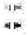
- 1 denotes a circuit board on the upper side of one first copper layer 2 and on the underside thereof a second copper layer 3 are upset.
- the first copper layer 2 is electrical insulating solder resist 4 partially covered.
- the same is the second Copper layer partially covered with the solder resist 4.
- a first one Contact point 5 is circular. It is marginalized by the Solder resist 4 limited.
- the first contact point 5 has a central one Breakthrough 6 on.
- On the top of the board 1 is one second contact point 7 formed, which is also circular through the solder resist 4 is limited.
- the second contact point 7 also has the central breakthrough 6 on.
- the second contact point 7 is additionally coated with a solder 8 here. Lot 8 can e.g. be applied by a printing process.
- connection element 9 With 9 a connection element of a component 10 is designated.
- the Connection element 9 passes through the opening 6. Its free end protrudes the level formed by the first contact point 5 on the underside of the Board 1. Between the connecting element 9 and the inside of the Breakthrough 6, an annular gap 11 is formed.
- the embodiment of Figure 1 is in the soldered state shown.
- the molten solder 12 flows by the action of capillary forces in the annular gap 11 and comes finally in contact with the fixed solder 8, which is on the second Contact point 7 is applied.
- the solder 8 melts as a result of contact with the molten solder 12.
- it can also be caused by direct contact with the connecting element 9 heated by the molten solder 12 melt, then penetrate from above into the annular gap 11 and deal with the unite ascending lot 12. It forms on the second Contact point 7 a Lotmeniskus, which in turn in contact with a Component 10 provided layer of solder 8 comes.
- FIG 3 a forming solder joint is shown, in which the additional application of a solder 8 on the second contact point 7 and the Component 10 has been dispensed with.
- too molten solder is drawn into the annular gap 11 by capillary forces and reaches the second contact point 7.
- the weight of the Component 10 through the formed solder connection directly to the second Contact point 7 removed.
- the method can then be carried out particularly effectively be when the diameter of the further openings 13 and the Gap distance of the annular gap 11 are chosen so that by means of capillary forces the molten solder 12 to the surface of the second contact point 7 is moved.
- To support the movement of the molten solder 12 it is also possible to close the top of the circuit board 1 with a vacuum act upon.
Abstract
Description
Die Erfindung betrifft ein Verfahren zur Herstellung einer Lötverbindung eines Anschlußelements mit einer auf einer Platine vorgesehenen Kontaktstelle. Sie betrifft ferner eine Schaltung.The invention relates to a method for producing a solder connection Connection element with a contact point provided on a circuit board. she also relates to a circuit.
Nach dem Stand der Technik wird eine Lötverbindung von Anschlußelementen mit Kontaktstellen einer Platine üblicherweise im Wellenlötverfahren hergestellt. Dabei wird eine Unterseite der Platine mit schmelzflüssigem Lot beaufschlagt. Das schmelzflüssige Lot haftet an den Kontaktstellen und den diese Kontaktstellen durchgreifenden Anschlußelementen. Die Anschlußelemente werden nach der Erstarrung des Lots elektrisch leitend mit den ersten Kontaktstellen fest verbunden. - Das Eigengewicht des Bauelements wird über die so hergestellte Lötverbindung auf die Platine abgetragen. Im Laufe der Zeit kommt es, bedingt durch Erwärmung oder Erschütterung, spannungsbedingt im Lot zu Veränderungen der Kristallstruktur. Das kann zum Bruch der Lötverbindung führen. Man bezeichnet eine derart gebrochene Lötverbindung auch als "kalte Lötstelle".According to the prior art, a solder connection of connection elements with contact points on a board, usually using wave soldering manufactured. In doing so, an underside of the board with molten solder acted upon. The molten solder adheres to the contact points and the through these contact points connecting elements. The Connection elements become electrically conductive after the solder has solidified the first contact points firmly connected. - The dead weight of the The component is connected to the circuit board using the solder connection worn away. Over time it happens due to warming or Vibration, due to tension in the plumb line to changes in the crystal structure. This can break the solder joint. One is called such broken solder joint also as a "cold solder joint".
Um diesem Nachteil entgegenzuwirken ist man dazu übergegangen, eine Niete im Bereich eines die Kontaktstelle durchgreifenden Durchbruchs vorzusehen. Wegen der für das Lot günstigeren Benetzungseigenschaften des Nietenmaterials wird hier das Lot durch Kapillarkräfte in einen zwischen der Niete und dem Anschlußelement gebildeten Ringspalt gezogen. Die sich ergebende Lötverbindung ist haltbarer. Das Vorsehen einer Niete ist jedoch insbesondere bei stark miniaturisierten Schaltungen sowie Schaltungen mit einer Vielzahl von ersten Kontaktstellen zeit- und kostenaufwendig. In order to counteract this disadvantage, a rivet has been adopted in the area of a breakthrough penetrating the contact point. Because of the more favorable wetting properties of the solder Rivet material is the solder by capillary forces in one between the Rivet and the connecting element formed annular gap pulled. Which resulting solder joint is more durable. However, the provision of a rivet is especially with highly miniaturized circuits and circuits with a large number of first contact points are time-consuming and costly.
Des weiteren ist es bekannt, die Innenwand des Durchbruchs mit Lot zu beschichten. Auch dieses Verfahren führt zu einer haltbareren Lötverbindung. Gleichwohl ist der damit verbundene Kosten- und Zeitaufwand ebenfalls erheblich.Furthermore, it is known to solder the inner wall of the opening coat. This process also leads to a more durable solder joint. Nevertheless, the associated cost and time is also considerably.
Ferner sind nach dem Stand der Technik Platinen bekannt, welche beidseitig mit einer Kupferschicht versehen sind Auf der unteren Seite dient die Kupferschicht zur Herstellung elektrischer Verbindungswege. Die Durchbrüche sind hier unmittelbar von den Kontaktelementen umgeben, selbst aber nicht leitend ummantelt. Auf der Oberseite dient die Kupferschicht üblicherweise nicht zur Herstellung von elektrischen Verbindungswegen, sondern zur Abschirmung. Um die Gefahr einer Fehlkontaktierung zu minimieren, weist die Kupferschicht im Bereich der Durchbrüche Aussparungen auf. Im übrigen ist die auf der Oberseite vorgesehene Kupferschicht mit einem elektrisch isolierenden Lötstoplack überdeckt.Furthermore, boards are known from the prior art, which are on both sides are provided with a copper layer on the lower side Copper layer for the production of electrical connection paths. The breakthroughs are directly surrounded by the contact elements here, but not themselves sheathed in a conductive manner. The copper layer on the top is usually used not for the production of electrical connection paths, but for Shielding. In order to minimize the risk of incorrect contacting, the Copper layer in the area of the cutouts. For the rest is the copper layer provided on the top with an electrical insulating solder resist covered.
Aus JP 11 04 6057 A ist ein Verfahren zur Herstellung einer Lötverbindung eines Anschlusselements mit einer auf einer Platine vorgesehenen Kontaktstelle mit folgenden Schritten bekannt:
- Vorsehen einer ersten Kontaktstelle auf der Unterseite der Platine und einer zweiten Kontaktstelle in gegenüberliegender Anordnung auf der Oberseite der Platine,
- Durchführen des Anschlusselements durch einen die erste und die zweite Kontaktstelle durchgreifenden Durchbruch, so dass das freie Ende des Anschlusselements über eine durch die erste Kontaktstelle beschriebene Ebene hervorsteht und zwischen der Wand des Durchbruchs und dem Anschlusselement ein Ringspalt gebildet ist und
- Aufbringen eines schmelzflüssigen Lots auf die erste Kontaktstelle und das freie Ende des Anschlusselements, so dass das Lot in den Ringspalt eindringt und entlang des Anschlusselements zur zweiten Kontaktstelle (7) fließt und eine Lötverbindung zwischen der ersten und der zweiten (7) Kontaktstelle und dem Anschlusselement (9) gebildet wird.
- Providing a first contact point on the underside of the board and a second contact point in an opposite arrangement on the top side of the board,
- Passing the connection element through an opening penetrating through the first and the second contact point, so that the free end of the connection element protrudes beyond a plane described by the first contact point and an annular gap is formed between the wall of the opening and the connection element and
- Applying a molten solder to the first contact point and the free end of the connection element so that the solder penetrates into the annular gap and flows along the connection element to the second contact point (7) and a solder connection between the first and the second (7) contact point and the connection element (9) is formed.
Aus EP 0 367 076 A ist ein Verfahren zur Durchkontaktierung einer beidseitig kaschierten Leiterplatte bekannt. Hierbei werden über Öffnungen in der Leiterplatte Bauelemente durchgeführt und auf der Unterseite verlötet.From EP 0 367 076 A is a method for through-plating on both sides laminated circuit board known. Here are openings in the Printed circuit board components and soldered on the underside.
Aus DE 3 231 056 A ist ein Verfahren zum Aufbringen von unbedrahteten
Bauelementen auf Leiterplatten bekannt. Hierbei werden Lötflächen an den
Stellen auf der Bauelementseite der Leiterplatte erzeugt, an denen nach dem
Aufbringen der unbedrahteten Bauelemente, deren Anschlüsse aufliegen.
Auf der dazu gegenüberliegenden Stelle der Lötseite der Leiterplatte werden ebenfalls Lötflächen erzeugt. Die die Lötflächen verbindenden Bohrungen sind in die Leiterplatte eingearbeitet, wobei diese Bohrungen anschließend metallisiert werden, wobei zu beachten ist, dass die Bauelemente die Bohrungen beim Aufbringen nicht vollständig bedecken. Anschließend werden die aufgebrachten Bauelemente in einem maschinellen Lötverfahren gelötet.Be on the opposite side of the solder side of the circuit board also created solder pads. The holes that connect the soldering areas are incorporated into the circuit board, these holes then be metallized, whereby it should be noted that the components Do not completely cover holes when applying. Then be the applied components are soldered in a mechanical soldering process.
Aufgabe der Erfindung ist es, die Nachteile nach dem Stand der Technik zu
beseitigen. Es soll insbesondere ein Verfahren angegeben werden, mit dem
auf möglichst einfache und kostengünstige Weise eine haltbare Lötverbindung
hergestellt wird.
Diese Aufgabe wird durch die Merkmale der Ansprüche 1 und 8 gelöst.
Zweckmäßige Ausgestaltungen ergeben sich aus den Merkmalen der
Ansprüche 2 bis 7.The object of the invention is to eliminate the disadvantages of the prior art. In particular, a method is to be specified with which a durable solder connection is produced in the simplest and cheapest possible way.
This object is solved by the features of
Nach Maßgabe der Erfindung ist ein Verfahren zur Herstellung einer
Lötverbindung eines Anschlusselements mit einer auf einer Platine
vorgesehenen Kontaktstelle mit folgenden Schritten vorgesehen:
Mit dem vorgeschlagenen Verfahren kann auf einfache und kostengünstige Weise eine besonders stabile Lötverbindung hergestellt werden. Die Lötverbindung kann unter Verwendung des herkömmlichen Wellenlötverfahrens hergestellt werden. Zu ihrer Realisierung ist es lediglich erforderlich, die Struktur einer an sich bekannten auf der Oberseite von Platinen vorgesehenen Kupfer- und Lötstoplackschicht zu ändern.With the proposed method can be simple and inexpensive How a particularly stable solder joint can be made. The Solder connection can be made using the conventional one Wave soldering process are produced. It is only for their realization required the structure of a known on the top of Change the circuit board provided copper and solder resist layer.
Vorteilhafterweise wird die Spaltbreite des Ringspalts so dimensioniert, daß das Lot durch Kapillarkräfte von der ersten bis zur zweiten Kontaktstelle bewegt wird. Es kann in diesem Fall auf gesonderte Mittel zur Bewegung des Lots von der ersten bis zur zweiten Kontaktstelle verzichtet werden. Bei solchen gesonderten Mitteln kann es sich z.B. um Mittel zur Erzeugung eines auf den Ringspalt wirkenden Unterdrucks handeln. The gap width of the annular gap is advantageously dimensioned such that the solder by capillary forces from the first to the second contact point is moved. In this case, separate means for moving the Lots from the first to the second contact point can be dispensed with. At such separate means may e.g. to generate funds for a act on negative pressure acting on the annular gap.
Nach einem weiteren Ausgestaltungsmerkmal ist vorgesehen, daß vor der Herstellung der Lötverbindung auf die erste und/oder zweite Kontaktstelle eine aus Lot hergestellte Schicht aufgebracht wird. Eine solche Schicht schmilzt besonders leicht bei Kontakt mit dem schmelzflüssigen Lot. Sie kann auf die erste und/oder zweite Kontaktstelle gewalzt oder gedruckt werden.According to a further design feature, it is provided that before the Establish the soldered connection to the first and / or second contact point layer made of solder is applied. Such a layer melts particularly easy on contact with the molten solder. You can on the first and / or second contact point are rolled or printed.
Nach einer weiteren Ausgestaltung kann mindestens ein weiterer die erste mit der zweiten Kontaktstelle verbindender Durchbruch vorgesehen sein. Der Durchmesser des weiteren Durchbruchs ist zweckmäßigerweise so dimensioniert, daß das Lot durch Kapillarkräfte von der ersten zur zweiten Kontaktstelle bewegt wird. Der weitere Durchbruch kann im Randbereich der Kontaktstellen vorgesehen sein. Im Falle des Vorsehens mehrerer weiterer Durchbrüche sind diese vorteilhafterweise kranzartig um den Umfang der Kontaktstellen angeordnet. Die vorgeschlagene Ausgestaltung trägt zu einer besonders schnellen und sicheren Ausbildung der die erste und zweite Kontaktstelle verbindenden Lötbrücke bei.According to a further embodiment, at least one other can use the first one breakthrough connecting the second contact point may be provided. The The diameter of the further opening is expediently so dimensioned that the solder by capillary forces from the first to the second Contact point is moved. The further breakthrough can be in the marginal area of the Contact points may be provided. In the case of the provision of several more Breakthroughs are advantageously ring-shaped around the circumference of the Contact points arranged. The proposed design contributes to a particularly quick and safe training of the first and second Contact point connecting solder bridge.
Desweiteren hat es sich als vorteilhaft erwiesen, ein mit dem Anschlußelement verbundenes Bauelement in der Nähe der zweiten Kontaktstelle derart anzuordnen, daß das Lot das Bauelement mit der zweiten Kontaktstelle verbindet. In diesem Fall wird das Eigengewicht des Bauelements unmittelbar auf die auf der Oberseite der Platine angeordnete zweite Kontaktstelle abgetragen. Damit wird besonders effektiv einem Bruch der Lötstelle entgegengewirkt. Um die vorgenannte Lötverbindung möglichst zuverlässig herzustellen, ist es zweckmäßig, das Bauelement vor der Montage zumindest abschnittsweise mit dem Lot zu beschichten.Furthermore, it has proven to be advantageous to use the connecting element connected component in the vicinity of the second contact point in such a way to arrange that the solder the component with the second contact point connects. In this case, the weight of the component becomes immediate on the second contact point arranged on the top of the board worn away. This makes breaking the solder joint particularly effective counteracted. To make the aforementioned soldered connection as reliable as possible To manufacture, it is expedient to at least the component before assembly to be coated in sections with the solder.
Nachfolgend werden anhand der Zeichnungen Ausführungsbeispiele der Erfindung näher erläutert. Es zeigen:
- Fig.1
- einen schematischen Querschnitt eines ersten Ausführungsbeispiels,
- Fig.2
- das Ausführungsbeispiel nach Fig.1 im verlöteten Zustand,
- Fig.3
- eine Querschnittsansicht eines zweiten Ausführungsbeispiels im verlöteten Zustand und
- Fig.4
- eine Querschnittsansicht eines dritten Ausführungsbeispiels im verlöteten Zustand.
- Fig. 1
- 2 shows a schematic cross section of a first exemplary embodiment,
- Fig. 2
- 1 in the soldered state,
- Fig. 3
- a cross-sectional view of a second embodiment in the soldered state and
- Fig. 4
- a cross-sectional view of a third embodiment in the soldered state.
In den Fig.1 bis 4 ist mit 1 eine Platine bezeichnet auf deren Oberseite eine
erste Kupferschicht 2 und auf deren Unterseite eine zweite Kupferschicht 3
aufgebracht sind. Die erste Kupferschicht 2 ist mit einem elektrisch
isolierenden Lötstoplack 4 teilweise überdeckt. Desgleichen ist auch die zweite
Kupferschicht teilweise mit dem Lötstoplack 4 überdeckt. Eine erste
Kontaktstelle 5 ist kreisförmig ausgebildet. Sie wird randlich durch den
Lötstoplack 4 begrenzt. Die erste Kontaktstelle 5 weist einen zentralen
Durchbruch 6 auf. In ähnlicher Weise ist auf der Oberseite der Platine 1 eine
zweite Kontaktstelle 7 gebildet, die ebenfalls kreisförmig durch den Lötstoplack
4 begrenzt ist. Auch die zweite Kontaktstelle 7 weist den zentralen Durchbruch
6 auf. Die zweite Kontaktstelle 7 ist hier zusätzlich mit einem Lot 8 beschichtet.
Das Lot 8 kann z.B. durch ein Druckverfahren aufgebracht werden.1 to 4, 1 denotes a circuit board on the upper side of one
Mit 9 ist ein Anschlußelement eines Bauelements 10 bezeichnet. Das
Anschlußelement 9 durchgreift den Durchbruch 6. Sein freies Ende ragt über
die durch die erste Kontaktstelle 5 gebildete Ebene an der Unterseite der
Platine 1 hervor. Zwischen dem Anschlußelement 9 und der Innenseite des
Durchbruchs 6 ist ein Ringspalt 11 gebildet. With 9 a connection element of a
In Fig.2 ist das Ausführungsbeispiel gemäß Fig.1 im verlöteten Zustand
gezeigt. Z.B. im Wellenlötverfahren wird das freie Ende des Anschlußelements
9 mit schmelzflüssigem Lot 12 beaufschlagt. Das schmelzflüssige Lot 12 fließt
durch die Wirkung von Kapillarkräften in den Ringspalt 11 und kommt
schließlich mit dem festen Lot 8 in Kontakt, welches auf der zweiten
Kontaktstelle 7 aufgebracht ist. Das Lot 8 schmilzt infolge des Kontakts mit dem
schmelzflüssigen Lot 12. Es kann aber auch durch unmittelbaren Kontakt mit
dem durch das schmelzflüssige Lot 12 erhitzten Anschlußelement 9
schmelzen, dann von oben in den Ringspalt 11 eindringen und sich mit dem
darin aufsteigenden Lot 12 vereinigen. Es bildet sich auf der zweiten
Kontaktstelle 7 eine Lotmeniskus, der wiederum in Kontakt mit einer am
Bauelement 10 vorgesehen Schicht des Lots 8 kommt. Dadurch wird auch
diese Schicht geschmolzen. Es bildet sich insgesamt eine komplexe
Lötverbindung zwischen der ersten Kontaktstelle 5, der zweiten Kontaktstelle 7,
dem Anschlußelement 9 und dem Bauelement 10 aus. Wie aus Fig.2 deutlich
erkennbar ist, wird das Eigengewicht des Bauelements 10 unmittelbar auf die
zweite Kontaktstelle 7 abgetragen. Die so hergestellte Lötverbindung ist
besonders dauerhaft. Das Risiko eines Bruchs einer solchen Lötverbindung ist
minimal.In Figure 2, the embodiment of Figure 1 is in the soldered state
shown. For example, in the wave soldering process, the free end of the
In Fig.3 ist eine sich ausbildende Lötverbindung gezeigt, bei der auf das
zusätzliche Aufbringen eines Lots 8 auf die zweite Kontaktstelle 7 sowie das
Bauelement 10 verzichtet worden ist. Auch in diesem Fall wird das
schmelzflüssige Lot durch Kapillarkräfte in den Ringspalt 11 gezogen und
gelangt bis zur zweiten Kontaktstelle 7. Auch hier wird das Eigengewicht des
Bauelements 10 durch die gebildete Lötverbindung unmittelbar auf die zweite
Kontaktstelle 7 abgetragen.In Figure 3, a forming solder joint is shown, in which the
additional application of a
Bei dem in Fig.4 im schematischen Querschnitt gezeigten Ausführungsbeispiel
sind weitere Durchbrüche 13 vorgesehen, welche die Platine 1 sowie die erste
5 und die zweite Kontaktstelle 7 randlich durchgreifen. Beim Aufbringen des
schmelzflüssigen Lots 12 auf die erste Kontaktstelle 5 wird dieses sowohl
durch den Ringspalt 11 als auch durch die weiteren Durchbrüche 13 durch
Kapillarkräfte bis auf die zweite Kontaktstelle 7 gezogen. Es bildet sich ein
Lötminiskus im Bereich der zweiten Kontaktstelle 7 aus. Die so hergestellte
Lötstelle ist besonders stabil.In the embodiment shown in Figure 4 in schematic cross section
Das Verfahren kann insbesondere dann besonders effektiv durchgeführt
werden, wenn der Durchmesser der weiteren Durchbrüche 13 sowie der
Spaltabstand des Ringspalts 11 so gewählt sind, daß mittels Kapillarkräften
das schmelzflüssige Lot 12 bis zur Oberfläche der zweiten Kontaktstelle 7
bewegt wird. Um die Bewegung des schmelzflüssigen Lots 12 zu unterstützen
ist es aber auch möglich, die Oberseite der Platine 1 mit einem Unterdruck zu
beaufschlagen. The method can then be carried out particularly effectively
be when the diameter of the
- 11
- Platinecircuit board
- 22nd
- erste Kupferschichtfirst copper layer
- 33rd
- zweite Kupferschichtsecond copper layer
- 44th
- LötstoplackSolder resist
- 55
- erste Kontaktstellefirst contact point
- 66
- Durchbruchbreakthrough
- 77
- zweite Kontaktstellesecond contact point
- 88th
- LötschichtSolder layer
- 99
- AnschlußelementConnector
- 1010th
- BauelementComponent
- 1111
- RingspaltAnnular gap
- 1212th
- schmelzflüssiges Lotmolten solder
- 1313
- weiterer Durchbruchfurther breakthrough
Claims (9)
ein mit dem Anschlusselement (9) verbundenes Bauelement (10) in der Nähe der zweiten Kontaktstelle (7) derart angeordnet wird, dass das Lot (12) das Bauelement (10) mit der zweiten Kontaktstelle (7) verbindet. Method for producing a soldered connection of a connection element (9) with a contact point (5, 7) provided on the circuit board (1) with the following steps:
a component (10) connected to the connection element (9) is arranged in the vicinity of the second contact point (7) such that the solder (12) connects the component (10) to the second contact point (7).
Applications Claiming Priority (2)
| Application Number | Priority Date | Filing Date | Title |
|---|---|---|---|
| DE19963108A DE19963108C1 (en) | 1999-12-24 | 1999-12-24 | Method for producing a solder connection and circuit with such a solder connection |
| DE19963108 | 1999-12-24 |
Publications (3)
| Publication Number | Publication Date |
|---|---|
| EP1111974A2 true EP1111974A2 (en) | 2001-06-27 |
| EP1111974A3 EP1111974A3 (en) | 2003-05-14 |
| EP1111974B1 EP1111974B1 (en) | 2007-10-31 |
Family
ID=7934572
Family Applications (1)
| Application Number | Title | Priority Date | Filing Date |
|---|---|---|---|
| EP00127521A Expired - Lifetime EP1111974B1 (en) | 1999-12-24 | 2000-12-15 | Process for manufacturing a solder connection |
Country Status (3)
| Country | Link |
|---|---|
| EP (1) | EP1111974B1 (en) |
| AT (1) | ATE377344T1 (en) |
| DE (2) | DE19963108C1 (en) |
Families Citing this family (2)
| Publication number | Priority date | Publication date | Assignee | Title |
|---|---|---|---|---|
| DE10331840A1 (en) * | 2003-07-14 | 2005-02-24 | Rosenberger Hochfrequenztechnik Gmbh & Co. Kg | Component for a printed circuit board and method for assembling the printed circuit board with this component |
| CN114485597B (en) * | 2022-02-10 | 2022-12-09 | 南通天正信息技术服务有限公司 | Projection point-to-point measurement plumb device and processing device thereof |
Citations (9)
| Publication number | Priority date | Publication date | Assignee | Title |
|---|---|---|---|---|
| CH375051A (en) * | 1959-10-14 | 1964-02-15 | Schweiz Wagons Aufzuegefab | Process for producing electrically conductive soldered connections in printed circuits |
| US3500538A (en) * | 1966-08-29 | 1970-03-17 | Gen Electric | Method for producing a wire having improved soldering characteristics |
| DE2657313A1 (en) * | 1976-12-17 | 1978-06-22 | Siemens Ag | Circuit board or contact support - has holes in which component leads or pins are placed and subsequently dip soldered |
| US4477970A (en) * | 1982-04-01 | 1984-10-23 | Motorola, Inc. | P.C. Board mounting method for surface mounted components |
| JPS6437073A (en) * | 1987-08-03 | 1989-02-07 | Sony Corp | Printed board |
| JPH057077A (en) * | 1991-04-26 | 1993-01-14 | Matsushita Electric Works Ltd | Soldering method |
| EP0594408A1 (en) * | 1992-10-19 | 1994-04-27 | Nippon Cmk Corp. | A connection device for a printed wiring board |
| JPH10335775A (en) * | 1997-05-29 | 1998-12-18 | Fuji Electric Co Ltd | Printed circuit board |
| JPH11251733A (en) * | 1998-02-27 | 1999-09-17 | Fuji Xerox Co Ltd | Method for mounting lead component on printed board |
Family Cites Families (2)
| Publication number | Priority date | Publication date | Assignee | Title |
|---|---|---|---|---|
| DE3231056A1 (en) * | 1982-08-20 | 1984-02-23 | Siemens AG, 1000 Berlin und 8000 München | Method for fitting unwired components on to printed circuit boards |
| FI84413C (en) * | 1988-10-27 | 1991-11-25 | Salora Oy | GENOMFOERING FOER ATT DUBBELSIDIGT KRETSKORT SAMT FOERFARANDE FOER AOSTADKOMMANDE AV DENSAMMA. |
-
1999
- 1999-12-24 DE DE19963108A patent/DE19963108C1/en not_active Expired - Fee Related
-
2000
- 2000-12-15 EP EP00127521A patent/EP1111974B1/en not_active Expired - Lifetime
- 2000-12-15 AT AT00127521T patent/ATE377344T1/en not_active IP Right Cessation
- 2000-12-15 DE DE50014742T patent/DE50014742D1/en not_active Expired - Fee Related
Patent Citations (9)
| Publication number | Priority date | Publication date | Assignee | Title |
|---|---|---|---|---|
| CH375051A (en) * | 1959-10-14 | 1964-02-15 | Schweiz Wagons Aufzuegefab | Process for producing electrically conductive soldered connections in printed circuits |
| US3500538A (en) * | 1966-08-29 | 1970-03-17 | Gen Electric | Method for producing a wire having improved soldering characteristics |
| DE2657313A1 (en) * | 1976-12-17 | 1978-06-22 | Siemens Ag | Circuit board or contact support - has holes in which component leads or pins are placed and subsequently dip soldered |
| US4477970A (en) * | 1982-04-01 | 1984-10-23 | Motorola, Inc. | P.C. Board mounting method for surface mounted components |
| JPS6437073A (en) * | 1987-08-03 | 1989-02-07 | Sony Corp | Printed board |
| JPH057077A (en) * | 1991-04-26 | 1993-01-14 | Matsushita Electric Works Ltd | Soldering method |
| EP0594408A1 (en) * | 1992-10-19 | 1994-04-27 | Nippon Cmk Corp. | A connection device for a printed wiring board |
| JPH10335775A (en) * | 1997-05-29 | 1998-12-18 | Fuji Electric Co Ltd | Printed circuit board |
| JPH11251733A (en) * | 1998-02-27 | 1999-09-17 | Fuji Xerox Co Ltd | Method for mounting lead component on printed board |
Non-Patent Citations (4)
| Title |
|---|
| PATENT ABSTRACTS OF JAPAN vol. 013, no. 230 (E-764), 26. Mai 1989 (1989-05-26) -& JP 01 037073 A (SONY CORP), 7. Februar 1989 (1989-02-07) * |
| PATENT ABSTRACTS OF JAPAN vol. 017, no. 264 (E-1370), 24. Mai 1993 (1993-05-24) -& JP 05 007077 A (MATSUSHITA ELECTRIC WORKS LTD), 14. Januar 1993 (1993-01-14) * |
| PATENT ABSTRACTS OF JAPAN vol. 1999, no. 03, 31. März 1999 (1999-03-31) -& JP 10 335775 A (FUJI ELECTRIC CO LTD), 18. Dezember 1998 (1998-12-18) * |
| PATENT ABSTRACTS OF JAPAN vol. 1999, no. 14, 22. Dezember 1999 (1999-12-22) -& JP 11 251733 A (FUJI XEROX CO LTD), 17. September 1999 (1999-09-17) * |
Also Published As
| Publication number | Publication date |
|---|---|
| EP1111974B1 (en) | 2007-10-31 |
| EP1111974A3 (en) | 2003-05-14 |
| DE50014742D1 (en) | 2007-12-13 |
| DE19963108C1 (en) | 2001-06-21 |
| ATE377344T1 (en) | 2007-11-15 |
Similar Documents
| Publication | Publication Date | Title |
|---|---|---|
| DE2852753C3 (en) | Method for fastening components with flat connection contacts on a printed circuit board and template for carrying out the method | |
| EP0301533A2 (en) | Electric fuse and method for its manufacture | |
| EP2516321B1 (en) | Sensor comprising a preferably multilayered ceramic substrate and method for producing it | |
| DE19809138A1 (en) | Printed circuit board with SMD components | |
| DE69429293T2 (en) | Car window glass with a printed conductor structure | |
| EP0166105B1 (en) | Flexible board and process for making it | |
| WO2011107547A1 (en) | Electrical contact arrangement | |
| EP1665914B1 (en) | Printed circuit board comprising a holding device for retaining wired electronic components, method for the production of such a printed circuit board, and use thereof in a soldering furnace | |
| EP3817881B1 (en) | Method for manufacturing a high temperature resistant lead-free solder connection and arrangement with a high temperature resistant lead-free solder connection | |
| EP1080615B1 (en) | Multiple printed panel for electronics components, and method for constructing bumps, soldering frames, spacers and similar on said multiple printed panel. | |
| EP1393604A1 (en) | Printed circuit board comprising a contact sleeve that is mounted thereon | |
| EP1940207A2 (en) | Electric device with a carrier element with a minimum of one special connecting surface and a component mounted on the surface | |
| EP0710432B1 (en) | Process for manufacturing printed circuit foils or semifinished products for printed circuit foils, and thus manufactured printed circuit foils and semifinished products | |
| DE10045534A1 (en) | Electronic component has capillary elements as connection elements, which are connected with contact areas of a carrier | |
| DE19963108C1 (en) | Method for producing a solder connection and circuit with such a solder connection | |
| DE112015003374T5 (en) | circuitry | |
| WO2004086831A2 (en) | Method and device for electrically and mechanically connecting two printed boards | |
| DE102015102505B4 (en) | circuit board | |
| DE10064221B4 (en) | Printed circuit board with cooled SMD component | |
| DE2820002A1 (en) | Terminal for circuit board - has connecting wires pushed in holes in board with grooves and collars at their tops | |
| EP0144413A1 (en) | Printed board for the surface soldering of integrated miniature circuits and manufacturing method of such printed boards | |
| DE102019129971A1 (en) | Method for soldering a component onto a printed circuit board, electronic unit and field device in automation technology | |
| EP0298410A1 (en) | Electrical component with contact pins | |
| DE4208594A1 (en) | Prefabricated electrical component fixing to PCB - serially mfg. unitary circuits for selective imposition on regions of circuit board requiring rectification or extension | |
| DE19814428B4 (en) | Printed circuit board with large contact pads (solder pads) provided with solder deposits |
Legal Events
| Date | Code | Title | Description |
|---|---|---|---|
| PUAI | Public reference made under article 153(3) epc to a published international application that has entered the european phase |
Free format text: ORIGINAL CODE: 0009012 |
|
| AK | Designated contracting states |
Kind code of ref document: A2 Designated state(s): AT BE CH CY DE DK ES FI FR GB GR IE IT LI LU MC NL PT SE TR |
|
| AX | Request for extension of the european patent |
Free format text: AL;LT;LV;MK;RO;SI |
|
| PUAL | Search report despatched |
Free format text: ORIGINAL CODE: 0009013 |
|
| AK | Designated contracting states |
Designated state(s): AT BE CH CY DE DK ES FI FR GB GR IE IT LI LU MC NL PT SE TR |
|
| AX | Request for extension of the european patent |
Extension state: AL LT LV MK RO SI |
|
| 17P | Request for examination filed |
Effective date: 20031029 |
|
| AKX | Designation fees paid |
Designated state(s): AT BE CH CY DE DK ES FI FR GB GR IE IT LI LU MC NL PT SE TR |
|
| RAP1 | Party data changed (applicant data changed or rights of an application transferred) |
Owner name: GRUNDIG MULTIMEDIA B.V. |
|
| GRAP | Despatch of communication of intention to grant a patent |
Free format text: ORIGINAL CODE: EPIDOSNIGR1 |
|
| GRAS | Grant fee paid |
Free format text: ORIGINAL CODE: EPIDOSNIGR3 |
|
| GRAA | (expected) grant |
Free format text: ORIGINAL CODE: 0009210 |
|
| AK | Designated contracting states |
Kind code of ref document: B1 Designated state(s): AT BE CH CY DE DK ES FI FR GB GR IE IT LI LU MC NL PT SE TR |
|
| REG | Reference to a national code |
Ref country code: GB Ref legal event code: FG4D Free format text: NOT ENGLISH |
|
| REG | Reference to a national code |
Ref country code: IE Ref legal event code: FG4D Free format text: LANGUAGE OF EP DOCUMENT: GERMAN |
|
| REG | Reference to a national code |
Ref country code: CH Ref legal event code: EP |
|
| REF | Corresponds to: |
Ref document number: 50014742 Country of ref document: DE Date of ref document: 20071213 Kind code of ref document: P |
|
| NLV1 | Nl: lapsed or annulled due to failure to fulfill the requirements of art. 29p and 29m of the patents act | ||
| PG25 | Lapsed in a contracting state [announced via postgrant information from national office to epo] |
Ref country code: SE Free format text: LAPSE BECAUSE OF FAILURE TO SUBMIT A TRANSLATION OF THE DESCRIPTION OR TO PAY THE FEE WITHIN THE PRESCRIBED TIME-LIMIT Effective date: 20080131 Ref country code: NL Free format text: LAPSE BECAUSE OF FAILURE TO SUBMIT A TRANSLATION OF THE DESCRIPTION OR TO PAY THE FEE WITHIN THE PRESCRIBED TIME-LIMIT Effective date: 20071031 Ref country code: ES Free format text: LAPSE BECAUSE OF FAILURE TO SUBMIT A TRANSLATION OF THE DESCRIPTION OR TO PAY THE FEE WITHIN THE PRESCRIBED TIME-LIMIT Effective date: 20080211 |
|
| GBV | Gb: ep patent (uk) treated as always having been void in accordance with gb section 77(7)/1977 [no translation filed] | ||
| PG25 | Lapsed in a contracting state [announced via postgrant information from national office to epo] |
Ref country code: PT Free format text: LAPSE BECAUSE OF FAILURE TO SUBMIT A TRANSLATION OF THE DESCRIPTION OR TO PAY THE FEE WITHIN THE PRESCRIBED TIME-LIMIT Effective date: 20080331 |
|
| REG | Reference to a national code |
Ref country code: IE Ref legal event code: FD4D |
|
| BERE | Be: lapsed |
Owner name: GRUNDIG MULTIMEDIA B.V. Effective date: 20071231 |
|
| PG25 | Lapsed in a contracting state [announced via postgrant information from national office to epo] |
Ref country code: MC Free format text: LAPSE BECAUSE OF NON-PAYMENT OF DUE FEES Effective date: 20071231 Ref country code: DK Free format text: LAPSE BECAUSE OF FAILURE TO SUBMIT A TRANSLATION OF THE DESCRIPTION OR TO PAY THE FEE WITHIN THE PRESCRIBED TIME-LIMIT Effective date: 20071031 |
|
| REG | Reference to a national code |
Ref country code: CH Ref legal event code: PL |
|
| EN | Fr: translation not filed | ||
| PLBE | No opposition filed within time limit |
Free format text: ORIGINAL CODE: 0009261 |
|
| STAA | Information on the status of an ep patent application or granted ep patent |
Free format text: STATUS: NO OPPOSITION FILED WITHIN TIME LIMIT |
|
| PG25 | Lapsed in a contracting state [announced via postgrant information from national office to epo] |
Ref country code: BE Free format text: LAPSE BECAUSE OF NON-PAYMENT OF DUE FEES Effective date: 20071231 |
|
| 26N | No opposition filed |
Effective date: 20080801 |
|
| PG25 | Lapsed in a contracting state [announced via postgrant information from national office to epo] |
Ref country code: IE Free format text: LAPSE BECAUSE OF FAILURE TO SUBMIT A TRANSLATION OF THE DESCRIPTION OR TO PAY THE FEE WITHIN THE PRESCRIBED TIME-LIMIT Effective date: 20071031 Ref country code: LI Free format text: LAPSE BECAUSE OF NON-PAYMENT OF DUE FEES Effective date: 20071231 Ref country code: CH Free format text: LAPSE BECAUSE OF NON-PAYMENT OF DUE FEES Effective date: 20071231 Ref country code: FR Free format text: LAPSE BECAUSE OF FAILURE TO SUBMIT A TRANSLATION OF THE DESCRIPTION OR TO PAY THE FEE WITHIN THE PRESCRIBED TIME-LIMIT Effective date: 20080704 Ref country code: DE Free format text: LAPSE BECAUSE OF NON-PAYMENT OF DUE FEES Effective date: 20080701 |
|
| PG25 | Lapsed in a contracting state [announced via postgrant information from national office to epo] |
Ref country code: GB Free format text: LAPSE BECAUSE OF FAILURE TO SUBMIT A TRANSLATION OF THE DESCRIPTION OR TO PAY THE FEE WITHIN THE PRESCRIBED TIME-LIMIT Effective date: 20071031 |
|
| PG25 | Lapsed in a contracting state [announced via postgrant information from national office to epo] |
Ref country code: GR Free format text: LAPSE BECAUSE OF FAILURE TO SUBMIT A TRANSLATION OF THE DESCRIPTION OR TO PAY THE FEE WITHIN THE PRESCRIBED TIME-LIMIT Effective date: 20080201 |
|
| PG25 | Lapsed in a contracting state [announced via postgrant information from national office to epo] |
Ref country code: FI Free format text: LAPSE BECAUSE OF FAILURE TO SUBMIT A TRANSLATION OF THE DESCRIPTION OR TO PAY THE FEE WITHIN THE PRESCRIBED TIME-LIMIT Effective date: 20071031 |
|
| PG25 | Lapsed in a contracting state [announced via postgrant information from national office to epo] |
Ref country code: AT Free format text: LAPSE BECAUSE OF NON-PAYMENT OF DUE FEES Effective date: 20071215 |
|
| PG25 | Lapsed in a contracting state [announced via postgrant information from national office to epo] |
Ref country code: CY Free format text: LAPSE BECAUSE OF FAILURE TO SUBMIT A TRANSLATION OF THE DESCRIPTION OR TO PAY THE FEE WITHIN THE PRESCRIBED TIME-LIMIT Effective date: 20071031 |
|
| PG25 | Lapsed in a contracting state [announced via postgrant information from national office to epo] |
Ref country code: LU Free format text: LAPSE BECAUSE OF NON-PAYMENT OF DUE FEES Effective date: 20071215 |
|
| PG25 | Lapsed in a contracting state [announced via postgrant information from national office to epo] |
Ref country code: TR Free format text: LAPSE BECAUSE OF FAILURE TO SUBMIT A TRANSLATION OF THE DESCRIPTION OR TO PAY THE FEE WITHIN THE PRESCRIBED TIME-LIMIT Effective date: 20071031 |
|
| PG25 | Lapsed in a contracting state [announced via postgrant information from national office to epo] |
Ref country code: IT Free format text: LAPSE BECAUSE OF NON-PAYMENT OF DUE FEES Effective date: 20071231 |