EP1111688A1 - Diode schottky sur substrat de carbure de silicium - Google Patents
Diode schottky sur substrat de carbure de silicium Download PDFInfo
- Publication number
- EP1111688A1 EP1111688A1 EP00410163A EP00410163A EP1111688A1 EP 1111688 A1 EP1111688 A1 EP 1111688A1 EP 00410163 A EP00410163 A EP 00410163A EP 00410163 A EP00410163 A EP 00410163A EP 1111688 A1 EP1111688 A1 EP 1111688A1
- Authority
- EP
- European Patent Office
- Prior art keywords
- type
- epitaxial layer
- silicon carbide
- trench
- diode
- Prior art date
- Legal status (The legal status is an assumption and is not a legal conclusion. Google has not performed a legal analysis and makes no representation as to the accuracy of the status listed.)
- Granted
Links
Images
Classifications
-
- H—ELECTRICITY
- H10—SEMICONDUCTOR DEVICES; ELECTRIC SOLID-STATE DEVICES NOT OTHERWISE PROVIDED FOR
- H10D—INORGANIC ELECTRIC SEMICONDUCTOR DEVICES
- H10D8/00—Diodes
- H10D8/01—Manufacture or treatment
- H10D8/051—Manufacture or treatment of Schottky diodes
-
- H—ELECTRICITY
- H10—SEMICONDUCTOR DEVICES; ELECTRIC SOLID-STATE DEVICES NOT OTHERWISE PROVIDED FOR
- H10D—INORGANIC ELECTRIC SEMICONDUCTOR DEVICES
- H10D62/00—Semiconductor bodies, or regions thereof, of devices having potential barriers
- H10D62/10—Shapes, relative sizes or dispositions of the regions of the semiconductor bodies; Shapes of the semiconductor bodies
- H10D62/102—Constructional design considerations for preventing surface leakage or controlling electric field concentration
- H10D62/103—Constructional design considerations for preventing surface leakage or controlling electric field concentration for increasing or controlling the breakdown voltage of reverse-biased devices
- H10D62/104—Constructional design considerations for preventing surface leakage or controlling electric field concentration for increasing or controlling the breakdown voltage of reverse-biased devices having particular shapes of the bodies at or near reverse-biased junctions, e.g. having bevels or moats
-
- H—ELECTRICITY
- H10—SEMICONDUCTOR DEVICES; ELECTRIC SOLID-STATE DEVICES NOT OTHERWISE PROVIDED FOR
- H10D—INORGANIC ELECTRIC SEMICONDUCTOR DEVICES
- H10D62/00—Semiconductor bodies, or regions thereof, of devices having potential barriers
- H10D62/10—Shapes, relative sizes or dispositions of the regions of the semiconductor bodies; Shapes of the semiconductor bodies
- H10D62/102—Constructional design considerations for preventing surface leakage or controlling electric field concentration
- H10D62/103—Constructional design considerations for preventing surface leakage or controlling electric field concentration for increasing or controlling the breakdown voltage of reverse-biased devices
- H10D62/105—Constructional design considerations for preventing surface leakage or controlling electric field concentration for increasing or controlling the breakdown voltage of reverse-biased devices by having particular doping profiles, shapes or arrangements of PN junctions; by having supplementary regions, e.g. junction termination extension [JTE]
- H10D62/106—Constructional design considerations for preventing surface leakage or controlling electric field concentration for increasing or controlling the breakdown voltage of reverse-biased devices by having particular doping profiles, shapes or arrangements of PN junctions; by having supplementary regions, e.g. junction termination extension [JTE] having supplementary regions doped oppositely to or in rectifying contact with regions of the semiconductor bodies, e.g. guard rings with PN or Schottky junctions
-
- H—ELECTRICITY
- H10—SEMICONDUCTOR DEVICES; ELECTRIC SOLID-STATE DEVICES NOT OTHERWISE PROVIDED FOR
- H10D—INORGANIC ELECTRIC SEMICONDUCTOR DEVICES
- H10D8/00—Diodes
- H10D8/60—Schottky-barrier diodes
-
- H—ELECTRICITY
- H10—SEMICONDUCTOR DEVICES; ELECTRIC SOLID-STATE DEVICES NOT OTHERWISE PROVIDED FOR
- H10D—INORGANIC ELECTRIC SEMICONDUCTOR DEVICES
- H10D62/00—Semiconductor bodies, or regions thereof, of devices having potential barriers
- H10D62/80—Semiconductor bodies, or regions thereof, of devices having potential barriers characterised by the materials
- H10D62/83—Semiconductor bodies, or regions thereof, of devices having potential barriers characterised by the materials being Group IV materials, e.g. B-doped Si or undoped Ge
- H10D62/832—Semiconductor bodies, or regions thereof, of devices having potential barriers characterised by the materials being Group IV materials, e.g. B-doped Si or undoped Ge being Group IV materials comprising two or more elements, e.g. SiGe
- H10D62/8325—Silicon carbide
Definitions
- the present invention relates to the production of a Schottky diode.
- silicon carbide is a preferable because silicon carbide can withstand voltages per unit of thickness about 10 times higher than silicon.
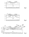
- FIG. 1 The elementary structure of a Schottky diode is illustrated in Figure 1.
- This diode is made from a heavily doped N-type substrate 1 on which a N-type epitaxial layer 2 suitably doped to have the Schottky threshold desired.
- N On this epitaxial layer N is deposited silicon oxide 3 delimiting a window in which one wants to establish Schottky contact through metallization 4.
- the rear side of the component is coated with a metallization 5.
- Such a structure has very poor tensile strength.
- the equipotentials tend to bend to go up towards the surface and this results, in particular in the zones of curvature of the equipotentials, of very strong field variations which limit the possible resistance to reverse voltage.
- the structure shown in FIG. 2 is conventionally used in the field of silicon-based components in which a peripheral ring 6 of type P is formed at the periphery of the area of the Schottky diode. It follows that the equipotentials must pass in volume under the regions P and therefore have a less marked curvature.
- the voltage withstand of the diode is considerably improved. For example, with silicon with a doping level of 10 16 at./cm 3 , there will be a voltage withstand of the order of 10 V without guard ring and of the order of 50 V with ring on call.
- the present invention aims to provide a structure of Schottky diode compatible with manufacturing processes simple silicon carbide and which allows a resistance in relatively high tension.
- the present invention provides a vertical Schottky diode comprising a layer of N-type silicon carbide with low doping level formed by epitaxy on a high level silicon carbide substrate doping, in which the periphery of the active area of the diode is coated with an epitaxial layer of silicon carbide type P; a trench crosses the type P epitaxial layer and penetrates at least part of the layer height epitaxial type N beyond the periphery of the active area; the doping level of the P-type epitaxial layer is chosen so that for the maximum voltage that the diode is likely to support, the equipotentials corresponding to approximately 1/4 to 3/4 of the maximum tension extends to the trench.
- the doping level of the P-type epitaxial layer is slightly higher than the doping of the type N epitaxial layer
- the distance between the external periphery of the active area and the internal periphery of the trench is of the order of 30 to 60 ⁇ m .
- the present invention also relates to a manufacturing process of a vertical Schottky diode on a carbide substrate of heavily N-doped silicon, comprising the steps of forming a lightly doped N-type epitaxial layer; forming a P-type doped epitaxial layer; dig a trench peripheral; depositing an insulating layer; form an opening central through the insulating layer, the epitaxial layer of type P and the epitaxial layer of type N; and drop a metal likely to form a Schottky barrier with the epitaxial layer type N.
- the doping level of the P-type epitaxial layer is chosen so that for the maximum voltage that the diode is likely to support, the equipotentials corresponding to approximately 1/4 to 3/4 of the maximum tension extends to the trench.
- the Schottky diode of FIG. 3 is formed from a plate of heavily-doped silicon carbide 11 of type N.
- the dopant of type N is for example nitrogen.
- On the wafer 11 is formed a thin epitaxial layer 12 of type N more lightly doped. For a desired voltage withstand of the order of 600 to 1000 V, this epitaxial layer will have a thickness of the order of 3 to 6 ⁇ m .
- the Schottky contact is formed between this layer 12 and a metallization 14, for example a silicide of platinum, titanium or nickel or the like.
- the rear face of the plate 11 is coated with a metallization 5 corresponding to the cathode of the diode.
- the distance between the Schottky contact periphery and the trench is of the order of 30 to 60 ⁇ m , for example 40 ⁇ m .
- the doping of the P-type region 15 is chosen for that when a voltage close to the maximum voltage that must support the diode in reverse is applied to it, the equipotentials instead of going all up to the surface extend at least partially up to the area of trench 16.
- the equipotentials instead of going all up to the surface extend at least partially up to the area of trench 16.
- equipotential corresponding to four equally distributed values potential for example values close to 200, 400, 600 and 800 V. It will be noted that the equipotential corresponding substantially at 600 V reaches the trench.
- the way in which the field lines are distributed will depend essentially on the level of doping of the P-type epitaxial layer which on the other hand may be very thin and have a thickness of the order of 1 to 3 ⁇ m .
- a structure is preferred. corresponding to the second case. Indeed, if all the equipotentials go back to the surface or if all the equipotentials go up to the trench, it is necessary that the insulation deposited in surface (commonly silicon oxide) has a particularly good tensile strength, i.e. be deposited with particularly important quality constraints to be able to resist the intense transverse fields which are applied to it.
Landscapes
- Electrodes Of Semiconductors (AREA)
Abstract
Description
Claims (5)
- Diode Schottky verticale comprenant une couche de carbure de silicium (12) de type N à faible niveau de dopage formée par épitaxie sur un substrat de carbure de silicium (11) à fort niveau de dopage, caractérisée en ce que :la périphérie de la zone active de la diode est revêtue d'une couche épitaxiée (15) de carbure de silicium de type P ;une tranchée (16) traverse la couche épitaxiée de type P et la couche épitaxiée de type N au-delà de la périphérie de la zone active ;le niveau de dopage de la couche épitaxiée de type P est choisi pour que, pour la tension maximale que la diode est susceptible de supporter, les équipotentielles correspondant à environ 1/4 à 3/4 de la tension maximale se prolongent jusqu'à la tranchée.
- Diode Schottky selon la revendication 1, caractérisée en ce que le niveau de dopage de la couche épitaxiée de type P est légèrement supérieur au dopage de la couche épitaxiée de type N.
- Diode Schottky selon la revendication 1 ou 2, caractérisée en ce que la distance entre la périphérie externe de la zone active et la périphérie interne de la tranchée est de l'ordre de 30 à 60 µm.
- Procédé de fabrication d'une diode Schottky verticale sur un substrat (11) de carbure de silicium fortement dopé de type N, caractérisé en ce qu'il comprend les étapes suivantes :former une couche épitaxiée (12) faiblement dopée de type N ;former une couche épitaxiée (15) dopée de type P ;creuser une tranchée périphérique (16) ;déposer une couche isolante (17) ;former une ouverture centrale traversant la couche isolante (17), la couche épitaxiée (15) de type P et la couche épitaxiée (12) de type N ; etdéposer un métal susceptible de former une barrière Schottky avec la couche épitaxiée de type N.
- Procédé selon la revendication 4, caractérisé en ce que le niveau de dopage de la couche épitaxiée de type P est choisi pour que, pour la tension maximale que la diode est susceptible de supporter, les équipotentielles correspondant à environ 1/4 à 3/4 de la tension maximale se prolongent jusqu'à la tranchée.
Applications Claiming Priority (2)
| Application Number | Priority Date | Filing Date | Title |
|---|---|---|---|
| FR9916490 | 1999-12-24 | ||
| FR9916490A FR2803103B1 (fr) | 1999-12-24 | 1999-12-24 | Diode schottky sur substrat de carbure de silicium |
Publications (2)
| Publication Number | Publication Date |
|---|---|
| EP1111688A1 true EP1111688A1 (fr) | 2001-06-27 |
| EP1111688B1 EP1111688B1 (fr) | 2007-05-16 |
Family
ID=9553836
Family Applications (1)
| Application Number | Title | Priority Date | Filing Date |
|---|---|---|---|
| EP00410163A Expired - Lifetime EP1111688B1 (fr) | 1999-12-24 | 2000-12-22 | Diode schottky sur substrat de carbure de silicium |
Country Status (4)
| Country | Link |
|---|---|
| US (1) | US6576973B2 (fr) |
| EP (1) | EP1111688B1 (fr) |
| DE (1) | DE60034863D1 (fr) |
| FR (1) | FR2803103B1 (fr) |
Cited By (4)
| Publication number | Priority date | Publication date | Assignee | Title |
|---|---|---|---|---|
| WO2002045177A3 (fr) * | 2000-11-28 | 2003-01-30 | Cree Inc | Terminaison de bord epitaxiale pour dispositifs de schottky au carbure de silicium et procede de fabrication de dispositifs au carbure de silicium dans lesquels ces terminaisons sont incorporees |
| FR2832547A1 (fr) * | 2001-11-21 | 2003-05-23 | St Microelectronics Sa | Procede de realisation d'une diode schottky sur substrat de carbure de silicium |
| US7026650B2 (en) | 2003-01-15 | 2006-04-11 | Cree, Inc. | Multiple floating guard ring edge termination for silicon carbide devices |
| US9515135B2 (en) | 2003-01-15 | 2016-12-06 | Cree, Inc. | Edge termination structures for silicon carbide devices |
Families Citing this family (21)
| Publication number | Priority date | Publication date | Assignee | Title |
|---|---|---|---|---|
| US7183575B2 (en) * | 2002-02-19 | 2007-02-27 | Nissan Motor Co., Ltd. | High reverse voltage silicon carbide diode and method of manufacturing the same high reverse voltage silicon carbide diode |
| FR2837322B1 (fr) * | 2002-03-14 | 2005-02-04 | Commissariat Energie Atomique | DIODE SCHOTTKY DE PUISSANCE A SUBSTRAT SiCOI, ET PROCEDE DE REALISATION D'UN TELLE DIODE |
| US20050045982A1 (en) * | 2002-03-22 | 2005-03-03 | Krishna Shenai | Semiconductor device with novel junction termination |
| US7115896B2 (en) * | 2002-12-04 | 2006-10-03 | Emcore Corporation | Semiconductor structures for gallium nitride-based devices |
| CN100454583C (zh) * | 2005-03-30 | 2009-01-21 | 三洋电机株式会社 | 半导体装置 |
| US8901699B2 (en) | 2005-05-11 | 2014-12-02 | Cree, Inc. | Silicon carbide junction barrier Schottky diodes with suppressed minority carrier injection |
| US8269262B2 (en) * | 2006-05-02 | 2012-09-18 | Ss Sc Ip Llc | Vertical junction field effect transistor with mesa termination and method of making the same |
| US7274083B1 (en) * | 2006-05-02 | 2007-09-25 | Semisouth Laboratories, Inc. | Semiconductor device with surge current protection and method of making the same |
| US8080848B2 (en) | 2006-05-11 | 2011-12-20 | Fairchild Semiconductor Corporation | High voltage semiconductor device with lateral series capacitive structure |
| US20080296636A1 (en) * | 2007-05-31 | 2008-12-04 | Darwish Mohamed N | Devices and integrated circuits including lateral floating capacitively coupled structures |
| US8193565B2 (en) | 2008-04-18 | 2012-06-05 | Fairchild Semiconductor Corporation | Multi-level lateral floating coupled capacitor transistor structures |
| US20100258899A1 (en) * | 2009-04-08 | 2010-10-14 | Chih-Tsung Huang | Schottky diode device with an extended guard ring and fabrication method thereof |
| IT1394649B1 (it) * | 2009-06-01 | 2012-07-05 | St Microelectronics Srl | Fotodiodo con contatto schottky sulle pareti di trincee parallele e relativo metodo di fabbricazione |
| JP5600411B2 (ja) * | 2009-10-28 | 2014-10-01 | 三菱電機株式会社 | 炭化珪素半導体装置 |
| US8624302B2 (en) * | 2010-02-05 | 2014-01-07 | Fairchild Semiconductor Corporation | Structure and method for post oxidation silicon trench bottom shaping |
| US8736013B2 (en) | 2012-04-19 | 2014-05-27 | Fairchild Semiconductor Corporation | Schottky diode with opposite-polarity schottky diode field guard ring |
| US9960247B2 (en) * | 2016-01-19 | 2018-05-01 | Ruigang Li | Schottky barrier structure for silicon carbide (SiC) power devices |
| TWI597853B (zh) * | 2016-04-25 | 2017-09-01 | 雋佾科技有限公司 | 蕭基二極體結構及其形成方法 |
| RU172837U1 (ru) * | 2017-04-05 | 2017-07-26 | Закрытое акционерное общество "ГРУППА КРЕМНИЙ ЭЛ" | Диод с барьером шоттки на основе карбида кремния |
| US10615292B2 (en) * | 2018-03-27 | 2020-04-07 | Hong Kong Applied Science And Technology Research Institute Co., Ltd. | High voltage silicon carbide Schottky diode flip chip array |
| CN110246892A (zh) * | 2019-07-03 | 2019-09-17 | 天津环鑫科技发展有限公司 | 一种肖特基终端结构 |
Citations (5)
| Publication number | Priority date | Publication date | Assignee | Title |
|---|---|---|---|---|
| FR2204893A1 (fr) * | 1972-11-01 | 1974-05-24 | Gen Electric | |
| EP0093866A2 (fr) * | 1982-05-10 | 1983-11-16 | Siemens Aktiengesellschaft | Diode Schottky |
| US5449925A (en) * | 1994-05-04 | 1995-09-12 | North Carolina State University | Voltage breakdown resistant monocrystalline silicon carbide semiconductor devices |
| WO1998032178A1 (fr) * | 1997-01-21 | 1998-07-23 | Abb Research Ltd. | TERMINAISON DE JONCTION POUR DIODE SCHOTTKY SiC |
| US5789311A (en) * | 1994-09-26 | 1998-08-04 | Fuji Electric Co., Ltd. | Manufacturing method of SiC Schottky diode |
Family Cites Families (2)
| Publication number | Priority date | Publication date | Assignee | Title |
|---|---|---|---|---|
| US3742317A (en) * | 1970-09-02 | 1973-06-26 | Instr Inc | Schottky barrier diode |
| US5967795A (en) * | 1995-08-30 | 1999-10-19 | Asea Brown Boveri Ab | SiC semiconductor device comprising a pn junction with a voltage absorbing edge |
-
1999
- 1999-12-24 FR FR9916490A patent/FR2803103B1/fr not_active Expired - Fee Related
-
2000
- 2000-12-22 US US09/747,781 patent/US6576973B2/en not_active Expired - Lifetime
- 2000-12-22 EP EP00410163A patent/EP1111688B1/fr not_active Expired - Lifetime
- 2000-12-22 DE DE60034863T patent/DE60034863D1/de not_active Expired - Lifetime
Patent Citations (5)
| Publication number | Priority date | Publication date | Assignee | Title |
|---|---|---|---|---|
| FR2204893A1 (fr) * | 1972-11-01 | 1974-05-24 | Gen Electric | |
| EP0093866A2 (fr) * | 1982-05-10 | 1983-11-16 | Siemens Aktiengesellschaft | Diode Schottky |
| US5449925A (en) * | 1994-05-04 | 1995-09-12 | North Carolina State University | Voltage breakdown resistant monocrystalline silicon carbide semiconductor devices |
| US5789311A (en) * | 1994-09-26 | 1998-08-04 | Fuji Electric Co., Ltd. | Manufacturing method of SiC Schottky diode |
| WO1998032178A1 (fr) * | 1997-01-21 | 1998-07-23 | Abb Research Ltd. | TERMINAISON DE JONCTION POUR DIODE SCHOTTKY SiC |
Cited By (10)
| Publication number | Priority date | Publication date | Assignee | Title |
|---|---|---|---|---|
| WO2002045177A3 (fr) * | 2000-11-28 | 2003-01-30 | Cree Inc | Terminaison de bord epitaxiale pour dispositifs de schottky au carbure de silicium et procede de fabrication de dispositifs au carbure de silicium dans lesquels ces terminaisons sont incorporees |
| US6573128B1 (en) | 2000-11-28 | 2003-06-03 | Cree, Inc. | Epitaxial edge termination for silicon carbide Schottky devices and methods of fabricating silicon carbide devices incorporating same |
| US6673662B2 (en) | 2000-11-28 | 2004-01-06 | Cree, Inc. | Epitaxial edge termination for silicon carbide Schottky devices and methods of fabricating silicon carbide devices incorporating same |
| FR2832547A1 (fr) * | 2001-11-21 | 2003-05-23 | St Microelectronics Sa | Procede de realisation d'une diode schottky sur substrat de carbure de silicium |
| EP1315202A1 (fr) * | 2001-11-21 | 2003-05-28 | STMicroelectronics S.A. | Procédé de réalisation d'une diode schottky sur substrat de carbure de silicium |
| US7026650B2 (en) | 2003-01-15 | 2006-04-11 | Cree, Inc. | Multiple floating guard ring edge termination for silicon carbide devices |
| US7419877B2 (en) | 2003-01-15 | 2008-09-02 | Cree, Inc. | Methods of fabricating silicon carbide devices including multiple floating guard ring edge termination |
| US7842549B2 (en) | 2003-01-15 | 2010-11-30 | Cree, Inc. | Methods of fabricating silicon carbide devices incorporating multiple floating guard ring edge terminations |
| US8124480B2 (en) | 2003-01-15 | 2012-02-28 | Cree, Inc. | Methods of fabricating silicon carbide devices incorporating multiple floating guard ring edge terminations |
| US9515135B2 (en) | 2003-01-15 | 2016-12-06 | Cree, Inc. | Edge termination structures for silicon carbide devices |
Also Published As
| Publication number | Publication date |
|---|---|
| EP1111688B1 (fr) | 2007-05-16 |
| US20010054715A1 (en) | 2001-12-27 |
| DE60034863D1 (de) | 2007-06-28 |
| US6576973B2 (en) | 2003-06-10 |
| FR2803103A1 (fr) | 2001-06-29 |
| FR2803103B1 (fr) | 2003-08-29 |
Similar Documents
| Publication | Publication Date | Title |
|---|---|---|
| EP1111688B1 (fr) | Diode schottky sur substrat de carbure de silicium | |
| EP1330836B1 (fr) | Procede de realisation d'une diode schottky dans du carbure de silicium | |
| FR2832547A1 (fr) | Procede de realisation d'une diode schottky sur substrat de carbure de silicium | |
| US20080230867A1 (en) | Method of forming ohmic contact to a semiconductor body | |
| FR2755794A1 (fr) | Diode schottky de puissance pour haute tension, ayant un metal de barriere fait d'aluminium et ecarte du premier anneau diffuse | |
| FR2797094A1 (fr) | Procede de fabrication de composants unipolaires | |
| EP1681725A1 (fr) | Composant unipolaire vertical à faible courant de fuite | |
| FR2657463A1 (fr) | Dispositif semiconducteur avec forte resistance aux surtensions. | |
| EP2325893B1 (fr) | Diode de protection bidirectionnelle basse tension | |
| WO2001047028A1 (fr) | Fabrication de composants unipolaires | |
| FR2850791A1 (fr) | Composant unipolaire vertical | |
| FR2764117A1 (fr) | Contact sur une region de type p | |
| EP0833394B1 (fr) | Diode bidirectionnelle de protection, à retournement | |
| FR2803101A1 (fr) | Procede de fabrication de composants de puissance verticaux | |
| EP1496549B1 (fr) | Diode de redressement et de protection | |
| FR2814855A1 (fr) | Jonction schottky a barriere stable sur carbure de silicium | |
| EP1142023A1 (fr) | Structure peripherique pour dispositif monolithique de puissance | |
| FR2963985A1 (fr) | Diode schottky verticale au nitrure de gallium | |
| EP0018862B1 (fr) | Diode à avalanche de type planar à tension de claquage comprise entre 4 et 8 volts et procédé de fabrication | |
| EP1517377A1 (fr) | Transistor bipolaire | |
| FR2814856A1 (fr) | Procede de realisation d'un contact sur un varbure de silicium | |
| FR2864345A1 (fr) | Realisation de la peripherie d'une diode schottky a tranchees mos | |
| EP0872893A1 (fr) | Transistor PNP latéral dans une technologie BICMOS | |
| FR2963983A1 (fr) | Composant de protection bidirectionnel dissymetrique | |
| FR3011385A1 (fr) | Diode schottky en nitrure de gallium avec anneau de garde |
Legal Events
| Date | Code | Title | Description |
|---|---|---|---|
| PUAI | Public reference made under article 153(3) epc to a published international application that has entered the european phase |
Free format text: ORIGINAL CODE: 0009012 |
|
| AK | Designated contracting states |
Kind code of ref document: A1 Designated state(s): DE FR GB IT |
|
| AX | Request for extension of the european patent |
Free format text: AL;LT;LV;MK;RO;SI |
|
| RAP1 | Party data changed (applicant data changed or rights of an application transferred) |
Owner name: STMICROELECTRONICS S.A. |
|
| 17P | Request for examination filed |
Effective date: 20011218 |
|
| AKX | Designation fees paid |
Free format text: DE FR GB IT |
|
| GRAP | Despatch of communication of intention to grant a patent |
Free format text: ORIGINAL CODE: EPIDOSNIGR1 |
|
| GRAS | Grant fee paid |
Free format text: ORIGINAL CODE: EPIDOSNIGR3 |
|
| GRAA | (expected) grant |
Free format text: ORIGINAL CODE: 0009210 |
|
| AK | Designated contracting states |
Kind code of ref document: B1 Designated state(s): DE FR GB IT |
|
| REG | Reference to a national code |
Ref country code: GB Ref legal event code: FG4D Free format text: NOT ENGLISH |
|
| REF | Corresponds to: |
Ref document number: 60034863 Country of ref document: DE Date of ref document: 20070628 Kind code of ref document: P |
|
| GBT | Gb: translation of ep patent filed (gb section 77(6)(a)/1977) |
Effective date: 20070718 |
|
| PLBE | No opposition filed within time limit |
Free format text: ORIGINAL CODE: 0009261 |
|
| STAA | Information on the status of an ep patent application or granted ep patent |
Free format text: STATUS: NO OPPOSITION FILED WITHIN TIME LIMIT |
|
| 26N | No opposition filed |
Effective date: 20080219 |
|
| PG25 | Lapsed in a contracting state [announced via postgrant information from national office to epo] |
Ref country code: DE Free format text: LAPSE BECAUSE OF FAILURE TO SUBMIT A TRANSLATION OF THE DESCRIPTION OR TO PAY THE FEE WITHIN THE PRESCRIBED TIME-LIMIT Effective date: 20070817 Ref country code: IT Free format text: LAPSE BECAUSE OF FAILURE TO SUBMIT A TRANSLATION OF THE DESCRIPTION OR TO PAY THE FEE WITHIN THE PRESCRIBED TIME-LIMIT Effective date: 20070516 |
|
| PGFP | Annual fee paid to national office [announced via postgrant information from national office to epo] |
Ref country code: GB Payment date: 20131125 Year of fee payment: 14 |
|
| GBPC | Gb: european patent ceased through non-payment of renewal fee |
Effective date: 20141222 |
|
| PG25 | Lapsed in a contracting state [announced via postgrant information from national office to epo] |
Ref country code: GB Free format text: LAPSE BECAUSE OF NON-PAYMENT OF DUE FEES Effective date: 20141222 |
|
| REG | Reference to a national code |
Ref country code: FR Ref legal event code: PLFP Year of fee payment: 16 |
|
| REG | Reference to a national code |
Ref country code: FR Ref legal event code: PLFP Year of fee payment: 17 |
|
| REG | Reference to a national code |
Ref country code: FR Ref legal event code: PLFP Year of fee payment: 18 |
|
| PGFP | Annual fee paid to national office [announced via postgrant information from national office to epo] |
Ref country code: FR Payment date: 20191120 Year of fee payment: 20 |