EP1111660A2 - Bell jar having integral gas distribution channeling - Google Patents
Bell jar having integral gas distribution channeling Download PDFInfo
- Publication number
- EP1111660A2 EP1111660A2 EP00311255A EP00311255A EP1111660A2 EP 1111660 A2 EP1111660 A2 EP 1111660A2 EP 00311255 A EP00311255 A EP 00311255A EP 00311255 A EP00311255 A EP 00311255A EP 1111660 A2 EP1111660 A2 EP 1111660A2
- Authority
- EP
- European Patent Office
- Prior art keywords
- process chamber
- area
- gas distribution
- gas
- distribution plate
- Prior art date
- Legal status (The legal status is an assumption and is not a legal conclusion. Google has not performed a legal analysis and makes no representation as to the accuracy of the status listed.)
- Withdrawn
Links
Images


Classifications
-
- H—ELECTRICITY
- H10—SEMICONDUCTOR DEVICES; ELECTRIC SOLID-STATE DEVICES NOT OTHERWISE PROVIDED FOR
- H10P—GENERIC PROCESSES OR APPARATUS FOR THE MANUFACTURE OR TREATMENT OF DEVICES COVERED BY CLASS H10
- H10P95/00—Generic processes or apparatus for manufacture or treatments not covered by the other groups of this subclass
- H10P95/90—Thermal treatments, e.g. annealing or sintering
-
- H—ELECTRICITY
- H10—SEMICONDUCTOR DEVICES; ELECTRIC SOLID-STATE DEVICES NOT OTHERWISE PROVIDED FOR
- H10P—GENERIC PROCESSES OR APPARATUS FOR THE MANUFACTURE OR TREATMENT OF DEVICES COVERED BY CLASS H10
- H10P72/00—Handling or holding of wafers, substrates or devices during manufacture or treatment thereof
- H10P72/04—Apparatus for manufacture or treatment
- H10P72/0402—Apparatus for fluid treatment
-
- H—ELECTRICITY
- H10—SEMICONDUCTOR DEVICES; ELECTRIC SOLID-STATE DEVICES NOT OTHERWISE PROVIDED FOR
- H10P—GENERIC PROCESSES OR APPARATUS FOR THE MANUFACTURE OR TREATMENT OF DEVICES COVERED BY CLASS H10
- H10P72/00—Handling or holding of wafers, substrates or devices during manufacture or treatment thereof
- H10P72/04—Apparatus for manufacture or treatment
- H10P72/0431—Apparatus for thermal treatment
- H10P72/0434—Apparatus for thermal treatment mainly by convection
Definitions
- the present invention relates generally to the field of thermal processing systems, and more particularly to an improved thermal process chamber for a vertical thermal processing system having integral gas distribution channels.
- Thermal processing furnaces have been widely known and used for many years to perform a variety of semiconductor fabrication processes, including annealing, diffusion, oxidation, and chemical vapor deposition (CVD) processes. As a result, these processes are well understood, especially with regard to the impact of process variables on the quality and uniformity of resulting products.
- Thermal processing systems typically employ either a horizontal-type or vertical-type furnace. For some applications, vertical-type furnaces are preferred because they create less particles during use, thus decreasing the incidence of contamination and wafer waste, they can be easily automated, and they require less floor space because the vertical orientation of the process chamber results in a relatively small footprint.
- Both horizontal-type and vertical-type furnaces are designed to heat semiconductor wafers to desired temperatures to promote either diffusion of implanted dopants to a desired depth while maintaining line widths smaller than one micron, as known, or to perform other conventional processing techniques, such as the application of an oxide layer to the wafer or deposition of a chemical vapor layer to the wafer in a CVD process. Uniform heating of the wafer being processed, as well as uniform gas flow across the surface of the wafer, are critical in these processes.
- Conventional vertical-type thermal processing furnaces utilizing process chambers such as tube or bell jar furnaces, are designed to support the process tube within the furnace in a vertical position.
- Such vertical-type furnaces also typically employ either an elevator driven pedestal upon which a single wafer resides, or a wafer boat assembly for holding a plurality of wafers, along with appropriate translation mechanisms for moving the wafer(s) in and out of the process tube.
- Gas injection means are provided for furnaces in which oxide-forming or CVD processes are to be performed.
- Prior art techniques and mechanisms for providing uniform gas flows in the processing chamber include, for a batch (wafer boat) environment, perforated gas tubes running the vertical length of the tube. Such a system is shown in U.S. Patent No. 5,029,554 to Miyashita et al.
- known mechanisms for controlling gas distribution flows across the wafer surface include that shown in U.S. Patent No. 5,062,386 to Christensen, wherein a central passageway directs a portion of the gas flow toward the top of the bell jar, and imparts a radial component to another portion of the gas flow, to obtain a desired distribution of gas flow in the process chamber.
- a quartz injector tube vertically positioned along an inside wall of the processing chamber may be provided.
- the injector tube may be either perforated along its length, or provide an outlet near the top thereof for gas injection into the processing chamber.
- the gas flow patterns provided by such injector tubes are not axisymmetric with respect to the longitudinal axis of the processing chamber, providing instead asymmetic gas flows with inherent eddy currents.
- a showerhead-type gas distribution device such as a baffle plate
- a showerhead-type gas distribution device may be employed to evenly disperse gas over the surface of a wafer, as shown in U.S. Patent Nos. 5,653,806 or 5,976,261.
- deformation or "sag" of the structure of the baffle plate, caused by high temperature processing may result in uneven gas distribution across the surface of the wafer.
- the baffle plate is constructed from quartz.
- prior art designs such as that shown in U.S. Patent Nos. 5,653,806 or 5,976,216 incorporate a temperature controlling mechanism adjacent to or integral with the shower head baffle plate. Such added components add both cost and complexity to the furnace design.
- a thermal process chamber for processing substrates contained therein, comprising (i) a main processing portion in which a substrate to be processed may be positioned, the processing portion defining a first area and providing an opening through which a substrate to be processed may be inserted into and removed from the first area of the process chamber; (ii) an upper portion, positioned above the main processing portion, defining a second area and providing a closed end for the process chamber; (iii) a gas injector for providing gas to the second area; and (iv) a gas distribution plate separating the first area from the second area.
- the gas distribution plate provides a plurality of passageways for permitting gas provided to the second area to pass into the first area.
- the gas distribution plate is formed integrally with the main processing portion and with the upper portion.
- the entire thermal process chamber, including the main processing portion, the upper portion, the gas injector, and the gas distribution plate are comprised of silicon carbide (SiC).
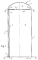
- FIG. 1 discloses a thermal process chamber 10 constructed according to the principles of the present invention.
- the thermal process chamber 10 is comprised of (i) a bell jar 11, which itself is comprised of a cylindrical main portion 12 and a closed end portion or domed crown 14; (ii) a base or lower flange 16; (iii) an injector tube 18 residing within the cylindrical main portion 12 of the bell jar 11; and (iv) a disc-shaped gas distribution plate 20, positioned within the bell jar 11 proximate at the junction of the cylindrical main portion 12 and the domed crown 14.
- the injector tube 18 and the distribution plate 20 function, as further described below, to evenly distribute process gas to the cylindrical main portion 12 of the bell jar 11.
- silicon carbide (SiC) is used to construct the cylindrical main portion 12 and the domed crown 14 of the bell jar 11, the lower flange 16, the injector tube 18, and the gas distribution plate 20.
- the entire process chamber 10 is assembled from these components in a "green” state, and then cured or hot-fired in an oven to complete an entire integral assembly.
- the cylindrical main portion 12 and the domed crown 14 of the bell jar 11 are formed of silicon carbide approximately 6 millimeters (mm) thick.
- Formed near the junction of the cylindrical main portion 12 and the domed crown 14 is an inwardly protruding ridge 22 that extends about the periphery of the bell jar 11.
- the ridge may be formed separately or may be formed integrally with either the cylindrical main portion 12 or the domed crown 14.
- the cylindrical main portion 12, the domed crown 14 and the inwardly extending ridge are joined together in their green state to form an uncured green bell jar 11.
- Figures 2 through 4 show, respectively, more detailed views of the remaining components of the process chamber 10, namely, the lower flange 16, the injector tube 18, and the gas distribution plate 20.
- the lower flange is constructed of an annular mass of silicon carbide.
- the thickness of the lower flange is on the order of 15 mm.
- the lower flange 16 is provided with an inwardly projecting protrusion 23, which provides means for mounting the lower end 24 of the injector tube 18 (see Figure 3) to the lower flange.
- the mounting means comprises a hole 26 in the protrusion 23, through which the lower end 24 of the injector tube 18 is inserted prior to curing .
- the hole 26 is provided with a ledge 28 which mates with a flange 30 to secure the position of the lower end 24 of the injector tube 18 in the flange protrusion 23.
- the upper end 32 of the injector tube 18 fits within a hole 34 (refer back to Figure 1) in the inwardly protruding ridge 22 of the bell jar 11.
- a hole 34 (refer back to Figure 1) in the inwardly protruding ridge 22 of the bell jar 11.
- the gas distribution plate 20 is positioned within the bell jar 11 by means of the inwardly protruding ridge 22.
- the inwardly-most protruding edge 36 of the ridge 22 extends inwardly beyond the outer perimeter 38 of the plate 20 to provide support for the plate.
- the entire process chamber assembly 10 is then hot-fired in an oven to fuse the components together.
- Vaporized silicon carbide is then applied to junctions formed by the joined components in a chemical vapor deposition (CVD) process.
- CVD chemical vapor deposition
- the deposition of such "filler material” insures that the process chamber 10 provides an air-tight, sealed environment for substrate processing.
- a gas such as nitrogen or oxygen is passed through the injector 18 into the interior 39 of the domed crown 14 of the bell jar 11.
- the gas flows from the domed crown downward, through passageways (channels or holes) 40, 42 in the gas distribution plate 20, and into the interior 44 of the main cylindrical portion 12 of the bell jar.
- Holes 40 near the center of the gas distribution plate 20 are spaced further apart from each other than those holes 42 about the periphery of the gas distribution plate. The closer spacing between the peripheral holes 42 is designed to alleviate pressure buildup that would tend to accumulate around the periphery of the interior of the domed crown 14.
- the sum total of the cross sectional area of the holes 40, 42 is approximately four times the cross sectional area of the injector tube 18 to eliminate any pressure buildup in the domed crown 14 of the bell jar 11.
- the pattern of holes 40, 42 disclosed provides an even flow of gas through the gas distribution plate. Accordingly, a substrate such as a silicon wafer (not shown) to be processed, positioned within the bell jar below and parallel to the gas distribution plate, will experience an even gas flow across the surface thereof.
- the gas is used primarily for oxide formation (e.g. , monitor oxides, gate oxides and mask oxides).
- oxide formation e.g. , monitor oxides, gate oxides and mask oxides.
- the silicon carbide construction can safely handle temperatures up to about 1250 degrees Centigrade (oC).
- silicon carbide is inert to processes occurring within the process chamber, unlike more active materials such as aluminum.
Abstract
Description
Claims (10)
- A thermal process chamber (10) for processing substrates contained therein, comprising:a main processing portion (12) in which a substrate to be processed may be positioned, said processing portion defining a first area (44) and providing an opening (21) through which a substrate to be processed may be inserted into and removed from said first area (44) of the process chamber;an upper portion (11), positioned above the main processing portion, defining a second area (39) and providing a closed end for the process chamber;a gas injector (18) for providing gas to said second area (39); anda gas distribution plate (20) separating said first area (44) from said second area (39), said gas distribution plate providing a plurality of passageways (40, 42) for permitting gas provided to said second area to pass into said first area, said gas distribution plate (20) formed integrally with said main processing portion (12) and with said upper portion (11).
- The thermal process chamber (10) of claim 1, wherein said main processing portion (12), said upper portion (11), said gas injector (18), and said gas distribution plate (20) are comprised of silicon carbide (SiC).
- The thermal process chamber (10) of claim 2, wherein said gas injector (18) comprises a tube extending from said opening (21) of said processing portion into said second area (39) of the process chamber.
- The thermal process chamber (10) of claim 3, further comprising a lower flange (16) defining said opening (21), said lower flange provided with a hole (26) into which a lower end (24) of said tube (18) is seated.
- The thermal process chamber (10) of claim 4, wherein said lower flange (16) is comprised of silicon carbide (SiC).
- The thermal process chamber (10) of claim 2, wherein said passageways (40, 42) in said gas distribution plate (20) comprise first passageways (40) and second passageways (42), said second passageways (42) positioned closer in proximity to each other than said first passageways (40).
- The thermal process chamber (10) of claim 6, wherein said second passageways (42) are positioned about the periphery (38) of said gas distribution plate (20).
- The thermal process chamber (10) of claim 4, further comprising an inwardly protruding ridge (22) extending about the inner periphery of the thermal process chamber, said ridge (22) providing an edge (36) against which said gas distribution plate (20) abuts for positioning said plate within the thermal process chamber.
- The thermal process chamber (10) of claim 8, wherein said ridge (22) is provided with a hole (34) at least partially through which an upper end (32) of said tube (18) passes.
- The thermal process chamber (10) of claim 2, further comprising vaporized silicon carbide applied via a chemical vapor deposition (CVD) process to junctions formed by said main processing portion (12), said upper portion (11), said gas injector (18), and said gas distribution plate (20).
Applications Claiming Priority (2)
| Application Number | Priority Date | Filing Date | Title |
|---|---|---|---|
| US468238 | 1999-12-21 | ||
| US09/468,238 US6302963B1 (en) | 1999-12-21 | 1999-12-21 | Bell jar having integral gas distribution channeling |
Publications (2)
| Publication Number | Publication Date |
|---|---|
| EP1111660A2 true EP1111660A2 (en) | 2001-06-27 |
| EP1111660A3 EP1111660A3 (en) | 2003-12-10 |
Family
ID=23858991
Family Applications (1)
| Application Number | Title | Priority Date | Filing Date |
|---|---|---|---|
| EP00311255A Withdrawn EP1111660A3 (en) | 1999-12-21 | 2000-12-15 | Bell jar having integral gas distribution channeling |
Country Status (5)
| Country | Link |
|---|---|
| US (1) | US6302963B1 (en) |
| EP (1) | EP1111660A3 (en) |
| JP (1) | JP4665204B2 (en) |
| KR (1) | KR100559198B1 (en) |
| TW (1) | TW499698B (en) |
Families Citing this family (5)
| Publication number | Priority date | Publication date | Assignee | Title |
|---|---|---|---|---|
| JP3472482B2 (en) * | 1998-06-30 | 2003-12-02 | 富士通株式会社 | Semiconductor device manufacturing method and manufacturing apparatus |
| KR100360401B1 (en) * | 2000-03-17 | 2002-11-13 | 삼성전자 주식회사 | Process tube having a slit type process gas injection portion and a waste gas exhaust portion of multi hole type and apparatus for semiconductor fabricating |
| US6576981B1 (en) * | 2001-07-03 | 2003-06-10 | Lsi Logic Corporation | Reduced particulate etching |
| FR3057390B1 (en) * | 2016-10-11 | 2018-12-07 | Soitec | VERTICAL OVEN WITH CONTAMINANT TRAPPING DEVICE |
| US11266005B2 (en) * | 2019-02-07 | 2022-03-01 | Fermi Research Alliance, Llc | Methods for treating superconducting cavities |
Family Cites Families (23)
| Publication number | Priority date | Publication date | Assignee | Title |
|---|---|---|---|---|
| JPS6226820A (en) * | 1985-07-26 | 1987-02-04 | Ibiden Co Ltd | Silicon carbide plasma dispersing plate |
| US5062386A (en) | 1987-07-27 | 1991-11-05 | Epitaxy Systems, Inc. | Induction heated pancake epitaxial reactor |
| JPH0642474B2 (en) | 1988-03-31 | 1994-06-01 | 株式会社東芝 | Semiconductor manufacturing equipment |
| JPH07120634B2 (en) * | 1988-12-27 | 1995-12-20 | 東京エレクトロン東北株式会社 | Processor |
| US5160545A (en) | 1989-02-03 | 1992-11-03 | Applied Materials, Inc. | Method and apparatus for epitaxial deposition |
| JP2729238B2 (en) * | 1989-12-22 | 1998-03-18 | 東京エレクトロン株式会社 | Vertical processing equipment |
| JP2992576B2 (en) * | 1990-03-31 | 1999-12-20 | 東京エレクトロン株式会社 | Vertical heat treatment equipment |
| JPH0468522A (en) * | 1990-07-10 | 1992-03-04 | Tokyo Electron Sagami Ltd | Vertical heat treatment device |
| JP3077195B2 (en) * | 1990-11-27 | 2000-08-14 | 日本電気株式会社 | Structure of vertical process tube for semiconductor heat treatment |
| JPH04196522A (en) * | 1990-11-28 | 1992-07-16 | Nec Corp | Vertical diffusion furnace |
| US5318633A (en) * | 1991-03-07 | 1994-06-07 | Tokyo Electron Sagami Limited | Heat treating apparatus |
| JPH04280420A (en) * | 1991-03-07 | 1992-10-06 | Toshiba Corp | Heat treatment device |
| JPH05251372A (en) * | 1992-03-06 | 1993-09-28 | Matsushita Electron Corp | Vertical type diffusion furnace |
| JPH0620980A (en) * | 1992-07-01 | 1994-01-28 | Nec Corp | Vertical heat treatment furnace |
| JP2805589B2 (en) * | 1994-01-27 | 1998-09-30 | 黄 哲周 | Low pressure chemical vapor deposition equipment |
| JPH08107082A (en) * | 1994-10-04 | 1996-04-23 | Sony Corp | Vertical heat treatment equipment |
| US5928427A (en) * | 1994-12-16 | 1999-07-27 | Hwang; Chul-Ju | Apparatus for low pressure chemical vapor deposition |
| US5653806A (en) | 1995-03-10 | 1997-08-05 | Advanced Technology Materials, Inc. | Showerhead-type discharge assembly for delivery of source reagent vapor to a substrate, and CVD process utilizing same |
| JPH09249455A (en) * | 1996-03-14 | 1997-09-22 | Toyo Tanso Kk | Production of silicon carbide compact |
| US6159297A (en) * | 1996-04-25 | 2000-12-12 | Applied Materials, Inc. | Semiconductor process chamber and processing method |
| KR100227850B1 (en) * | 1996-05-06 | 1999-11-01 | 윤종용 | Vertical diffusion furnace for both oxide film growth process and LP CVD process |
| US5976261A (en) | 1996-07-11 | 1999-11-02 | Cvc Products, Inc. | Multi-zone gas injection apparatus and method for microelectronics manufacturing equipment |
| US5653808A (en) * | 1996-08-07 | 1997-08-05 | Macleish; Joseph H. | Gas injection system for CVD reactors |
-
1999
- 1999-12-21 US US09/468,238 patent/US6302963B1/en not_active Expired - Fee Related
-
2000
- 2000-12-15 EP EP00311255A patent/EP1111660A3/en not_active Withdrawn
- 2000-12-15 KR KR1020000076881A patent/KR100559198B1/en not_active Expired - Fee Related
- 2000-12-19 TW TW089127172A patent/TW499698B/en not_active IP Right Cessation
- 2000-12-21 JP JP2000388743A patent/JP4665204B2/en not_active Expired - Fee Related
Also Published As
| Publication number | Publication date |
|---|---|
| TW499698B (en) | 2002-08-21 |
| US6302963B1 (en) | 2001-10-16 |
| JP2001237239A (en) | 2001-08-31 |
| EP1111660A3 (en) | 2003-12-10 |
| KR20010062458A (en) | 2001-07-07 |
| US20010037767A1 (en) | 2001-11-08 |
| JP4665204B2 (en) | 2011-04-06 |
| KR100559198B1 (en) | 2006-03-10 |
Similar Documents
| Publication | Publication Date | Title |
|---|---|---|
| US5855687A (en) | Substrate support shield in wafer processing reactors | |
| US7311784B2 (en) | Plasma processing device | |
| US5895530A (en) | Method and apparatus for directing fluid through a semiconductor processing chamber | |
| US6375748B1 (en) | Method and apparatus for preventing edge deposition | |
| KR100574116B1 (en) | Single wafer processing apparatus of semiconductor processing system | |
| JP4563984B2 (en) | Processing apparatus and processing method for reducing deposition on back surface of substrate | |
| US6444040B1 (en) | Gas distribution plate | |
| KR100770461B1 (en) | Gas treating device and film forming device | |
| JP2002513091A (en) | Improved heater for substrate processing equipment for depositing tungsten | |
| US6582522B2 (en) | Emissivity-change-free pumping plate kit in a single wafer chamber | |
| US10629427B2 (en) | Bevel etch profile control | |
| KR101014916B1 (en) | Emissivity Constant Pumping Plate Kit in Single Wafer Chamber | |
| US11948790B2 (en) | Heater support kit for bevel etch chamber | |
| US20220262657A1 (en) | Pedestal with multi-zone heating | |
| KR20030097861A (en) | Assembly comprising heat distributing plate and edge support | |
| US6302963B1 (en) | Bell jar having integral gas distribution channeling | |
| KR102689924B1 (en) | Heater support kit for sloped etch chambers | |
| KR20210076979A (en) | Shielding plate for CVD reactor | |
| KR20250038725A (en) | Purge ring for reduced substrate backside deposition | |
| JP2001257167A (en) | Semiconductor manufacturing equipment | |
| JP2002141290A (en) | Semiconductor manufacturing equipment | |
| CN121942343A (en) | Base heater | |
| US20220064785A1 (en) | Apparatus and methods for gas phase particle reduction | |
| TW202529167A (en) | Two-piece rf shield design | |
| KR100832713B1 (en) | Pedestal protectors for vertical furnaces |
Legal Events
| Date | Code | Title | Description |
|---|---|---|---|
| PUAI | Public reference made under article 153(3) epc to a published international application that has entered the european phase |
Free format text: ORIGINAL CODE: 0009012 |
|
| AK | Designated contracting states |
Kind code of ref document: A2 Designated state(s): AT BE CH CY DE DK ES FI FR GB GR IE IT LI LU MC NL PT SE TR |
|
| AX | Request for extension of the european patent |
Free format text: AL;LT;LV;MK;RO;SI |
|
| PUAL | Search report despatched |
Free format text: ORIGINAL CODE: 0009013 |
|
| AK | Designated contracting states |
Kind code of ref document: A3 Designated state(s): AT BE CH CY DE DK ES FI FR GB GR IE IT LI LU MC NL PT SE TR |
|
| AX | Request for extension of the european patent |
Extension state: AL LT LV MK RO SI |
|
| 17P | Request for examination filed |
Effective date: 20040602 |
|
| AKX | Designation fees paid |
Designated state(s): DE FR GB IT NL |
|
| 17Q | First examination report despatched |
Effective date: 20090218 |
|
| STAA | Information on the status of an ep patent application or granted ep patent |
Free format text: STATUS: THE APPLICATION IS DEEMED TO BE WITHDRAWN |
|
| 18D | Application deemed to be withdrawn |
Effective date: 20090630 |