EP1110078B1 - Adaptive lighting system and method for machine vision apparatus - Google Patents
Adaptive lighting system and method for machine vision apparatus Download PDFInfo
- Publication number
- EP1110078B1 EP1110078B1 EP99945459A EP99945459A EP1110078B1 EP 1110078 B1 EP1110078 B1 EP 1110078B1 EP 99945459 A EP99945459 A EP 99945459A EP 99945459 A EP99945459 A EP 99945459A EP 1110078 B1 EP1110078 B1 EP 1110078B1
- Authority
- EP
- European Patent Office
- Prior art keywords
- array
- lighting
- intensity
- light
- article
- Prior art date
- Legal status (The legal status is an assumption and is not a legal conclusion. Google has not performed a legal analysis and makes no representation as to the accuracy of the status listed.)
- Revoked
Links
Images








Classifications
-
- G—PHYSICS
- G01—MEASURING; TESTING
- G01N—INVESTIGATING OR ANALYSING MATERIALS BY DETERMINING THEIR CHEMICAL OR PHYSICAL PROPERTIES
- G01N21/00—Investigating or analysing materials by the use of optical means, i.e. using sub-millimetre waves, infrared, visible or ultraviolet light
- G01N21/84—Systems specially adapted for particular applications
- G01N21/88—Investigating the presence of flaws or contamination
- G01N21/8806—Specially adapted optical and illumination features
Definitions
- the present invention pertains to a lighting system for use with a machine vision apparatus, such as used in the inspection of semiconductor packages, wherein the lighting system automatically adapts to the particular object being inspected to provide an improved image of the object viewed by the vision apparatus to improve the accuracy of an inspection process or to carry out other processes.
- a lighting system which is set up for the proper contrast or image for one type of package usually requires adjustment for a different type of package.
- packages of essentially the same type or configuration may be fabricated of different materials which have at least slightly different light reflectivity characteristics. Therefore, a vision apparatus adapted for inspecting a particular type of semiconductor package may not function properly if slight changes in materials used for the packages or any changes in the light reflectivity of the package occurs which will change the contrast and the quality of the image captured by the inspection or vision apparatus.
- a lighting system for machine vision apparatus which is adaptable to vary the light intensity on various parts of an article or device being inspected, such as various types of integrated circuit or semiconductor packages, to enhance the image of the package, as viewed by a vision apparatus.
- a system which will automatically adjust the lighting imposed on different types of articles being inspected or otherwise viewed by a vision apparatus to enhance the accuracy of an inspection process or any process which requires machine vision of an article, such as an electronic circuit or semiconductor package.
- the intensity and pattern of the lighting imposed on different articles being inspected is important, it is also important to provide for monitoring the failure of any part of the lighting system so that improper lighting and inspection of articles being illuminated by the system is not experienced. It is to accomplish the desiderata mentioned above and overcome problems associated with prior art apparatus that the present invention has been developed.
- the present invention provides an improved lighting system for use with machine vision apparatus for inspecting or otherwise processing various types of articles including, in particular, electronic semiconductor devices or packages and the like.
- a lighting system which is adapted to provide a predetermined contrast or image quality of an article being viewed by a machine vision apparatus so that an accurate image of the article being viewed is produced.
- One embodiment of the adaptive lighting system is preferably provided with an array of light emitting diodes (LEDs), which are arranged in multiple geometric segments so that a plurality of LEDs in one segment of the array may emit light of a certain intensity while the light emitting elements (LEDs) of other segments are adjusted to emit light of other intensities to optimize the image of an article being inspected, which image may be captured by a machine vision apparatus.
- LEDs light emitting diodes
- an adaptive lighting system which includes a programmable lighting array intensity control circuit which is operable to control a substantial number of segments of an LED lighting array, in particular.
- the control circuit is operable in conjunction with a microprocessor which is operated with a program which performs lighting segment selection, intensity control for each segment energized and image intensity feedback.
- the programmable intensity control circuit includes a plurality of digitally controlled potentiometers, all arranged on a monolithic CMOS microcircuit.
- the complete intensity control circuit when interfaced with a digital input/output circuit connected to a microprocessor, will allow a vision apparatus to provide automatic adjustment of the light intensity on an article being illuminated and the provision of a substantial number of light intensity settings.
- the circuit is also adapted to include a constant current source for each lighting array segment and a single driver for both strobe and non-strobe illumination operations.
- An adaptive lighting system which includes a circuit for real time monitoring of light failure and providing a signal indicating at least one of the light segments of the lighting system has experienced a failure.
- the light failure monitoring circuit is included in a module provided for monitoring a failure of any of the lighting segments of the array or system and which includes an LED indicator for each light segment to indicate which segment has experienced a failure.
- the light failure monitoring circuit detects a discontinuity in or an open lighting circuit, reverse connections and LED failures resulting in either an open circuit or a short circuit.
- a lighting system is provided for use with machine vision apparatus which utilizes flash lamps and an array of fiber optic elements forming multiple light segments which may be used in place of or in addition to LED type lighting arrays to further increase the intensity of lighting for use in applications wherein the imaging system is required to capture an image of a moving object at very high "shutter" speeds.
- a lighting array including multiple bundles of fiber optic elements is coupled with an array of high intensity flash lamps providing the light source.
- a flash lamp driver/trigger circuit is operably coupled to the programmable light intensity controllers through DC to AC inverters. The flash lamps may be energized by a continuous high frequency signal or by a single pulse type signal to provide multiple modes of operation.
- the invention also provides a method for adjusting the intensity of a lighting array for lighting semiconductor packages and the like, which may be carried out by computing the median gray value of an image of an article or object, readjusting the lighting intensity and recomputing the median gray value until an optimum setting is reached.
- the adaptive lighting system of the present invention eliminates the need for microprocessor based digital to analog converter circuits of types commercially available at the time of development of the invention and which types have been sufficient to provide for only a very limited number of segments of a lighting array to be controlled.
- FIGURE 1 there is illustrated a generalized schematic diagram of a portion of a machine vision apparatus 18, including an adaptive lighting system 20, in accordance with the present invention.
- the lighting system 20 is adapted to be used in conjunction with machine vision apparatus 18, which may be one of the general types described in U.S. Patent Applications Serial Nos. 08/890,814 and 09/069,056 filed on July 11, 1997 and April 28, 1998, respectively, and assigned to the assignee of the present invention.
- the adaptive lighting system 20 is not limited to use with the apparatus disclosed in the above-identified patent applications and the lighting system may be operated to illuminate various devices.
- the system 20 is particularly adapted for illuminating electronic circuit or semiconductor devices or "packages", such as the package 22 shown in FIGURE 1 .
- the package 22 may be one of many types known to those skilled in the art of machine vision apparatus used in semiconductor device manufacturing.
- the package 22 may be disposed on a table, a transport belt or in a tray or other mechanism, all not shown, for moving the package 22 relative to the lighting system 20 into range to be illuminated by a lighting array 24.
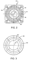
- the lighting array 24 includes a suitable support housing 26 in the form of a generally rectangular boxlike shell, having a top wall 28 with a central, generally cylindrical aperture 30 formed therein, for viewing the package 22 by a suitable camera 32.
- the camera 32 may be of a type commonly used in machine vision systems including a charge coupled device (CCD) type camera.
- CCD charge coupled device
- the lighting array 24 includes a suitable, somewhat dome-shaped annular support member 34 disposed within the housing 26 and operable to support three circular arrays 36, 38 and 40 of light emitting elements, preferably light emitting diodes (LEDs) 41, which are arranged concentrically about a central axis 42, which is also the central axis of the aperture 30.
- the three arrays 36, 38 and 40 of LEDs may each be subdivided into plural segments of one or more LEDs 41, as indicated by the diagram of FIGURE 3 .
- the inner ring array 40 is divided, by way of example, into segments 1 through 4, the intermediate ring array 38 is divided into segments 5 through 8 and the outer ring array 36 of LEDs is divided into segments 9 through 12, as indicated.
- each of the segments which comprises one fourth of a circular arc, may be further subdivided into additional segments, if desired.
- the housing 26 has a substantially open bottom side to allow light emitted by the arrays 36, 38 and 40 of LEDs 41 to project onto the package 22 or any article which is placed under the dome-shaped support structure 34 for the LED arrays.
- the LED lighting array 24 may be suitably mounted on a machine vision apparatus together with the camera 32 so that a transport path for circuit packages 22 will place each package in the position shown in FIGURE 1 to be fully illuminated by the array 24.
- the lighting array 46 includes a generally rectangular box shaped housing 48, having a top wall 50 in which a central rectangular aperture 52 is formed.
- the bottom side of the housing 48 is essentially open like the housing 26.
- a support structure 54 is disposed in the housing 50 and supports four circumferentially spaced linear arrays of LEDs indicated by numerals 56, 58, 60 and 62 and an inner rectangular ring array 64 around the aperture 52.
- Each of the LED arrays 56, 58, 60 and 62 includes three rows of LEDs 63, as shown.
- the LED array 46 may be used in place of the LED array 24, if desired.
- the lighting system 20 is adapted to be operated by a digital computer or central processing unit 66, which includes a plurality of components, including a so-called frame grabber circuit 68, a programmable processor 70, a memory circuit 72 and a programmable light intensity control circuit 74.
- the light intensity control circuit 74 interfaces with a suitable input/output circuit or card 76 interconnected with the processor 70 and the programmable light intensity control circuit 74 for operation of same to vary the light intensity of the segments of the LED arrays 36, 38 and 40 to provide a suitable illumination and contrast between the package 22 so that the camera 32 may capture a high resolution image of the package 22 for various purposes known to those who are skilled in the art.
- FIGURE 1 Semiconductor packages operable to be inspected by a vision apparatus including the lighting system 20 are usually provided with a preselected indicia on the surface 22a, FIGURE 1 .
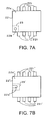
- a representative example of surface indicia is shown on surface 22a of a semiconductor package 22 comprising a small dimple or depression 22b in the surface 22a in the lower left corner, as indicated.
- FIGURE 7B Another example is shown in FIGURE 7B wherein a semiconductor package 22' has a surface 22a' on which a notch-shaped depression 22b' is formed midway between opposite sides of the package body.
- the camera 32 obtains an image within a defined window 23 or 23', see FIGURES 7A and 7B , which is recorded by processor unit 66 and memory 72 is queried to identify the type of package being inspected.
- the light intensity adjustment is then carried out for capturing a desired image of the package 22 or 22' for inspection purposes or the like based on measurement taken from windows 23 or 23' or from the entire package including sets of leads 221 or 221'.
- FIGURE 8 there is illustrated a flow chart indicating the basic steps that the processor 66 takes to adjust the light intensity emitted by the array 24.
- the steps indicated in FIGURE 8 include a histogram process which is described further herein.
- the processor 66 is programmed to calculate a histogram or a pixel intensity distribution of a specified source buffer and store the result in a specified histogram result buffer.
- the source buffer is derived from the defined windows 23 or 23' on a captured image of a package.
- the median gray value of the camera pixel intensity distribution for camera 32 is less than a predetermined threshold value for a particular type of semiconductor package being viewed, and a predefined set of light segments is not already energized to full intensity the light intensity emitted by the selected segments is then increased a predetermined incremental amount and another image is captured. This process is repeated until the median gray value of the pixel intensity distribution is substantially equal to the predetermined threshold value. In this instance, the final intensity level of the selected light segments is saved to a configuration file for future use in inspecting packages of the same type.
- the basic steps in the process of capturing a well defined image of a package 22 or 22' comprise preconditioning the processor 66, when a known type of package is to be inspected, to retrieve a threshold value of image intensity and selected lighting array segments to be used for illuminating the package from a configuration file stored in the processor memory 72, as indicated by step 80 in FIGURE 8 .
- the processor 66 may be operated to retrieve the image intensity threshold value and selected lighting segments information upon the camera 32 and processor 66 recognizing the package type from obtaining an image of the package identifier indicia 22b or 22b', for example.
- the lighting system 20 may be operated in accordance with the method of the invention wherein the start of the operation is initiated by a package 22 presenting itself in viewing range of camera 32 to cause the camera and processor unit 66 to provide a trigger signal from frame grabber 68 to control circuit 74.
- a trigger signal to initiate operation of control circuit 74 may be responsive to a sensor, not shown, associated with vision apparatus 18 which senses when the known type of package has been positioned for capturing an image with camera 32.
- an image of a package to be inspected is captured by the camera 32 with the lighting array 24 illuminating the package in accordance with preselected lighting array segments operating at preselected light emitting intensities.
- the image capture step is indicated at step 82 in FIGURE 8 .
- the histogram process includes the provision of a histogram of the intensity distribution of the camera pixel values for the camera 32 of an image of a particular semiconductor package.
- the median gray value of the accumulated histogram is selected as the threshold level of the image intensity distribution.
- an adaptive lighting system such as the system 20
- the threshold value or the median value of the pixel intensity distribution is retrieved from a configuration file and compared with a median value of pixel intensity distribution at a minimum intensity setting of the lighting array 24 using the predetermined lighting segments for inspecting the semiconductor package in question.
- This threshold value for good image contrast is retrieved from the configuration file and compared with the median value at the minimum light intensity setting and, if the median value is greater than the threshold value, the light intensity level is increased and a new image is captured of the semiconductor package of the type in question.
- the median value of the accumulated histogram including the newly processed image is computed and compared again with the threshold value. This process is repeated at different incrementally increasing light intensity levels for the lighting segments selected until the median value reaches, approximately, the threshold value.
- the final light intensity setting at this condition of median value versus threshold value is saved to the aforementioned configuration file in the memory 42, for example, for the particular package type. This setting then is used in the next lot of packages of a similar type to be inspected by an inspection system, for example, using the machine vision apparatus 18, for example.
- a verification process is performed to determine if the median value of the image remains close to the threshold value so that the inspection process can be carried out. During the verification process, however, if the median value is far from the threshold value, the process just described is performed again starting from the minimum intensity level of the lighting array segments being energized until the above-mentioned optimum setting is reached. The verification process is considered necessary in order to adapt the lighting array to properly illuminate the surface of the package in question.
- step 86 when the median gray value determined by the histogram process exceeds the threshold value obtained from step 80, at step 86, and all selected lighting segments are energized at maximum intensity an error message is indicated to the system operator in accordance with step 88. If all selected lighting segments are not at maximum intensity, as indicated from the configuration file, then the intensity of each of the operating lighting segments is increased by one "step" or increment, as indicated at step 90, and another image is captured, and the histogram process carried out. Once the median gray value obtained in the histogram process is substantially equal to the threshold value the final intensity level of the selected lighting segments is saved to the configuration file for the next inspection process for the same type of package as described, and as indicated in step 92.
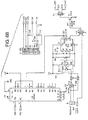
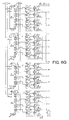
- FIGURES 6A through 6G there is illustrated a schematic diagram of the programmable intensity control circuit 74 for controlling the intensity of various segments of the lighting array described above and shown in FIGURES 2 and 3 .
- the particular control circuit 74 shown in drawing FIGURES 6A through 6G is designed to provide selection of multiple LED segments up to a maximum of sixty-four segments and each segment can have its light output intensity programmed for operation at up to sixty-four incremental intensity levels.
- each LED segment is driven by a constant current source which provides an option for strobe or non-strobe operation of the lighting array 24.
- the circuit 74 is capable of high speed switching within a switching time of about 200 nanoseconds between respective sets of LED segments which have been preprogrammed to operate at the switched intensity levels.
- the lighting array 24 may provide for rapidly capturing two images of a package 22 by the camera 32 at different lighting intensity settings of the array 24.
- control circuit 74 is adapted to be coupled externally with I/O card 76 which is inserted in a suitable card slot in a conventional central processing unit such as an IBM PC-AT digital computer, for example.
- the control circuit 74 includes a decoding circuit, FIGURE 6A , including a decoder/multiplexer U41 which is operably connected to bi-stable latches, as shown and designated U42.
- decoding circuit FIGURE 6A
- U41 which is operably connected to bi-stable latches, as shown and designated U42.
- These circuit elements are connected between the input/output circuit 76 and non-volatile digital potentiometers indicated by the designators U17 through U33, see FIGURES 6B through 6G also.
- the potentiometers U17 through U33 may be of a type available from Xicor, Inc., Milpitas, CA, as their Part No. X9241WP.
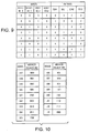
- the control bits used and the logic of the serial outputs to the digital potentiometers are shown in FIGURE 9 .
- signal paths SCL1 and SCL2, FIGURE 6A are clock inputs to the potentiometers U17 through U33 to clock data into and out of these circuits.
- Signal paths SDA1 and SDA2 are bi-directional and are used to transfer data into and out of the potentiometers U17 through U33.
- Signal paths SCL1, SCL2, SDA1 and SDA2 and power paths VH, VL and VD, VS carry numerical correlation prefixes between FIGURES 6C and 6G for convenience.
- Potentiometers U17 through U32 are assigned unique addresses through terminals A0, A1, A2, A3, respectively. The address assignments are indicated in FIGURE 10 .
- Potentiometers U17 through U32 are connected to provide, by way of example, sixty-four resistor arrays each composed of sixty-four wiper elements.
- the position of a wiper element for an array is controlled by the user through signal paths SDA1 and SCL1.
- Control of a wiper element through the two wire serial interface may be carried out using published data available from Xicor, Inc. for the X9241WP non-volatile digital potentiometer.
- circuit U33 For operation of the lighting array 24 in a strobe mode, circuit U33, FIGURE 6B , provides for two resister arrays cascaded to provide a variable resistance to a timing circuit for a monostable multi-vibrator U36.
- the position of the wiper element on each array segment is controlled by the user through signal conductors SDA2 and SCL2.
- the timing circuit for multivibrator U36 is determined by the cascaded resistances and capacitance C28 to provide a desired output signal pulse duration at output terminal Q of the multivibrator. This pulse is obtained when terminal B is being edge triggered by an input trigger signal from processor 70 by way of trigger input terminal J5, hex inverter U34 and opto-isolator U35.
- FIGURE 6B During the "on" pulse duration, power transistor Q1, FIGURE 6B , is activated to energize all the LED segments of array 24 simultaneously.
- the strobe mode may be enabled through connector J2 and signal path LEDSTR, FIGURES 6A and 6B , from processor 70.
- FIGURE 6B also illustrates a schematic for a multi-terminal connector J1 which provides for the appropriate power paths of plus 24 volts, plus 12 volts, plus 5 volts and minus 5 volts from a suitable source, not shown.
- Capacitors C29, C30 and C31 are connected as shown to provide suitably stable voltages at the respective levels indicated.
- control circuit 74 provides for operation of high speed switching between two "banks" or sections of LED segments so that the light intensity pattern of illumination on a package 22, for example, may be rapidly switched from one to another to allow image capture of each pattern by the camera 32 for comparison purposes.
- the output signals from the potentiometers U17, U18, U19 and U20 are transmitted through respective SPDT CMOS analog switches U46, U47, U48 and U49.
- Switches U46, U47, U48 and U49 are also operably connected to the output pins indicated in the circuit diagrams of potentiometers U21, U22, U23 and U24, respectively.
- Switches U46, U47, U48 and U49 are actuated through a signal from processor 70 by way of a suitable signal path through connector J2 shown in FIGURE 6B to the jumper socket E4 shown in FIGURE 6C .
- Each of switches U46, U47, U48 and U49 is operable to receive a switching signal via the above-described path as indicated in FIGURES 6C and 6D .
- the settings of the potentiometers U17, U18, U19 and U20 may be imposed on either the lighting segments normally connected to these potentiometers or the lighting segments normally connected to the potentiometers U21, U22, U23 and U24 to provide two different lighting patterns for illuminating a package, such as the package 22.
- the lighting pattern switching speed may be about 200 nanoseconds using the components of the control circuit 74. In this way, the camera 32 may capture two images rapidly at two different light intensity settings and whereby the processor unit 66 may compare the images for identification and inspection purposes, for example.
- each LED segment is provided with a constant current source which consists of operational amplifiers U1A to U1D through U16A to U16D as shown in FIGURES 6C to 6G , which amplifiers are respectively coupled with power MOSFETS CR1 to CR64.
- the limiting current for each segment is set by a 100 ohm resistor, R1 through 64.
- the output signals from the control circuit 74 and power signals are imposed on the segments of LEDs 41 of the array 24 through multi-conductor connectors J3 and J4, see FIGURES 6C through 6G .
- FIGURES 11A and 11B these figures are intended to be read together when joined at line a-a.
- the components identified in FIGURES 11A and 11B which bear reference designations the same as shown for components in FIGURES 6A through 6G are differentiated by the sign.
- FIGURES 11A and 11B illustrate a diagram of a portion of a circuit for a light failure "module" for monitoring the failure of any of the LEDs of a segment of the LED array 24, for example.
- the circuit diagram of FIGURES 11A-11B illustrate the light failure module or circuitry for two LED arrays or segments. The circuitry may be repeated for the total number of segments present in an LED array such as the array 24.
- connector P2 receives a twenty-four volt DC power supply from the system 20 and steps this voltage to a five volt DC supply at regulator U9'.
- the circuit shown in FIGURE 11B includes a programmable logic device U10' which also operates on a five volt DC supply and is programmed to generate alarm signals at connector P3. Multiple voltage signals are input at connector P2 through, for example, conductors VS0, VS1, VS2, and VS3, which are, respectively, operably connected to pin 3 of MOSFETS CR1 through CR8, respectively, for example.
- a voltage signal to LED array 1 and LED D1 from voltage comparator U1A will signal a "failure" in the light segment associated with MOSFET CR1, FIGURE 6D , if there exists an open circuit condition or reversed connections to the LED light segment associated with MOSFET CR1.
- the input voltage signal from MOSFET CR1 to comparators U1A and U1B is compared to a reference voltage at potentiometers or trimmers TP1 and TP2. If the input voltage is greater than reference voltage VR1 or less than voltage VR2, see FIGURE 11A , the LED indicator D1 turns on indicating a light failure on the associated segment of the LED lighting array. Similar circuitry applies to each light segment.
- Input signals are also provided at connectors P5 from constant current voltage provided at pin 2 of MOSFETS CR1 through CR16, respectively. These constant current voltages are input to an adder circuit using an op amp U11A, as shown by way of example for the circuit associated with MOSFET CR1, FIGURE 11A . Each op amp circuit combines the light segment voltage with the constant current voltage. The resultant voltage is input to a comparator U15A, for example, to detect a failure of an LED in a segment of the lighting array 24 resulting in a short circuit. The resultant voltage is compared with a reference voltage at potentiometer or trimmer TP9, for example.
- the indicator D1 turns on also indicating a light failure in the associated LED lighting segment.
- this circuitry applies to each of the light segments of the LED lighting array 24 and may be repeated for up to the 64 segments referenced with regard to FIGURE 6C through 6G .
- the light failure module described and shown provide an important and advantageous feature for the adaptive lighting system 20.
- the lighting system 120 may utilize an enclosure or housing 122 for supporting an array of fiber optic elements 124, each having a light input head 126, as shown in FIGURE 12 , and one or more light output heads 128 arranged in particular patterns, as illustrated, within the enclosure or support 122.
- the entire lighting array of system 120 may be made up of the optical fiber elements 124 having light input heads 126 and one or more light output heads 128 arranged as illustrated.
- four arrays of ten light output heads 128 are arranged in a rectangular pattern together with four arrays of two light output heads 128 interposed the arrays of ten output heads, respectively.
- This lighting array may be used in place of the lighting array shown in FIGURES 4 and 5 , for example, and may be supplemented by additional arrays of four output heads 128 each disposed in a position beneath the semiconductor package to be inspected and suitably supported on a support member 122b, for example.
- the lighting array shown schematically in FIGURE 12 may be used alone or used to supplement the light output of an array of LED light sources.
- the opposed segments of ten light output heads 128 are indicated by numerals 130a, 130b, 130c and 130d and the intermediate arrays illustrated are indicated by numerals 131a, 131b, 131c and 131d.
- Other arrays or arrangements of the multiple light output heads 128 are possible.
- the opposed arrays which may be disposed below the package are indicated by numerals 132a, 132b, 132c and 132d.
- the optical fiber elements 124 are adapted to transmit light provided by multiple flash lamps 136 with at least one flash lamp arranged in proximity to a light input head 126 of an optical fiber element or bundle of elements 124. Sixteen flash lamps 136 are shown schematically in FIGURES 12 and 13 .
- the flash lamps 136 are arranged in groups of four each for the exemplary system 120 and are operably connected to switches U46, U47, U48 and U49 by way of respective DC to AC inverter circuits 140 and corresponding flash lamp driver and trigger circuits 142, as illustrated generally by the block diagram of FIGURE 13 . Accordingly, the output signals from switches U46, U47, U48 and U49 are input to the circuits of FIGURE 13 in place of the LED arrays connected to these switches as shown for the embodiment whose circuit is illustrated in FIGURES 6C and 6D .
- the flash lamps 136 are driven by the sixteen sets of flash lamp drivers and triggers which obtain variable DC output voltage signals from the potentiometers U17, U18, U19 and U20 by way of the switches U46, U47, U48 and U49 and by way of the DC to AC inverters 140.
- the flash lamps 136 may be provided as one of a type commercially available.
- a common input signal is provided to trigger all of the flash lamp driver and trigger circuits simultaneously.
- the DC to AC inverters 140 may also be one of a type commercially available.
- FIGURE 14 a more detailed schematic diagram is shown indicating how the flash lamp strobe signal may be generated.
- An external trigger signal may be generated by one of the light intensity programmable controllers U17, U18, U19, or U20 for each array segment which signal is transmitted through transistor Q1 in FIGURE 14 and is input to pin NO1 of one of the switches U46, U47, U48 or U49, as the case may be.
- a test enable signal may also be imposed on one of the switches U46, U47, U48 or U49 at pin IN1.
- a continuous strobe output signal which may be varied in frequency from zero to twenty-five Hz, is provided at output pin COM1 for the respective switch U46, U47, U48 or U49.
- a timer circuit comprising, for example, a circuit 144 in FIGURE 14 is connected to input terminal NC1 of the relevant switch U46, U47, U48 or U49. Accordingly, a single strobe output signal from switch U46, U47, U48 or U49 is provided when a test enable signal is inactive and an external trigger signal from a light intensity programmable controller is active.
- a test enable signal is input to one of the switches U46, U47, U48 or U49, a continuous strobe signal in a selected frequency range is provided at switch output pin COM1.
- the timers 144 are each controlled by an external resistor and capacitor circuit shown in FIGURE 14 .
- FIGURE 15 one of the flash lamp driver/trigger circuits 142 is illustrated.
- a variable voltage signal received from a DC to AC inverter 140 associated with a circuit 142 is connected to the primary side 146 of a center tapped transformer 147, as shown in FIGURE 15 .
- the winding ratio of transformer 147 is about 1:46.
- Variable secondary voltages charge storage capacitor 148 through the circuit, as shown in FIGURE 15 , to an RMS voltage of up to three hundred twenty five volts DC maximum. This voltage in turn charges trigger capacitor 150 through trigger resistor 152.
- a strobe signal of about one volt at twenty miliamps is present at the gate of triac 154 from the circuitry, shown in FIGURE 14 , for example, the trigger capacitor 150 will discharge through transformer 156 to energize flash lamp 136.
- a correlation table for certain ones of the circuit elements commercially available and not otherwise identified follows: Commercial Part No. Ref. No. Description Mfr. SN74LS155A U41 IC, DUAL 2-LINE TO 4 LINE DECODERS/ DEMULTIPLEXERS TI SN74LS375 U42 IC, 4-BIT BISTABLE LATCHES TI SN7404 U43,U44 IC, HEX INVERTERS TI SN74LS125A U45 IC, QUAD BUS BUFFERS WITH 3-STATE OUTPUTS TI TL084CN U1-U16 JFET INPUT OPERATION AMPLIFIERS TI X9241WP U17-U33 QUAD CMOS EEPOT, 10K OHMS XICOR SN74LS04 U34 IC, HEX INVERTERS TI 585-292 U35 IC, OPTO-ISOLATOR, SCHMITT TRIGGER HIU RS SN74121 U36 IC, MONOSTABLE
- a correlation table for certain ones of the circuit elements commercially available and not otherwise identified follows: Commercial Part No. Ref. No. Description Mfr. SN74LS155A U41 IC, DUAL 2-LINE TO 4 LINE DECODERS/ DEMULTIPLEXERS TI SN74LS375 U42 IC, 4-BIT BISTABLE LATCHES TI SN7404 U43,U44 IC, HEX INVERTERS TI SN74LS125A U45 IC, QUAD BUS BUFFERS WITH 3-STATE OUTPUTS TI TL084CN U1-U16 JFET INPUT OPERATION AMPLIFIERS TI X9241WP U17-U33 QUAD CMOS EEPOT, 10K OHMS XICOR SN74LS04 U34 IC, HEX INVERTERS TI 585-292 U35 IC, OPTO-ISOLATOR, SCHMITT TRIGGER HIU RS SN74121 U36 IC, MONOSTABLE
Landscapes
- Physics & Mathematics (AREA)
- Health & Medical Sciences (AREA)
- Life Sciences & Earth Sciences (AREA)
- Chemical & Material Sciences (AREA)
- Analytical Chemistry (AREA)
- Biochemistry (AREA)
- General Health & Medical Sciences (AREA)
- General Physics & Mathematics (AREA)
- Immunology (AREA)
- Pathology (AREA)
- Investigating Materials By The Use Of Optical Means Adapted For Particular Applications (AREA)
Abstract
Description
- The present invention pertains to a lighting system for use with a machine vision apparatus, such as used in the inspection of semiconductor packages, wherein the lighting system automatically adapts to the particular object being inspected to provide an improved image of the object viewed by the vision apparatus to improve the accuracy of an inspection process or to carry out other processes.
- In the manufacture of semiconductor or microelectronic circuits or so-called packages, several processes may be carried out by machine vision systems, including inspection of the package electrical leads to determine if any leads are out of place or damaged, or inspection of the package for certain markings placed thereon. Machine vision systems have been developed to carry out these tasks in view of the need to automate the manufacturing process for semiconductor packages, taking into consideration the substantial number of such packages which are produced. Moreover, many inspection and marking systems for processing semiconductor packages are adapted to handle various configurations of packages having different shapes, lead configurations and light reflecting characteristics. Such a vision system is disclosed for example in
US 4 882 498 . - In this last mentioned regard, a lighting system which is set up for the proper contrast or image for one type of package usually requires adjustment for a different type of package. Still further, packages of essentially the same type or configuration may be fabricated of different materials which have at least slightly different light reflectivity characteristics. Therefore, a vision apparatus adapted for inspecting a particular type of semiconductor package may not function properly if slight changes in materials used for the packages or any changes in the light reflectivity of the package occurs which will change the contrast and the quality of the image captured by the inspection or vision apparatus.
- Accordingly, there has been a need for a lighting system for machine vision apparatus which is adaptable to vary the light intensity on various parts of an article or device being inspected, such as various types of integrated circuit or semiconductor packages, to enhance the image of the package, as viewed by a vision apparatus. Moreover, there has also been a need for a system which will automatically adjust the lighting imposed on different types of articles being inspected or otherwise viewed by a vision apparatus to enhance the accuracy of an inspection process or any process which requires machine vision of an article, such as an electronic circuit or semiconductor package. Still further, since the intensity and pattern of the lighting imposed on different articles being inspected is important, it is also important to provide for monitoring the failure of any part of the lighting system so that improper lighting and inspection of articles being illuminated by the system is not experienced. It is to accomplish the desiderata mentioned above and overcome problems associated with prior art apparatus that the present invention has been developed.
- The present invention provides an improved lighting system for use with machine vision apparatus for inspecting or otherwise processing various types of articles including, in particular, electronic semiconductor devices or packages and the like.
- In accordance with one important aspect of the present invention a lighting system is provided which is adapted to provide a predetermined contrast or image quality of an article being viewed by a machine vision apparatus so that an accurate image of the article being viewed is produced. One embodiment of the adaptive lighting system is preferably provided with an array of light emitting diodes (LEDs), which are arranged in multiple geometric segments so that a plurality of LEDs in one segment of the array may emit light of a certain intensity while the light emitting elements (LEDs) of other segments are adjusted to emit light of other intensities to optimize the image of an article being inspected, which image may be captured by a machine vision apparatus.
- In accordance with the present invention, an adaptive lighting system is provided which includes a programmable lighting array intensity control circuit which is operable to control a substantial number of segments of an LED lighting array, in particular. Moreover, the control circuit is operable in conjunction with a microprocessor which is operated with a program which performs lighting segment selection, intensity control for each segment energized and image intensity feedback.
- In particular, the programmable intensity control circuit includes a plurality of digitally controlled potentiometers, all arranged on a monolithic CMOS microcircuit. The complete intensity control circuit, when interfaced with a digital input/output circuit connected to a microprocessor, will allow a vision apparatus to provide automatic adjustment of the light intensity on an article being illuminated and the provision of a substantial number of light intensity settings. The circuit is also adapted to include a constant current source for each lighting array segment and a single driver for both strobe and non-strobe illumination operations.
- An adaptive lighting system is provided which includes a circuit for real time monitoring of light failure and providing a signal indicating at least one of the light segments of the lighting system has experienced a failure. The light failure monitoring circuit is included in a module provided for monitoring a failure of any of the lighting segments of the array or system and which includes an LED indicator for each light segment to indicate which segment has experienced a failure. The light failure monitoring circuit detects a discontinuity in or an open lighting circuit, reverse connections and LED failures resulting in either an open circuit or a short circuit.
- A lighting system is provided for use with machine vision apparatus which utilizes flash lamps and an array of fiber optic elements forming multiple light segments which may be used in place of or in addition to LED type lighting arrays to further increase the intensity of lighting for use in applications wherein the imaging system is required to capture an image of a moving object at very high "shutter" speeds. A lighting array including multiple bundles of fiber optic elements is coupled with an array of high intensity flash lamps providing the light source. A flash lamp driver/trigger circuit is operably coupled to the programmable light intensity controllers through DC to AC inverters. The flash lamps may be energized by a continuous high frequency signal or by a single pulse type signal to provide multiple modes of operation.
- The invention also provides a method for adjusting the intensity of a lighting array for lighting semiconductor packages and the like, which may be carried out by computing the median gray value of an image of an article or object, readjusting the lighting intensity and recomputing the median gray value until an optimum setting is reached.
- The adaptive lighting system of the present invention eliminates the need for microprocessor based digital to analog converter circuits of types commercially available at the time of development of the invention and which types have been sufficient to provide for only a very limited number of segments of a lighting array to be controlled.
- Those skilled in the art will further appreciate the advantages and superior features of the invention together with other important aspects thereof on reading the detailed description which follows in conjunction with the drawing.
-
-
FIGURE 1 is a schematic diagram of a machine vision apparatus including an adaptive lighting system in accordance with the invention; -
FIGURE 2 is a plan view of a dome-shaped lighting array in accordance with one embodiment of the invention; -
FIGURE 3 is a diagram illustrating the number of segments of the lighting array shown inFIGURES 1 and2 which are independently controllable in accordance with one embodiment of the invention; -
FIGURE 4 is a plan view of an alternate embodiment of a lighting array in accordance with the invention; -
FIGURE 5 is a section view taken along the line 5-5 ofFIGURE 4 showing further details of the alternate lighting array; -
FIGURES 6A through 6G comprise a circuit diagram for a programmable light intensity control circuit in accordance with the invention; -
FIGURES 7A and 7B illustrate respective integrated circuit or semiconductor packages having package identifying indicia thereon; -
FIGURE 8 is a flow chart showing certain steps in a method of operation of the adaptive lighting system of the invention; -
FIGURE 9 is a logic table; -
FIGURE 10 is an address assignment table for components of the circuit shown inFIGURES 6A through 6G ; -
FIGURES 11A and11B comprise a circuit diagram of a portion of a light failure module for the lighting system of the invention; -
FIGURE 12 is a diagram of an alternate embodiment of a lighting array in accordance with the invention; -
FIGURE 13 is a block diagram of the major components of the lighting array of the embodiment shown inFIGURE 12 ; -
FIGURE 14 is a detail schematic diagram of the switching and timing circuit for generating a signal to energize one of the flash lamps; and -
FIGURE 15 is a detail schematic of a flash lamp driver and trigger circuit for the embodiment ofFIGURES 12 and13 . - In the description which follows like parts are marked throughout the specification and drawing with the same reference numerals, respectively. The drawing figures may not be to scale and certain components may be shown in generalized or schematic form and identified by commercial designations in the interest of clarity and conciseness.
- Referring to
FIGURE 1 , there is illustrated a generalized schematic diagram of a portion of amachine vision apparatus 18, including anadaptive lighting system 20, in accordance with the present invention. Thelighting system 20 is adapted to be used in conjunction withmachine vision apparatus 18, which may be one of the general types described inU.S. Patent Applications Serial Nos. 08/890,814 09/069,056 adaptive lighting system 20 is not limited to use with the apparatus disclosed in the above-identified patent applications and the lighting system may be operated to illuminate various devices. However, thesystem 20 is particularly adapted for illuminating electronic circuit or semiconductor devices or "packages", such as thepackage 22 shown inFIGURE 1 . Thepackage 22 may be one of many types known to those skilled in the art of machine vision apparatus used in semiconductor device manufacturing. - The
package 22 may be disposed on a table, a transport belt or in a tray or other mechanism, all not shown, for moving thepackage 22 relative to thelighting system 20 into range to be illuminated by alighting array 24. Thelighting array 24 includes asuitable support housing 26 in the form of a generally rectangular boxlike shell, having atop wall 28 with a central, generallycylindrical aperture 30 formed therein, for viewing thepackage 22 by asuitable camera 32. Thecamera 32 may be of a type commonly used in machine vision systems including a charge coupled device (CCD) type camera. - Referring also to
FIGURE 2 , thelighting array 24 includes a suitable, somewhat dome-shapedannular support member 34 disposed within thehousing 26 and operable to support threecircular arrays central axis 42, which is also the central axis of theaperture 30. The threearrays more LEDs 41, as indicated by the diagram ofFIGURE 3 . Theinner ring array 40 is divided, by way of example, intosegments 1 through 4, theintermediate ring array 38 is divided intosegments 5 through 8 and theouter ring array 36 of LEDs is divided intosegments 9 through 12, as indicated. Each of the segments, which comprises one fourth of a circular arc, may be further subdivided into additional segments, if desired. As shown inFIGURES 1 and2 , thehousing 26 has a substantially open bottom side to allow light emitted by thearrays LEDs 41 to project onto thepackage 22 or any article which is placed under the dome-shaped support structure 34 for the LED arrays. TheLED lighting array 24 may be suitably mounted on a machine vision apparatus together with thecamera 32 so that a transport path forcircuit packages 22 will place each package in the position shown inFIGURE 1 to be fully illuminated by thearray 24. - Referring briefly to
FIGURES 4 and 5 , an alternate embodiment of an LED lighting array for use in conjunction with theadaptive lighting system 20 is illustrated and generally designated by the numeral 46. Thelighting array 46 includes a generally rectangular box shapedhousing 48, having atop wall 50 in which a centralrectangular aperture 52 is formed. The bottom side of thehousing 48 is essentially open like thehousing 26. Asupport structure 54 is disposed in thehousing 50 and supports four circumferentially spaced linear arrays of LEDs indicated bynumerals rectangular ring array 64 around theaperture 52. Each of theLED arrays LEDs 63, as shown. TheLED array 46 may be used in place of theLED array 24, if desired. - Referring again to
FIGURE 1 , thelighting system 20 is adapted to be operated by a digital computer orcentral processing unit 66, which includes a plurality of components, including a so-calledframe grabber circuit 68, a programmable processor 70, amemory circuit 72 and a programmable lightintensity control circuit 74. The lightintensity control circuit 74 interfaces with a suitable input/output circuit orcard 76 interconnected with the processor 70 and the programmable lightintensity control circuit 74 for operation of same to vary the light intensity of the segments of theLED arrays package 22 so that thecamera 32 may capture a high resolution image of thepackage 22 for various purposes known to those who are skilled in the art. - Semiconductor packages operable to be inspected by a vision apparatus including the
lighting system 20 are usually provided with a preselected indicia on thesurface 22a,FIGURE 1 . For example, as shown inFIGURE 7A , a representative example of surface indicia is shown onsurface 22a of asemiconductor package 22 comprising a small dimple ordepression 22b in thesurface 22a in the lower left corner, as indicated. Another example is shown inFIGURE 7B wherein a semiconductor package 22' has asurface 22a' on which a notch-shapeddepression 22b' is formed midway between opposite sides of the package body. When apackage 22 or 22' is presented for inspection under thelighting array 24, thecamera 32 obtains an image within a definedwindow 23 or 23', seeFIGURES 7A and 7B , which is recorded byprocessor unit 66 andmemory 72 is queried to identify the type of package being inspected. The light intensity adjustment is then carried out for capturing a desired image of thepackage 22 or 22' for inspection purposes or the like based on measurement taken fromwindows 23 or 23' or from the entire package including sets ofleads 221 or 221'. - Referring briefly to
FIGURE 8 , there is illustrated a flow chart indicating the basic steps that theprocessor 66 takes to adjust the light intensity emitted by thearray 24. The steps indicated inFIGURE 8 include a histogram process which is described further herein. Basically, theprocessor 66 is programmed to calculate a histogram or a pixel intensity distribution of a specified source buffer and store the result in a specified histogram result buffer. The source buffer is derived from the definedwindows 23 or 23' on a captured image of a package. If the median gray value of the camera pixel intensity distribution forcamera 32 is less than a predetermined threshold value for a particular type of semiconductor package being viewed, and a predefined set of light segments is not already energized to full intensity the light intensity emitted by the selected segments is then increased a predetermined incremental amount and another image is captured. This process is repeated until the median gray value of the pixel intensity distribution is substantially equal to the predetermined threshold value. In this instance, the final intensity level of the selected light segments is saved to a configuration file for future use in inspecting packages of the same type. - Accordingly, with regard to
FIGURE 8 , the basic steps in the process of capturing a well defined image of apackage 22 or 22', comprise preconditioning theprocessor 66, when a known type of package is to be inspected, to retrieve a threshold value of image intensity and selected lighting array segments to be used for illuminating the package from a configuration file stored in theprocessor memory 72, as indicated bystep 80 inFIGURE 8 . Alternatively, theprocessor 66 may be operated to retrieve the image intensity threshold value and selected lighting segments information upon thecamera 32 andprocessor 66 recognizing the package type from obtaining an image of thepackage identifier indicia lighting system 20 may be operated in accordance with the method of the invention wherein the start of the operation is initiated by apackage 22 presenting itself in viewing range ofcamera 32 to cause the camera andprocessor unit 66 to provide a trigger signal fromframe grabber 68 to controlcircuit 74. With a known type of package presenting itself in view of camera 32 a trigger signal to initiate operation ofcontrol circuit 74 may be responsive to a sensor, not shown, associated withvision apparatus 18 which senses when the known type of package has been positioned for capturing an image withcamera 32. In either case an image of a package to be inspected is captured by thecamera 32 with thelighting array 24 illuminating the package in accordance with preselected lighting array segments operating at preselected light emitting intensities. The image capture step is indicated atstep 82 inFIGURE 8 . - The next step in the process is the histogram process which is indicated at
step 84 inFIGURE 8 . The histogram process includes the provision of a histogram of the intensity distribution of the camera pixel values for thecamera 32 of an image of a particular semiconductor package. The median gray value of the accumulated histogram is selected as the threshold level of the image intensity distribution. In operating an adaptive lighting system, such as thesystem 20, when a known package type is to be processed by an inspection system including a machine vision apparatus, such as theapparatus 18, the threshold value or the median value of the pixel intensity distribution is retrieved from a configuration file and compared with a median value of pixel intensity distribution at a minimum intensity setting of thelighting array 24 using the predetermined lighting segments for inspecting the semiconductor package in question. This threshold value for good image contrast is retrieved from the configuration file and compared with the median value at the minimum light intensity setting and, if the median value is greater than the threshold value, the light intensity level is increased and a new image is captured of the semiconductor package of the type in question. - The median value of the accumulated histogram including the newly processed image is computed and compared again with the threshold value. This process is repeated at different incrementally increasing light intensity levels for the lighting segments selected until the median value reaches, approximately, the threshold value. The final light intensity setting at this condition of median value versus threshold value is saved to the aforementioned configuration file in the
memory 42, for example, for the particular package type. This setting then is used in the next lot of packages of a similar type to be inspected by an inspection system, for example, using themachine vision apparatus 18, for example. - At the start of inspection of the next lot of semiconductor packages, a verification process is performed to determine if the median value of the image remains close to the threshold value so that the inspection process can be carried out. During the verification process, however, if the median value is far from the threshold value, the process just described is performed again starting from the minimum intensity level of the lighting array segments being energized until the above-mentioned optimum setting is reached. The verification process is considered necessary in order to adapt the lighting array to properly illuminate the surface of the package in question.
- Referring further to
FIGURE 8 , when the median gray value determined by the histogram process exceeds the threshold value obtained fromstep 80, atstep 86, and all selected lighting segments are energized at maximum intensity an error message is indicated to the system operator in accordance withstep 88. If all selected lighting segments are not at maximum intensity, as indicated from the configuration file, then the intensity of each of the operating lighting segments is increased by one "step" or increment, as indicated atstep 90, and another image is captured, and the histogram process carried out. Once the median gray value obtained in the histogram process is substantially equal to the threshold value the final intensity level of the selected lighting segments is saved to the configuration file for the next inspection process for the same type of package as described, and as indicated instep 92. - Referring now to
FIGURES 6A through 6G , there is illustrated a schematic diagram of the programmableintensity control circuit 74 for controlling the intensity of various segments of the lighting array described above and shown inFIGURES 2 and 3 . Theparticular control circuit 74 shown in drawingFIGURES 6A through 6G is designed to provide selection of multiple LED segments up to a maximum of sixty-four segments and each segment can have its light output intensity programmed for operation at up to sixty-four incremental intensity levels. Moreover, each LED segment is driven by a constant current source which provides an option for strobe or non-strobe operation of thelighting array 24. Still further, thecircuit 74 is capable of high speed switching within a switching time of about 200 nanoseconds between respective sets of LED segments which have been preprogrammed to operate at the switched intensity levels. In this way, thelighting array 24 may provide for rapidly capturing two images of apackage 22 by thecamera 32 at different lighting intensity settings of thearray 24. - Referring briefly to
FIGURE 6A , thecontrol circuit 74 is adapted to be coupled externally with I/O card 76 which is inserted in a suitable card slot in a conventional central processing unit such as an IBM PC-AT digital computer, for example. Thecontrol circuit 74 includes a decoding circuit,FIGURE 6A , including a decoder/multiplexer U41 which is operably connected to bi-stable latches, as shown and designated U42. These circuit elements are connected between the input/output circuit 76 and non-volatile digital potentiometers indicated by the designators U17 through U33, seeFIGURES 6B through 6G also. The potentiometers U17 through U33 may be of a type available from Xicor, Inc., Milpitas, CA, as their Part No. X9241WP. The control bits used and the logic of the serial outputs to the digital potentiometers are shown inFIGURE 9 . - As shown in
FIGURES 6A through 6G , signal paths SCL1 and SCL2,FIGURE 6A , are clock inputs to the potentiometers U17 through U33 to clock data into and out of these circuits. Signal paths SDA1 and SDA2 are bi-directional and are used to transfer data into and out of the potentiometers U17 through U33. Signal paths SCL1, SCL2, SDA1 and SDA2 and power paths VH, VL and VD, VS carry numerical correlation prefixes betweenFIGURES 6C and6G for convenience. Potentiometers U17 through U32 are assigned unique addresses through terminals A0, A1, A2, A3, respectively. The address assignments are indicated inFIGURE 10 . - Potentiometers U17 through U32 are connected to provide, by way of example, sixty-four resistor arrays each composed of sixty-four wiper elements. The position of a wiper element for an array is controlled by the user through signal paths SDA1 and SCL1. Control of a wiper element through the two wire serial interface may be carried out using published data available from Xicor, Inc. for the X9241WP non-volatile digital potentiometer.
- For operation of the
lighting array 24 in a strobe mode, circuit U33,FIGURE 6B , provides for two resister arrays cascaded to provide a variable resistance to a timing circuit for a monostable multi-vibrator U36. The position of the wiper element on each array segment is controlled by the user through signal conductors SDA2 and SCL2. The timing circuit for multivibrator U36 is determined by the cascaded resistances and capacitance C28 to provide a desired output signal pulse duration at output terminal Q of the multivibrator. This pulse is obtained when terminal B is being edge triggered by an input trigger signal from processor 70 by way of trigger input terminal J5, hex inverter U34 and opto-isolator U35. During the "on" pulse duration, power transistor Q1,FIGURE 6B , is activated to energize all the LED segments ofarray 24 simultaneously. The strobe mode may be enabled through connector J2 and signal path LEDSTR,FIGURES 6A and6B , from processor 70.FIGURE 6B also illustrates a schematic for a multi-terminal connector J1 which provides for the appropriate power paths of plus 24 volts, plus 12 volts, plus 5 volts andminus 5 volts from a suitable source, not shown. Capacitors C29, C30 and C31 are connected as shown to provide suitably stable voltages at the respective levels indicated. - Another important aspect is included in the
control circuit 74 and provides for operation of high speed switching between two "banks" or sections of LED segments so that the light intensity pattern of illumination on apackage 22, for example, may be rapidly switched from one to another to allow image capture of each pattern by thecamera 32 for comparison purposes. In this regard, as shown inFIGURES 6C and6D , the output signals from the potentiometers U17, U18, U19 and U20 are transmitted through respective SPDT CMOS analog switches U46, U47, U48 and U49. Switches U46, U47, U48 and U49 are also operably connected to the output pins indicated in the circuit diagrams of potentiometers U21, U22, U23 and U24, respectively. Switches U46, U47, U48 and U49 are actuated through a signal from processor 70 by way of a suitable signal path through connector J2 shown inFIGURE 6B to the jumper socket E4 shown inFIGURE 6C . Each of switches U46, U47, U48 and U49 is operable to receive a switching signal via the above-described path as indicated inFIGURES 6C and6D . Accordingly, the settings of the potentiometers U17, U18, U19 and U20 may be imposed on either the lighting segments normally connected to these potentiometers or the lighting segments normally connected to the potentiometers U21, U22, U23 and U24 to provide two different lighting patterns for illuminating a package, such as thepackage 22. The lighting pattern switching speed may be about 200 nanoseconds using the components of thecontrol circuit 74. In this way, thecamera 32 may capture two images rapidly at two different light intensity settings and whereby theprocessor unit 66 may compare the images for identification and inspection purposes, for example. - Moreover, each LED segment is provided with a constant current source which consists of operational amplifiers U1A to U1D through U16A to U16D as shown in
FIGURES 6C to 6G , which amplifiers are respectively coupled with power MOSFETS CR1 to CR64. The limiting current for each segment is set by a 100 ohm resistor, R1 through 64. The output signals from thecontrol circuit 74 and power signals are imposed on the segments ofLEDs 41 of thearray 24 through multi-conductor connectors J3 and J4, seeFIGURES 6C through 6G . - Referring now to
FIGURES 11A and11B , these figures are intended to be read together when joined at line a-a. The components identified inFIGURES 11A and11B which bear reference designations the same as shown for components inFIGURES 6A through 6G are differentiated by the sign.FIGURES 11A and11B illustrate a diagram of a portion of a circuit for a light failure "module" for monitoring the failure of any of the LEDs of a segment of theLED array 24, for example. The circuit diagram ofFIGURES 11A-11B illustrate the light failure module or circuitry for two LED arrays or segments. The circuitry may be repeated for the total number of segments present in an LED array such as thearray 24. As shown inFIGURE 11A , connector P2 receives a twenty-four volt DC power supply from thesystem 20 and steps this voltage to a five volt DC supply at regulator U9'. The circuit shown inFIGURE 11B includes a programmable logic device U10' which also operates on a five volt DC supply and is programmed to generate alarm signals at connector P3. Multiple voltage signals are input at connector P2 through, for example, conductors VS0, VS1, VS2, and VS3, which are, respectively, operably connected to pin 3 of MOSFETS CR1 through CR8, respectively, for example. - By way of example, viewing
FIGURE 11A , a voltage signal toLED array 1 and LED D1 from voltage comparator U1A will signal a "failure" in the light segment associated with MOSFET CR1,FIGURE 6D , if there exists an open circuit condition or reversed connections to the LED light segment associated with MOSFET CR1. The input voltage signal from MOSFET CR1 to comparators U1A and U1B is compared to a reference voltage at potentiometers or trimmers TP1 and TP2. If the input voltage is greater than reference voltage VR1 or less than voltage VR2, seeFIGURE 11A , the LED indicator D1 turns on indicating a light failure on the associated segment of the LED lighting array. Similar circuitry applies to each light segment. - Input signals are also provided at connectors P5 from constant current voltage provided at
pin 2 of MOSFETS CR1 through CR16, respectively. These constant current voltages are input to an adder circuit using an op amp U11A, as shown by way of example for the circuit associated with MOSFET CR1,FIGURE 11A . Each op amp circuit combines the light segment voltage with the constant current voltage. The resultant voltage is input to a comparator U15A, for example, to detect a failure of an LED in a segment of thelighting array 24 resulting in a short circuit. The resultant voltage is compared with a reference voltage at potentiometer or trimmer TP9, for example. If the resultant voltage is greater than the reference voltage, the indicator D1 turns on also indicating a light failure in the associated LED lighting segment. As indicated above, this circuitry applies to each of the light segments of theLED lighting array 24 and may be repeated for up to the 64 segments referenced with regard toFIGURE 6C through 6G . Those skilled in the art will appreciate that the light failure module described and shown provide an important and advantageous feature for theadaptive lighting system 20. - Referring now to
FIGURES 12 and13 , another embodiment of an adaptive lighting system is illustrated and generally designated by the numeral 120. Thelighting system 120 may utilize an enclosure orhousing 122 for supporting an array of fiberoptic elements 124, each having alight input head 126, as shown inFIGURE 12 , and one or more light output heads 128 arranged in particular patterns, as illustrated, within the enclosure orsupport 122. The entire lighting array ofsystem 120 may be made up of theoptical fiber elements 124 having light input heads 126 and one or more light output heads 128 arranged as illustrated. In theexemplary system 120 shown inFIGURE 12 , four arrays of ten light output heads 128 are arranged in a rectangular pattern together with four arrays of two light output heads 128 interposed the arrays of ten output heads, respectively. This lighting array may be used in place of the lighting array shown inFIGURES 4 and 5 , for example, and may be supplemented by additional arrays of fouroutput heads 128 each disposed in a position beneath the semiconductor package to be inspected and suitably supported on a support member 122b, for example. The lighting array shown schematically inFIGURE 12 may be used alone or used to supplement the light output of an array of LED light sources. As shown inFIGURE 12 , the opposed segments of ten light output heads 128 are indicated bynumerals numerals numerals 132a, 132b, 132c and 132d. - As further shown in
FIGURE 12 andFIGURE 13 , theoptical fiber elements 124 are adapted to transmit light provided bymultiple flash lamps 136 with at least one flash lamp arranged in proximity to alight input head 126 of an optical fiber element or bundle ofelements 124. Sixteenflash lamps 136 are shown schematically inFIGURES 12 and13 . - As shown in
FIGURE 13 , theflash lamps 136 are arranged in groups of four each for theexemplary system 120 and are operably connected to switches U46, U47, U48 and U49 by way of respective DC toAC inverter circuits 140 and corresponding flash lamp driver and triggercircuits 142, as illustrated generally by the block diagram ofFIGURE 13 . Accordingly, the output signals from switches U46, U47, U48 and U49 are input to the circuits ofFIGURE 13 in place of the LED arrays connected to these switches as shown for the embodiment whose circuit is illustrated inFIGURES 6C and6D . Accordingly, theflash lamps 136 are driven by the sixteen sets of flash lamp drivers and triggers which obtain variable DC output voltage signals from the potentiometers U17, U18, U19 and U20 by way of the switches U46, U47, U48 and U49 and by way of the DC toAC inverters 140. Theflash lamps 136 may be provided as one of a type commercially available. A common input signal is provided to trigger all of the flash lamp driver and trigger circuits simultaneously. The DC toAC inverters 140 may also be one of a type commercially available. - Referring now to
FIGURE 14 , a more detailed schematic diagram is shown indicating how the flash lamp strobe signal may be generated. An external trigger signal may be generated by one of the light intensity programmable controllers U17, U18, U19, or U20 for each array segment which signal is transmitted through transistor Q1 inFIGURE 14 and is input to pin NO1 of one of the switches U46, U47, U48 or U49, as the case may be. A test enable signal may also be imposed on one of the switches U46, U47, U48 or U49 at pin IN1. When the test enable signal is activated, a continuous strobe output signal, which may be varied in frequency from zero to twenty-five Hz, is provided at output pin COM1 for the respective switch U46, U47, U48 or U49. A timer circuit comprising, for example, a circuit 144 inFIGURE 14 is connected to input terminal NC1 of the relevant switch U46, U47, U48 or U49. Accordingly, a single strobe output signal from switch U46, U47, U48 or U49 is provided when a test enable signal is inactive and an external trigger signal from a light intensity programmable controller is active. Conversely, when a test enable signal is input to one of the switches U46, U47, U48 or U49, a continuous strobe signal in a selected frequency range is provided at switch output pin COM1. The timers 144 are each controlled by an external resistor and capacitor circuit shown inFIGURE 14 . - Referring now to
FIGURE 15 , one of the flash lamp driver/trigger circuits 142 is illustrated. A variable voltage signal received from a DC toAC inverter 140 associated with acircuit 142 is connected to theprimary side 146 of a center tappedtransformer 147, as shown inFIGURE 15 . The winding ratio oftransformer 147 is about 1:46. Variable secondary voltages chargestorage capacitor 148 through the circuit, as shown inFIGURE 15 , to an RMS voltage of up to three hundred twenty five volts DC maximum. This voltage in turn charges triggercapacitor 150 throughtrigger resistor 152. When a strobe signal of about one volt at twenty miliamps is present at the gate oftriac 154 from the circuitry, shown inFIGURE 14 , for example, thetrigger capacitor 150 will discharge throughtransformer 156 to energizeflash lamp 136. - The operation of the
adaptive lighting system 120 is believed to be understandable to those of ordinary skill in the art based on the foregoing description read in conjunction with drawingFIGURES 12 through 15 . - The construction and operation of the
adaptive lighting systems FIGURES 6C through 6G ,FIGURES 11A and11B andFIGURES 13 through 15 , in particular. - A correlation table for certain ones of the circuit elements commercially available and not otherwise identified follows:
Commercial Part No. Ref. No. Description Mfr. SN74LS155A U41 IC, DUAL 2-LINE TO 4 LINE DECODERS/ DEMULTIPLEXERS TI SN74LS375 U42 IC, 4-BIT BISTABLE LATCHES TI SN7404 U43,U44 IC, HEX INVERTERS TI SN74LS125A U45 IC, QUAD BUS BUFFERS WITH 3-STATE OUTPUTS TI TL084CN U1-U16 JFET INPUT OPERATION AMPLIFIERS TI X9241WP U17-U33 QUAD CMOS EEPOT, 10K OHMS XICOR SN74LS04 U34 IC, HEX INVERTERS TI 585-292 U35 IC, OPTO-ISOLATOR, SCHMITT TRIGGER HIU RS SN74121 U36 IC, MONOSTABLE MULTIBRATORS WITH SCHMITT-TRIGGER INPUTS TI MAX333A U46-U49 IC, PREVISION QUAD SPDT CMOS ANALOG SWITCH MAXIM SN74LS32 U40 IC, QUAD 2-INPUT POSITIVE-OR GATE TI IRFD024 CR1-CR64 HEXFET POWER MOSFETS INTERNATIONAL RECTIFIER TP33 QI IC, NPN SILICON POWER TRANSISTOR TI 402-765 U1-U16,U34,U36, U40,U43-U45 IC SOCKET 14 PIN RS 402-771 U41,U42 IC SOCKET 16 PIN RS 402-793 U17-U33 IC SOCKET 20 PIN RS 402-743 U35 IC SOCKET 6 PIN RS 402-759 U39 IC SOCKET 8 PIN RS E19-2185 CR1-CR64 PIN TURNED PROSPEC LITTLE DEVIL R1-R64 RESISTOR 100 OHMS, 1W OHMITE LITTLE DEVIL R65 RESISTOR 620 OHMS, 1/4W OHMITE 131-312 R66 RESISTOR 3.3K OHM, 1/4W RS LITTLE DEVIL R67 RESISTOR 560 OHM, 1/4W OHMITE LITTLE DEVIL R68-R71 RESISTOR 1.5KN OHM. 1/4W OHMITE 334-561 E1,E2 JUMPER LINK RS CC2.2F C27 CERAMIC CAPACITOR 2.2 µF PROSPEC CCO.1F C28 CERAMIC CAPACITOR 0.1 µF PROSPEC AK100/8 J1 CONNECTOR 8 WAY SCREW TERMINAL ELECTROSPEED AK100/10 J2 CONNECTOR 10 WAY SCREW TERMINAL ELECTROSPEED 458-370 J3,J4 CONNECTOR 40 WAY PLUG RIGHT-ANGLE PCB MOUNT RS AK100/2 JS CONNECTOR 2 WAY SCREW TERMINAL ELECTROSPEED ECO50F35 C29 ELECTROLYTIC CAPACITOR 33 µF, 35V PROSPEC TCIO.35 C30, C31 TANTALUM CAPACITOR 10 µF, 35V PROSPEC ML 104 C1 - C45 MULTILAYER CAPACITOR 0.1 µF, 50V PROSPEC AK100/15 J6 CONNECTOR 15 WAY SCREW TERMINAL ELECTROSPEED M7565-06 E3,E4 JUMPER SOCKET SINGLE HARWIN - A correlation table for certain ones of the circuit elements commercially available and not otherwise identified follows:
Commercial Part No. Ref. No. Description Mfr. SN74LS155A U41 IC, DUAL 2-LINE TO 4 LINE DECODERS/ DEMULTIPLEXERS TI SN74LS375 U42 IC, 4-BIT BISTABLE LATCHES TI SN7404 U43,U44 IC, HEX INVERTERS TI SN74LS125A U45 IC, QUAD BUS BUFFERS WITH 3-STATE OUTPUTS TI TL084CN U1-U16 JFET INPUT OPERATION AMPLIFIERS TI X9241WP U17-U33 QUAD CMOS EEPOT, 10K OHMS XICOR SN74LS04 U34 IC, HEX INVERTERS TI 585-292 U35 IC, OPTO-ISOLATOR, SCHMITT TRIGGER HIU RS SN74121 U36 IC, MONOSTABLE MULTIBRATORS WITH SCHMITT-TRIGGER INPUTS TI MAX333A U46-U49 IC, PREVISION QUAD SPDT CMOS ANALOG SWITCH MAXIM SN74LS32 U40 IC, QUAD 2-INPUT POSITIVE-OR GATE TI IRFD024 CR1-CR64 HEXFET POWER MOSFETS INTERNATIONAL RECTIFIER TP33 QI IC, NPN SILICON POWER TRANSISTOR TI 402-765 U1-U16,U34,U36, U40,U43-U45 IC SOCKET 14 PIN RS 402-771 U41,U42 IC SOCKET 16 PIN RS 402-793 U17-U33 IC SOCKET 20 PIN RS 402-743 U35 IC SOCKET 6 PIN RS 402-759 U39 IC SOCKET 8 PIN RS E19-2185 CR1-CR64 PIN TURNED PROSPEC LITTLE DEVIL R1-R64 RESISTOR 100 OHMS, 1W OHMITE LITTLE DEVIL R65 RESISTOR 620 OHMS, 1/4W OHMITE 131-312 R66 RESISTOR 3.3K OHM, 1/4W RS LITTLE DEVIL R67 RESISTOR 560 OHM, 1/4W OHMITE LITTLE DEVIL R68-R71 RESISTOR 1.5KN OHM. 1/4W OHMITE 334-561 E1,E2 JUMPER LINK RS CC2.2F C27 CERAMIC CAPACITOR 2.2 µF PROSPEC CCO.1F C28 CERAMIC CAPACITOR 0.1 µF PROSPEC AK100/8 J1 CONNECTOR 8 WAY SCREW TERMINAL ELECTROSPEED AK100/10 J2 CONNECTOR 10 WAY SCREW TERMINAL ELECTROSPEED 458-370 J3,J4 CONNECTOR 40 WAY PLUG RIGHT-ANGLE PCB MOUNT RS AK100/2 JS CONNECTOR 2 WAY SCREW TERMINAL ELECTROSPEED ECO50F35 C29 ELECTROLYTIC CAPACITOR 33 µF, 35V PROSPEC TCIO.35 C30, C31 TANTALUM CAPACITOR 10 µF, 35V PROSPEC ML 104 C1 - C45 MULTILAYER CAPACITOR 0.1 µF, 50V PROSPEC AK100/15 J6 CONNECTOR 15 WAY SCREW TERMINAL ELECTROSPEED M7565-06 E3,E4 JUMPER SOCKET SINGLE HARWIN Light Failure Module Commercial Part No. Ref. No. Description Mfr. LM339D U1'-U8',U15'-U18' QUADRUPLE DIFFERENTIAL COMPARATOR TI LM324D U11'-U14' QUADRUPLE OPERATIONAL AMPLIFIERS TI 180-7672 U10' SOCKET SMD FOR PLCC44 RS EPM7032SLC44- U10' PLD (MAX7000S) ALTERA 10 µA7805C U9' POSITIVE VOLTAGE REGULATOR +5VDC TI AK100/3 P1 TERMINAL BLOCK 3 WAY ELECTROSPEED AK100/16 P5 TERMINAL BLOCK 16 WAY ELECTROSPEED AK100/2 P3 TERMINAL BLOCK 2 WAY ELECTROSPEED 471-085 P2,P4 CONNECTOR 40 WAY MALE RS 136-389 RP1,RP2 ISOLATED RESISTOR 8 WAY 100 OHMS RS 109-334 TP13-TP28 TRIMMERS MULTITURN 10K OHMS, 1/4W FARNELL 169-200 R70'-R85' CHIP RESISTOR 100K OHMS, 1/4W RS 179-938 U9' HEATSINK FARNELL 109-341 TP1-TP12 TRIMMERS MULTITURN 10K OHMS FARNELL 176-7956 R1',R1B,R35', R52',R86-R97' RESISTOR 10M OHMS 1/4W RS 472-938 P6,P7 PCB HEADER 72 WAY RS 108-255 C1' CAPACITOR ELECTROLYTIC 33µF, 25V RS 128-237 C2' CAPACITOR TANTALUM 10µF,35V RS 209-748B CU1-CU16 CAPACITOR TANTALUM µF,35V RS 126-398 C4',C8',C8', C10' CAPACITOR MULTILAYER 0.µF,63V RS 126-382 C3',C5',C7',C9' ,C11'-C22' CAPACITOR MULTILAYER 0.047µF, 100V RS 169-250 R2'-R17',R19'-R34' R36-R51',R53'-R68 CHIP RESISTOR 1M OHMS 1/4W RS - Although preferred embodiments of an adaptive lighting system have been described in detail herein, those skilled in the art will also recognize that various substitutions and modifications may be made to the systems without departing from the scope of the appended claims.
Claims (2)
- Method for illuminating an article for inspecting by a machine vision apparatus, wherein said machine vision apparatus includes a lighting array comprising a plurality of light emitting elements, a camera for capturing an image of said article when illuminated and a processor including a circuit for recording an image captured by said camera, a memory, a processor circuit and a lighting intensity control circuit for controlling the intensity of light emitted by at least selected ones of said light emitting elements to adjust the illumination of said article, said method comprising the steps of:a) retrieving a threshold light intensity level for selected ones of said lighting elements from a configuration file in said processor corresponding to the physical characteristics of the article to be illuminated;b) capturing an image of said article with the lighting array illuminated at selected light intensities corresponding to said threshold level in said configuration file;c) determining a median gray value of intensity of the captured image and comparing said median gray value to a predetermined threshold value for the particular type of article being viewed;d) increasing the light intensity level of said lighting array a predetermined amount;e) capturing another image;f) repeating steps (c) through (e) until the median gray value of the image corresponds substantially to said predetermined threshold value; and(g) saving the final light intensity level of selected lighting elements in the configuration file for future use in inspecting articles of the same type.
- Adaptive lighting system for a machine vision apparatus comprising:an array of plural light emitting elements supported for projecting light on an article to be viewed;a camera for recording an image of said article when illuminated by said array;a light intensity control circuit operably coupled to said array for varying the intensity of light emitted by selected segments of said array to adjust the illumination of said article viewed by said camera; anda processor operably connected to said camera and to said intensity control circuit for adjusting the light intensity emitted by said array to provide an image of said article recorded by said camera;characterized in that said processor (70) is programmed to run the steps (a) to (g) defined in claim 1.
Applications Claiming Priority (5)
| Application Number | Priority Date | Filing Date | Title |
|---|---|---|---|
| US360656 | 1989-06-02 | ||
| US14656598A | 1998-09-03 | 1998-09-03 | |
| US09/360,656 US6207946B1 (en) | 1998-09-03 | 1999-07-26 | Adaptive lighting system and method for machine vision apparatus |
| PCT/US1999/020206 WO2000014517A1 (en) | 1998-09-03 | 1999-09-02 | Adaptive lighting system and method for machine vision apparatus |
| US146565 | 2002-05-14 |
Publications (3)
| Publication Number | Publication Date |
|---|---|
| EP1110078A1 EP1110078A1 (en) | 2001-06-27 |
| EP1110078A4 EP1110078A4 (en) | 2007-07-04 |
| EP1110078B1 true EP1110078B1 (en) | 2010-04-21 |
Family
ID=26844061
Family Applications (1)
| Application Number | Title | Priority Date | Filing Date |
|---|---|---|---|
| EP99945459A Revoked EP1110078B1 (en) | 1998-09-03 | 1999-09-02 | Adaptive lighting system and method for machine vision apparatus |
Country Status (5)
| Country | Link |
|---|---|
| US (1) | US6207946B1 (en) |
| EP (1) | EP1110078B1 (en) |
| AU (1) | AU5805599A (en) |
| TW (1) | TW564308B (en) |
| WO (1) | WO2000014517A1 (en) |
Cited By (1)
| Publication number | Priority date | Publication date | Assignee | Title |
|---|---|---|---|---|
| DE112012004493B4 (en) * | 2011-10-28 | 2020-10-08 | Korea Institute Of Industrial Technology | Color lighting control method to improve image quality in an imaging system |
Families Citing this family (60)
| Publication number | Priority date | Publication date | Assignee | Title |
|---|---|---|---|---|
| US6542180B1 (en) * | 2000-01-07 | 2003-04-01 | Mitutoyo Corporation | Systems and methods for adjusting lighting of a part based on a plurality of selected regions of an image of the part |
| US6985616B2 (en) * | 2001-10-18 | 2006-01-10 | Robodesign International, Inc. | Automated verification and inspection device for sequentially inspecting microscopic crystals |
| US6627863B2 (en) * | 2000-12-15 | 2003-09-30 | Mitutoyo Corporation | System and methods to determine the settings of multiple light sources in a vision system |
| JP4623843B2 (en) * | 2001-03-02 | 2011-02-02 | Hoya株式会社 | 3D image input device |
| SG137689A1 (en) * | 2002-03-08 | 2007-12-28 | Nanyang Polytechnic | Programmable illumination controller |
| SG113408A1 (en) * | 2002-03-08 | 2005-08-29 | Nanyang Polytechnic | Programmable illumination controller |
| JP2005531000A (en) * | 2002-06-21 | 2005-10-13 | プレスコ テクノロジー インコーポレーテッド | Patterned illumination method and apparatus for machine vision system |
| AU2003251878A1 (en) * | 2002-07-12 | 2004-02-02 | Electro Scientific Industries, Inc. | Method and apparatus for uniform lighting source |
| US20040150822A1 (en) * | 2003-01-30 | 2004-08-05 | Samsung Electronics Co., Ltd. | Soldering inspection apparatus |
| US7171037B2 (en) * | 2003-03-20 | 2007-01-30 | Agilent Technologies, Inc. | Optical inspection system and method for displaying imaged objects in greater than two dimensions |
| US20040184653A1 (en) * | 2003-03-20 | 2004-09-23 | Baer Richard L. | Optical inspection system, illumination apparatus and method for use in imaging specular objects based on illumination gradients |
| US7019826B2 (en) * | 2003-03-20 | 2006-03-28 | Agilent Technologies, Inc. | Optical inspection system, apparatus and method for reconstructing three-dimensional images for printed circuit board and electronics manufacturing inspection |
| US7352892B2 (en) * | 2003-03-20 | 2008-04-01 | Micron Technology, Inc. | System and method for shape reconstruction from optical images |
| US20050046739A1 (en) * | 2003-08-29 | 2005-03-03 | Voss James S. | System and method using light emitting diodes with an image capture device |
| US20070103581A1 (en) * | 2003-11-14 | 2007-05-10 | Sick, Inc. | Scanning imaging system and method for imaging articles using same |
| EP1742797B1 (en) * | 2004-05-04 | 2012-01-11 | SYS Tec. S.R.L. | Method and machine for aligning flexographic printing plates on printing cylinders |
| JPWO2005119227A1 (en) * | 2004-06-04 | 2008-04-03 | 株式会社東京精密 | Semiconductor appearance inspection device and lighting method |
| US7127159B2 (en) * | 2004-07-29 | 2006-10-24 | Mitutoyo Corporation | Strobe illumination |
| EP1831655A1 (en) * | 2004-12-14 | 2007-09-12 | Akzo Nobel Coatings International BV | Method and device for analysing visual properties of a surface |
| US7336197B2 (en) * | 2005-03-30 | 2008-02-26 | Delta Design, Inc. | LED lighting system for line scan camera based multiple data matrix scanners |
| CN101887032B (en) * | 2005-07-08 | 2012-05-16 | 伊雷克托科学工业股份有限公司 | Optimizing use and performance of optical systems implemented with telecentric on-axis dark field illumination |
| DE102005046583A1 (en) * | 2005-09-28 | 2007-03-29 | Eppendorf Ag | Real-time polymerase chain reaction device, has monitoring device with electrical device for examining electrical function of light emitting diodes, where monitoring device generates signals when determining malfunction of diodes |
| US7339660B1 (en) * | 2006-11-29 | 2008-03-04 | Satake Usa, Inc. | Illumination device for product examination |
| CN100559159C (en) * | 2006-12-26 | 2009-11-11 | 武汉理工大学 | Method and device for optical path self-compensation of fiber optic gas sensor |
| EP2126552A4 (en) * | 2007-02-16 | 2016-04-20 | 3M Innovative Properties Co | Method and apparatus for illuminating material for automated inspection |
| US7869021B2 (en) | 2007-04-05 | 2011-01-11 | Asti Holdings Limited | Multiple surface inspection system and method |
| CA2693620C (en) * | 2007-07-10 | 2017-10-17 | Boehringer Ingelheim International Gmbh | Optical filling control of pharmaceutical capsules in capsule filling machines |
| US7915570B2 (en) | 2007-08-03 | 2011-03-29 | National Instruments Corporation | Smart camera with an integrated lighting controller |
| WO2009097193A1 (en) * | 2008-01-28 | 2009-08-06 | Innovative Imaging, Inc. | Table gauge |
| DE102008013525B4 (en) * | 2008-03-08 | 2010-07-29 | Nordischer Maschinenbau Rud. Baader Gmbh + Co Kg | Apparatus and method for contactless identification of characteristics of continuously conveyed, translucent products |
| JP5077149B2 (en) * | 2008-08-26 | 2012-11-21 | 富士ゼロックス株式会社 | Image reading apparatus and program |
| CN101726247B (en) * | 2008-10-31 | 2012-10-10 | 鸿富锦精密工业(深圳)有限公司 | Light irradiation regulating method and computer system thereof |
| US8135325B2 (en) * | 2009-02-04 | 2012-03-13 | Palo Alto Research Center Incorporated | Image-drivable flash lamp |
| US20110205049A1 (en) * | 2010-02-22 | 2011-08-25 | Koninklijke Philips Electronics N.V. | Adaptive lighting system with iii-nitride light emitting devices |
| US9476842B2 (en) | 2010-05-03 | 2016-10-25 | United Technologies Corporation | On-the-fly dimensional imaging inspection |
| JP2012063269A (en) * | 2010-09-16 | 2012-03-29 | Sony Corp | Measuring apparatus and measuring method |
| TWI452285B (en) * | 2010-10-22 | 2014-09-11 | Chroma Ate Inc | Detecting light bar machine and method for detecting |
| US8717194B2 (en) | 2010-12-21 | 2014-05-06 | GE Lighting Solutions, LLC | LED traffic signal compensation and protection methods |
| KR101748622B1 (en) * | 2012-03-21 | 2017-06-20 | 한화테크윈 주식회사 | Side light apparatus and light apparatus using that of chip mounter |
| AU2014202744B2 (en) | 2014-05-20 | 2016-10-20 | Canon Kabushiki Kaisha | System and method for re-configuring a lighting arrangement |
| JP6280451B2 (en) * | 2014-06-09 | 2018-02-14 | 株式会社キーエンス | Inspection device |
| CN107407552B (en) * | 2015-03-06 | 2019-11-12 | 株式会社富士 | Identification device and identification method |
| WO2017025775A1 (en) | 2015-08-11 | 2017-02-16 | Latvijas Universitate | Device for adaptive photoplethysmography imaging |
| JP2017067632A (en) * | 2015-09-30 | 2017-04-06 | キヤノン株式会社 | Inspection device and article manufacturing method |
| KR102656197B1 (en) * | 2015-11-18 | 2024-04-09 | 삼성전자주식회사 | A movable apparatus, a robot cleaner, a device for determining a condition of a surface of floor, a method for controlling the movable apparatus and a method for controlling the robot cleaner |
| KR101739696B1 (en) * | 2016-07-13 | 2017-05-25 | 서장일 | Lighting system of recognizing material of an object and method of recognizing material of an object using the same |
| JP6954925B2 (en) * | 2017-01-06 | 2021-10-27 | 株式会社Fuji | Lighting equipment for imaging of component mounting machines |
| JP7010057B2 (en) * | 2018-02-26 | 2022-01-26 | オムロン株式会社 | Image processing system and setting method |
| US10520424B2 (en) * | 2018-04-03 | 2019-12-31 | Hiwin Technologies Corp. | Adaptive method for a light source for inspecting an article |
| KR102049172B1 (en) * | 2018-04-30 | 2019-11-26 | 하이윈 테크놀로지스 코포레이션 | Adaptive method for a light source |
| SG11202100618YA (en) * | 2018-08-13 | 2021-02-25 | Alcon Inc | Method and apparatus for optically inspecting a mold for manufacturing ophthalmic lenses for possible mold defects |
| US10796426B2 (en) * | 2018-11-15 | 2020-10-06 | The Gillette Company Llc | Optimizing a computer vision inspection station |
| IT201900005536A1 (en) * | 2019-04-10 | 2020-10-10 | Doss Visual Solution S R L | IMAGE ACQUISITION METHOD FOR AN OPTICAL INSPECTION MACHINE |
| FI129663B (en) * | 2019-11-20 | 2022-06-15 | Procemex Oy Ltd | An LED matrix lighting device |
| US11026313B1 (en) * | 2020-08-17 | 2021-06-01 | Deediim Sensor Inc. | Illumination system |
| CN113155845A (en) * | 2021-04-09 | 2021-07-23 | 武汉精测电子集团股份有限公司 | Light source, setting method thereof, optical detection method and system |
| IT202100020195A1 (en) * | 2021-07-28 | 2023-01-28 | Spea Spa | DEVICE AND METHOD FOR OPTICAL ANALYSIS OF AN ELECTRONIC CARD |
| US12240372B2 (en) | 2021-11-02 | 2025-03-04 | Carbon Autonomous Robotic Systems Inc. | High intensity illumination systems and methods of use thereof |
| JP7291766B2 (en) * | 2021-11-22 | 2023-06-15 | Towa株式会社 | Inspection system, control method, electronic component manufacturing method and cutting device |
| CN117950256A (en) * | 2022-10-19 | 2024-04-30 | 苏州佳世达光电有限公司 | Projection device |
Family Cites Families (7)
| Publication number | Priority date | Publication date | Assignee | Title |
|---|---|---|---|---|
| US4654629A (en) * | 1985-07-02 | 1987-03-31 | Pulse Electronics, Inc. | Vehicle marker light |
| US4882498A (en) * | 1987-10-09 | 1989-11-21 | Pressco, Inc. | Pulsed-array video inspection lighting system |
| US5060065A (en) * | 1990-02-23 | 1991-10-22 | Cimflex Teknowledge Corporation | Apparatus and method for illuminating a printed circuit board for inspection |
| US5365084A (en) | 1991-02-20 | 1994-11-15 | Pressco Technology, Inc. | Video inspection system employing multiple spectrum LED illumination |
| US5172005A (en) | 1991-02-20 | 1992-12-15 | Pressco Technology, Inc. | Engineered lighting system for tdi inspection comprising means for controlling lighting elements in accordance with specimen displacement |
| JPH07335706A (en) | 1994-06-03 | 1995-12-22 | Nec Corp | Wire height measuring device |
| US5870203A (en) | 1996-03-15 | 1999-02-09 | Sony Corporation | Adaptive lighting control apparatus for illuminating a variable-speed web for inspection |
-
1999
- 1999-07-26 US US09/360,656 patent/US6207946B1/en not_active Expired - Lifetime
- 1999-08-19 TW TW088114206A patent/TW564308B/en not_active IP Right Cessation
- 1999-09-02 EP EP99945459A patent/EP1110078B1/en not_active Revoked
- 1999-09-02 AU AU58055/99A patent/AU5805599A/en not_active Abandoned
- 1999-09-02 WO PCT/US1999/020206 patent/WO2000014517A1/en not_active Ceased
Cited By (1)
| Publication number | Priority date | Publication date | Assignee | Title |
|---|---|---|---|---|
| DE112012004493B4 (en) * | 2011-10-28 | 2020-10-08 | Korea Institute Of Industrial Technology | Color lighting control method to improve image quality in an imaging system |
Also Published As
| Publication number | Publication date |
|---|---|
| EP1110078A4 (en) | 2007-07-04 |
| WO2000014517A1 (en) | 2000-03-16 |
| AU5805599A (en) | 2000-03-27 |
| WO2000014517A9 (en) | 2000-08-10 |
| US6207946B1 (en) | 2001-03-27 |
| EP1110078A1 (en) | 2001-06-27 |
| TW564308B (en) | 2003-12-01 |
Similar Documents
| Publication | Publication Date | Title |
|---|---|---|
| US6207946B1 (en) | Adaptive lighting system and method for machine vision apparatus | |
| US5424838A (en) | Microelectronics inspection system | |
| TWI263791B (en) | Method of generating image and illumination device for inspecting substrate | |
| US7508504B2 (en) | Automatic wafer edge inspection and review system | |
| JP2981941B2 (en) | Bonding wire inspection device | |
| US5420689A (en) | High speed illumination system for microelectronics inspection | |
| KR101067647B1 (en) | Crack inspection device on the precision screw head side | |
| WO2000013005A1 (en) | Illuminating and optical apparatus for inspecting soldering of printed circuit board | |
| JP2022010822A (en) | Inspection device | |
| WO2022113369A1 (en) | Mounting-board inspection apparatus and inspection apparatus | |
| JPH07174522A (en) | Semiconductor device size measuring apparatus and method | |
| EP0341806B1 (en) | Apparatus for inspecting circuit boards with surface mounted components | |
| KR960005090B1 (en) | Bonding wire inspection apparatus | |
| US11140335B2 (en) | Method of adjusting brightness of illuminator in processing apparatus | |
| JP3243385B2 (en) | Object shape inspection device | |
| CN107134240A (en) | Equipment runs board | |
| JPH06160066A (en) | Apparatus for visual inspection | |
| KR101079686B1 (en) | Image recognition apparatus and image recognition method | |
| JP3806240B2 (en) | Illumination device and illuminance adjustment method thereof | |
| KR960706633A (en) | How to measure autohandlers and devices using them | |
| CN216669756U (en) | Chip detector | |
| JPS62144008A (en) | Printed circuit board pattern inspection equipment | |
| KR0122739B1 (en) | Method and measuring device for classification of chip-type component and checking of chip-type component's aspect by optical | |
| KR100479535B1 (en) | Photographing apparatus for lead of a semiconductor package | |
| KR20220167911A (en) | Apparatus for checking of COF appearance with scale variability |
Legal Events
| Date | Code | Title | Description |
|---|---|---|---|
| PUAI | Public reference made under article 153(3) epc to a published international application that has entered the european phase |
Free format text: ORIGINAL CODE: 0009012 |
|
| 17P | Request for examination filed |
Effective date: 20001218 |
|
| AK | Designated contracting states |
Kind code of ref document: A1 Designated state(s): AT BE CH CY DE DK ES FI FR GB GR IE IT LI LU MC NL PT SE |
|
| RBV | Designated contracting states (corrected) |
Designated state(s): AT BE CH DE FR GB IE IT LI NL |
|
| A4 | Supplementary search report drawn up and despatched |
Effective date: 20070604 |
|
| 17Q | First examination report despatched |
Effective date: 20071008 |
|
| GRAP | Despatch of communication of intention to grant a patent |
Free format text: ORIGINAL CODE: EPIDOSNIGR1 |
|
| RBV | Designated contracting states (corrected) |
Designated state(s): AT BE CH CY DE DK ES FI FR GB GR IE IT LI LU MC NL PT SE |
|
| GRAS | Grant fee paid |
Free format text: ORIGINAL CODE: EPIDOSNIGR3 |
|
| GRAA | (expected) grant |
Free format text: ORIGINAL CODE: 0009210 |
|
| RIN1 | Information on inventor provided before grant (corrected) |
Inventor name: RAO, SREENIVAS Inventor name: HOON, TAN, SEOW Inventor name: JUSOH, ASHEDAH, BINTI |
|
| AK | Designated contracting states |
Kind code of ref document: B1 Designated state(s): AT BE CH CY DE DK ES FI FR GB GR IE IT LI LU MC NL PT SE |
|
| REG | Reference to a national code |
Ref country code: GB Ref legal event code: FG4D |
|
| REG | Reference to a national code |
Ref country code: CH Ref legal event code: EP |
|
| REG | Reference to a national code |
Ref country code: IE Ref legal event code: FG4D |
|
| REF | Corresponds to: |
Ref document number: 69942275 Country of ref document: DE Date of ref document: 20100602 Kind code of ref document: P |
|
| REG | Reference to a national code |
Ref country code: NL Ref legal event code: VDEP Effective date: 20100421 |
|
| PG25 | Lapsed in a contracting state [announced via postgrant information from national office to epo] |
Ref country code: SE Free format text: LAPSE BECAUSE OF FAILURE TO SUBMIT A TRANSLATION OF THE DESCRIPTION OR TO PAY THE FEE WITHIN THE PRESCRIBED TIME-LIMIT Effective date: 20100421 Ref country code: NL Free format text: LAPSE BECAUSE OF FAILURE TO SUBMIT A TRANSLATION OF THE DESCRIPTION OR TO PAY THE FEE WITHIN THE PRESCRIBED TIME-LIMIT Effective date: 20100421 Ref country code: ES Free format text: LAPSE BECAUSE OF FAILURE TO SUBMIT A TRANSLATION OF THE DESCRIPTION OR TO PAY THE FEE WITHIN THE PRESCRIBED TIME-LIMIT Effective date: 20100801 |
|
| PLBI | Opposition filed |
Free format text: ORIGINAL CODE: 0009260 |
|
| PG25 | Lapsed in a contracting state [announced via postgrant information from national office to epo] |
Ref country code: AT Free format text: LAPSE BECAUSE OF FAILURE TO SUBMIT A TRANSLATION OF THE DESCRIPTION OR TO PAY THE FEE WITHIN THE PRESCRIBED TIME-LIMIT Effective date: 20100421 |
|
| 26 | Opposition filed |
Opponent name: ISMECA SEMICONDUCTOR HOLDING SA Effective date: 20101029 |
|
| PG25 | Lapsed in a contracting state [announced via postgrant information from national office to epo] |
Ref country code: CY Free format text: LAPSE BECAUSE OF NON-PAYMENT OF DUE FEES Effective date: 20100421 |
|
| PG25 | Lapsed in a contracting state [announced via postgrant information from national office to epo] |
Ref country code: PT Free format text: LAPSE BECAUSE OF FAILURE TO SUBMIT A TRANSLATION OF THE DESCRIPTION OR TO PAY THE FEE WITHIN THE PRESCRIBED TIME-LIMIT Effective date: 20100823 Ref country code: DK Free format text: LAPSE BECAUSE OF FAILURE TO SUBMIT A TRANSLATION OF THE DESCRIPTION OR TO PAY THE FEE WITHIN THE PRESCRIBED TIME-LIMIT Effective date: 20100421 |
|
| PLAX | Notice of opposition and request to file observation + time limit sent |
Free format text: ORIGINAL CODE: EPIDOSNOBS2 |
|
| PG25 | Lapsed in a contracting state [announced via postgrant information from national office to epo] |
Ref country code: BE Free format text: LAPSE BECAUSE OF FAILURE TO SUBMIT A TRANSLATION OF THE DESCRIPTION OR TO PAY THE FEE WITHIN THE PRESCRIBED TIME-LIMIT Effective date: 20100421 |
|
| PG25 | Lapsed in a contracting state [announced via postgrant information from national office to epo] |
Ref country code: IT Free format text: LAPSE BECAUSE OF FAILURE TO SUBMIT A TRANSLATION OF THE DESCRIPTION OR TO PAY THE FEE WITHIN THE PRESCRIBED TIME-LIMIT Effective date: 20100421 |
|
| PG25 | Lapsed in a contracting state [announced via postgrant information from national office to epo] |
Ref country code: MC Free format text: LAPSE BECAUSE OF NON-PAYMENT OF DUE FEES Effective date: 20100930 |
|
| REG | Reference to a national code |
Ref country code: CH Ref legal event code: PL |
|
| REG | Reference to a national code |
Ref country code: DE Ref legal event code: R081 Ref document number: 69942275 Country of ref document: DE Owner name: ASTI HOLDINGS LIMITED, SG Free format text: FORMER OWNER: SEMICONDUCTOR TECHNOLOGIES & INSTRUMENTS, INC., DALLAS, TEX., US Effective date: 20110225 |
|
| GBPC | Gb: european patent ceased through non-payment of renewal fee |
Effective date: 20100902 |
|
| PG25 | Lapsed in a contracting state [announced via postgrant information from national office to epo] |
Ref country code: GR Free format text: LAPSE BECAUSE OF FAILURE TO SUBMIT A TRANSLATION OF THE DESCRIPTION OR TO PAY THE FEE WITHIN THE PRESCRIBED TIME-LIMIT Effective date: 20100722 |
|
| REG | Reference to a national code |
Ref country code: FR Ref legal event code: ST Effective date: 20110531 |
|
| PLAF | Information modified related to communication of a notice of opposition and request to file observations + time limit |
Free format text: ORIGINAL CODE: EPIDOSCOBS2 |
|
| PG25 | Lapsed in a contracting state [announced via postgrant information from national office to epo] |
Ref country code: LI Free format text: LAPSE BECAUSE OF NON-PAYMENT OF DUE FEES Effective date: 20100930 Ref country code: FR Free format text: LAPSE BECAUSE OF NON-PAYMENT OF DUE FEES Effective date: 20100930 Ref country code: CH Free format text: LAPSE BECAUSE OF NON-PAYMENT OF DUE FEES Effective date: 20100930 Ref country code: IE Free format text: LAPSE BECAUSE OF NON-PAYMENT OF DUE FEES Effective date: 20100902 |
|
| PG25 | Lapsed in a contracting state [announced via postgrant information from national office to epo] |
Ref country code: GB Free format text: LAPSE BECAUSE OF NON-PAYMENT OF DUE FEES Effective date: 20100902 |
|
| PLBB | Reply of patent proprietor to notice(s) of opposition received |
Free format text: ORIGINAL CODE: EPIDOSNOBS3 |
|
| PG25 | Lapsed in a contracting state [announced via postgrant information from national office to epo] |
Ref country code: FI Free format text: LAPSE BECAUSE OF FAILURE TO SUBMIT A TRANSLATION OF THE DESCRIPTION OR TO PAY THE FEE WITHIN THE PRESCRIBED TIME-LIMIT Effective date: 20100421 Ref country code: LU Free format text: LAPSE BECAUSE OF NON-PAYMENT OF DUE FEES Effective date: 20100902 |
|
| RAP2 | Party data changed (patent owner data changed or rights of a patent transferred) |
Owner name: ASTI HOLDINGS LIMITED |
|
| RDAF | Communication despatched that patent is revoked |
Free format text: ORIGINAL CODE: EPIDOSNREV1 |
|
| APBM | Appeal reference recorded |
Free format text: ORIGINAL CODE: EPIDOSNREFNO |
|
| APBP | Date of receipt of notice of appeal recorded |
Free format text: ORIGINAL CODE: EPIDOSNNOA2O |
|
| APAH | Appeal reference modified |
Free format text: ORIGINAL CODE: EPIDOSCREFNO |
|
| APBQ | Date of receipt of statement of grounds of appeal recorded |
Free format text: ORIGINAL CODE: EPIDOSNNOA3O |
|
| PGFP | Annual fee paid to national office [announced via postgrant information from national office to epo] |
Ref country code: DE Payment date: 20130927 Year of fee payment: 15 |
|
| APBU | Appeal procedure closed |
Free format text: ORIGINAL CODE: EPIDOSNNOA9O |
|
| REG | Reference to a national code |
Ref country code: DE Ref legal event code: R103 Ref document number: 69942275 Country of ref document: DE Ref country code: DE Ref legal event code: R064 Ref document number: 69942275 Country of ref document: DE |
|
| RDAG | Patent revoked |
Free format text: ORIGINAL CODE: 0009271 |
|
| STAA | Information on the status of an ep patent application or granted ep patent |
Free format text: STATUS: PATENT REVOKED |
|
| 27W | Patent revoked |
Effective date: 20140516 |
|
| REG | Reference to a national code |
Ref country code: DE Ref legal event code: R107 Ref document number: 69942275 Country of ref document: DE Effective date: 20140904 |
|
| REG | Reference to a national code |
Ref country code: CH Ref legal event code: PK Free format text: DAS DATUM DES WIDERRUFS DURCH EPA IST NICHT KORREKT |