EP1109193A1 - Process of manufacturing roll punch used for forming partition walls of plasma display panel - Google Patents
Process of manufacturing roll punch used for forming partition walls of plasma display panel Download PDFInfo
- Publication number
- EP1109193A1 EP1109193A1 EP00126280A EP00126280A EP1109193A1 EP 1109193 A1 EP1109193 A1 EP 1109193A1 EP 00126280 A EP00126280 A EP 00126280A EP 00126280 A EP00126280 A EP 00126280A EP 1109193 A1 EP1109193 A1 EP 1109193A1
- Authority
- EP
- European Patent Office
- Prior art keywords
- forming
- roll
- mask
- punch
- partition wall
- Prior art date
- Legal status (The legal status is an assumption and is not a legal conclusion. Google has not performed a legal analysis and makes no representation as to the accuracy of the status listed.)
- Granted
Links
- 238000005192 partition Methods 0.000 title claims abstract description 49
- 238000000034 method Methods 0.000 title claims abstract description 29
- 230000008569 process Effects 0.000 title claims abstract description 26
- 238000004519 manufacturing process Methods 0.000 title claims abstract description 20
- 238000005530 etching Methods 0.000 claims abstract description 10
- 239000013067 intermediate product Substances 0.000 claims description 12
- 238000005520 cutting process Methods 0.000 claims description 6
- 239000011248 coating agent Substances 0.000 claims description 3
- 238000000576 coating method Methods 0.000 claims description 3
- 238000007796 conventional method Methods 0.000 description 4
- 238000007599 discharging Methods 0.000 description 3
- 230000008901 benefit Effects 0.000 description 2
- 230000010365 information processing Effects 0.000 description 2
- 230000000007 visual effect Effects 0.000 description 2
- 238000007792 addition Methods 0.000 description 1
- 230000006872 improvement Effects 0.000 description 1
- 239000004973 liquid crystal related substance Substances 0.000 description 1
- 239000000463 material Substances 0.000 description 1
- 238000002156 mixing Methods 0.000 description 1
- 238000012986 modification Methods 0.000 description 1
- 230000004048 modification Effects 0.000 description 1
- 238000003825 pressing Methods 0.000 description 1
- 230000004044 response Effects 0.000 description 1
- 238000006467 substitution reaction Methods 0.000 description 1
Images
Classifications
-
- H—ELECTRICITY
- H01—ELECTRIC ELEMENTS
- H01J—ELECTRIC DISCHARGE TUBES OR DISCHARGE LAMPS
- H01J9/00—Apparatus or processes specially adapted for the manufacture, installation, removal, maintenance of electric discharge tubes, discharge lamps, or parts thereof; Recovery of material from discharge tubes or lamps
- H01J9/24—Manufacture or joining of vessels, leading-in conductors or bases
-
- H—ELECTRICITY
- H01—ELECTRIC ELEMENTS
- H01J—ELECTRIC DISCHARGE TUBES OR DISCHARGE LAMPS
- H01J9/00—Apparatus or processes specially adapted for the manufacture, installation, removal, maintenance of electric discharge tubes, discharge lamps, or parts thereof; Recovery of material from discharge tubes or lamps
- H01J9/24—Manufacture or joining of vessels, leading-in conductors or bases
- H01J9/241—Manufacture or joining of vessels, leading-in conductors or bases the vessel being for a flat panel display
- H01J9/242—Spacers between faceplate and backplate
-
- H—ELECTRICITY
- H01—ELECTRIC ELEMENTS
- H01J—ELECTRIC DISCHARGE TUBES OR DISCHARGE LAMPS
- H01J2211/00—Plasma display panels with alternate current induction of the discharge, e.g. AC-PDPs
- H01J2211/20—Constructional details
- H01J2211/34—Vessels, containers or parts thereof, e.g. substrates
- H01J2211/36—Spacers, barriers, ribs, partitions or the like
Definitions
- the present invention relates to a process of manufacturing a roll punch used for forming the partition walls of a plasma display panel and, more particularly, to an improvement in such a roll punch manufacturing process to chemically form a plurality of partition wall forming grooves on a roll punch using a mask, laser beams and ultrasonic waves, thus effectively producing a highly precise roll punch.
- CRTs cathode ray tubes
- multimedia function as part of an integrated media function capable of processing increased and diversified information in the recent information based society
- plate-type displays have been proposed and used.
- the displays, including CRTs, are very important elements of information processing systems since most of the processed information of the systems is transferred to people through the visual sense.
- Portable information processing systems designed to be used in the outdoors or in vehicles, are preferably provided with displays accomplishing the recent trend of compactness, lightness, smallness and thinness and being operable with low power.
- LCDs liquid crystal displays
- PDPs plasma display panels
- FED field emission displays
- the PDPs are more easily produced than the other plate-type displays due to an intrinsic advantage in their manufacturing process when it is desired to produce a display for HDTVs (high definition televisions) having a size of 40" or more. Therefore, the PDPs have been preferably and widely used as displays for wall-hanging televisions, home theater displays, and a variety of monitors.
- Such a PDP is a plate-type display, which is produced using the penning gas discharging technique, and forms a display unit in a plasma display device.
- the PDPs are typically classified into AC-type panels and DC-type panels in accordance with their discharging types.
- the conventional PDP comprises front and rear panels, which are parallely positioned to form a gap between them.
- a plurality of display electrodes are formed on the front panel, while a plurality of address electrodes are parallely arranged on the rear panel so as to cross with the display electrodes of the front panel at right angles.
- a plurality of partition walls are regularly formed on the rear panel of the PDP.
- red, green and blue fluorescent materials are coated on the address electrodes of the rear panel.
- Such partition walls are typically formed on the rear panel by a pressing process using a mechanically molded punch.
- the conventional punches used for forming such partition walls on the rear panel are classified into plate punches and roll punches.
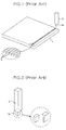
- Fig. 1 is a perspective view, showing a conventional method of manufacturing a plate punch used for forming the partition walls of plasma display panels.
- a cutting bite 2 linearly and repeatedly moves on the top surface of a forming plate 1 laid on a die (not shown), thus regularly and parallely forming a plurality of partition wall forming grooves 3 on the plate 1 and producing a desired plate punch.
- the tip 2a of the bite 2 has a vertical length equal to the desired height of each of the target partition walls and a width equal to the desired thickness of each target partition wall.
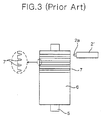
- the tip 2a of the bite may have two tapered shapes, and so the width of each partition wall forming groove 3 formed on the forming plate 1 is gradually enlarged in a direction from the bottom to the top of the groove 3.
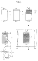
- Fig. 3 is a view, showing a conventional method of manufacturing a roll punch used for forming the partition walls on the rear panel of a plasma display panel.
- a cutting bite 2' having a tip 2a, forms a plurality of partition wall forming grooves 7 on the external surface of a forming roll 6 integrated with a rotating shaft 5 at its central axis, thus producing a desired roll punch.
- the conventional method of producing such a plate punch or a roll punch used for forming the partition walls on the rear panel of a PDP is problematic in that the tip 2a of the cutting bite 2 or 2' is gradually abraded, thus failing to form the partition wall forming grooves 3 having a desired shape or a desired surface smoothness.
- a desired strength of the bite 2 or 2' forces the shape of the tip 2a of the bite 2 or 2' to be undesirably limited. Due to such a limited shape of the tip 2a, it is very difficult to produce a variety of highly precise rear panels of PDPs.
- an object of the present invention is to provide a process of manufacturing a roll punch used for forming the partition walls on the rear panel of a PDP, which reduces the width of each partition wall forming groove formed on the external surface of a roll punch, and enlarges the width of each land between the forming grooves, thus allowing an easy arrangement of address electrodes on the rear panel of the PDP and enlarging the area of the light emitting part of the PDP, and which easily and simply produces a desired roll punch.
- the present invention provides a process of manufacturing a roll punch used for forming the partition walls of a plasma display panel, comprising the steps of: coating a mask on the external surface of a forming roll; partially removing the mask from the forming roll at regularly spaced positions while rotating the forming roll, thus forming an intermediate product having a plurality of regularly spaced mask-free parts; etching the intermediate product at the mask-free parts using ultrasonic waves within an etching tank provided with an ultrasonic vibrator, thus forming a plurality of partition wall forming grooves on the forming roll of the intermediate product; and completely removing the remaining part of the mask from the forming roll having the partition wall forming grooves, thus finally producing a desired roll punch.
- the inclination angle of each inclined sidewall of each of the partition wall forming grooves of the roll punch relative to a vertical reference line perpendicular to the external surface of lands between the forming grooves is 3° or less.
- partition wall forming grooves of the roll punch produced through the process of this invention are fabricated such that a value of [h/(b-a)] is 30 or more, wherein “h” is a height of each of the partition walls formed on the plasma display panel by the forming grooves of the roll punch, "b” is a width of the middle portion of the partition wall, and “a” is a width of the top portion of the partition wall.
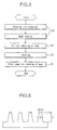
- Fig. 4 is a view, showing a process of manufacturing a roll punch used for forming the partition walls on the rear panel of a plasma display panel in accordance with the preferred embodiment of the present invention.
- Fig. 5 is a flowchart of the process of this invention.
- a forming roll 21 is concentrically mounted to a unidirectionally rotatable shaft 11 prior to coating a mask 22 on the external surface of the roll 21 at the first step S1.
- the mask 22 is partially removed from the forming roll 21 using a laser beam or a cutting bite 23 at regularly spaced positions, thus forming an intermediate product 25 having a plurality of regularly spaced mask-free parts where desired partition wall forming grooves 41 are to be formed at later step.
- the forming roll 21 is rotated in a direction.
- the intermediate product 25 from the second step S2 is, thereafter, sunk and fixed in an etching tank 30 at the third step S3.
- two ultrasonic vibrators 31a and 31b are placed within the etching tank 30 at opposite positions, and so the forming roll 21 of the intermediate product 25 is partially etched at the regularly spaced mask-free parts by ultrasonic waves radiated from the two ultrasonic vibrators 31a and 31b. Therefore, desired partition wall forming grooves 41 are formed on the forming roll 21 of the intermediate product 25 at the mask-free parts.
- the intermediate product 25 is removed from the etching tank 30 prior to completely removing the remaining mask 22 from the external surface of the forming roll 21 at the fourth step S4, thus finally producing a desired roll punch 40.
- the minus gradient that is, the inclination angle ⁇ of each inclined sidewall L2 of each forming groove 41 relative to a vertical reference line L1 perpendicular to the external surface of the lands 42 between the grooves 41 is 3° or less.
- Each partition wall formed on the rear panel of a PDP using the roll punch 40, has almost vertical sidewalls as shown in Fig. 6. That is, the value of [h/(b-a)] is 30 or more, wherein “h” is the height of each partition wall, “b” is the width of the middle portion of the partition wall, and “a” is the width of the top portion of the partition wall, and so each partition wall has almost vertical sidewalls.
- each land 42 of the roll punch 40 is enlarged in comparison with the conventional roll punches, and so it is possible to allow an easy arrangement of address electrodes on the rear panel of a PDT.
- the present invention provides a process of manufacturing a roll punch used for forming the partition walls on the rear panel of a PDP.
- a forming roll is primarily coated with a mask on its external surface. Thereafter, the mask is partially removed from the forming roll, thus forming a plurality of regularly spaced mask-free parts on the forming roll.
- the forming roll is, thereafter, etched at the mask-free parts using ultrasonic waves within an etching tank, and so a desired roll punch having partition wall forming grooves is produced.
- the roll punch manufacturing process of this invention thus enlarges the width of the lands between the forming grooves of the roll punch, thus allowing an easy arrangement of address electrodes on the rear panel of a PDP.
- the roll punch produced through the process of this invention, preferably enlarges the area of the light emitting part of a PDP by about 15% in comparison with conventional roll punches.
Landscapes
- Engineering & Computer Science (AREA)
- Manufacturing & Machinery (AREA)
- Gas-Filled Discharge Tubes (AREA)
- Laser Beam Processing (AREA)
- ing And Chemical Polishing (AREA)
Abstract
Description
Claims (5)
- A process of manufacturing a roll punch used for forming partition walls of a plasma display panel, comprising the steps of:coating a mask on an external surface of a forming roll;partially removing the mask from said forming roll at regularly spaced positions while rotating said forming roll, thus forming an intermediate product having a plurality of regularly spaced mask-free parts;etching said intermediate product at the mask-free parts using ultrasonic waves within an etching tank provided with an ultrasonic vibrator, thus forming a plurality of partition wall forming grooves on said forming roll of the intermediate product; andcompletely removing a remaining part of said mask from the forming roll having the partition wall forming grooves, thus finally producing a roll punch.
- The process according to claim 1, wherein the partial removal of said mask from the forming roll at the regularly spaced positions is carried out by radiating a laser beam on the mask.
- The process according to claim 1, wherein the partial removal of said mask from the forming roll at the regularly spaced positions is carried out by a cutting bite.
- The process according to claim 1, wherein an inclination angle of each inclined sidewall of each of said partition wall forming grooves of the roll punch relative to a vertical reference line perpendicular to an external surface of lands between said forming grooves is 3° or less.
- The process according to claim 1, wherein the partition wall forming grooves of the roll punch are fabricated such that a value of [h/(b-a)] is 30 or more, wherein "h" is a height of each of the partition walls formed on the plasma display panel by said forming grooves of the roll punch, "b" is a width of a middle portion of said partition wall, and "a" is a width of a top portion of said partition wall.
Applications Claiming Priority (2)
| Application Number | Priority Date | Filing Date | Title |
|---|---|---|---|
| KR1019990058733A KR100341841B1 (en) | 1999-12-17 | 1999-12-17 | A manufacturing method for barrier-rib forming of plasma display panel |
| KR9958733 | 1999-12-17 |
Publications (2)
| Publication Number | Publication Date |
|---|---|
| EP1109193A1 true EP1109193A1 (en) | 2001-06-20 |
| EP1109193B1 EP1109193B1 (en) | 2006-09-13 |
Family
ID=37068219
Family Applications (1)
| Application Number | Title | Priority Date | Filing Date |
|---|---|---|---|
| EP00126280A Expired - Lifetime EP1109193B1 (en) | 1999-12-17 | 2000-12-01 | Process of manufacturing roll punch used for forming partition walls of plasma display panel |
Country Status (5)
| Country | Link |
|---|---|
| US (1) | US20010004065A1 (en) |
| EP (1) | EP1109193B1 (en) |
| JP (1) | JP3289012B2 (en) |
| KR (1) | KR100341841B1 (en) |
| DE (1) | DE60030666T2 (en) |
Families Citing this family (5)
| Publication number | Priority date | Publication date | Assignee | Title |
|---|---|---|---|---|
| KR20030017244A (en) * | 2001-08-24 | 2003-03-03 | 주식회사 유피디 | Fabrication method of rolling mold for barrier rib in plasma display panel and method of forming barrier rib using the mold |
| GB0127410D0 (en) * | 2001-11-15 | 2002-01-09 | Renishaw Plc | Laser substrate treatment |
| KR101026659B1 (en) * | 2004-09-27 | 2011-04-04 | 아사히 가라스 가부시키가이샤 | Method for manufacturing electrode and / or black stripe for plasma display substrate |
| TWI251266B (en) * | 2005-03-11 | 2006-03-11 | Ind Tech Res Inst | Manufacturing method of the microstructure for roller and the structure thereof |
| DE102020108247A1 (en) | 2020-03-25 | 2021-09-30 | Trumpf Laser- Und Systemtechnik Gmbh | LARGE-VOLUME REMOVAL OF MATERIAL USING LASER-ASSISTED ETCHING |
Citations (4)
| Publication number | Priority date | Publication date | Assignee | Title |
|---|---|---|---|---|
| US5281511A (en) * | 1991-08-05 | 1994-01-25 | Gerhardt International A/S | Process for producing an embossing die in roll form |
| EP0836892A2 (en) * | 1996-10-21 | 1998-04-22 | Dai Nippon Printing Co., Ltd. | Transfer sheet, and pattern-forming method |
| US5853446A (en) * | 1996-04-16 | 1998-12-29 | Corning Incorporated | Method for forming glass rib structures |
| JPH11213918A (en) * | 1997-10-22 | 1999-08-06 | Hewlett Packard Co <Hp> | Flat-panel display device |
Family Cites Families (1)
| Publication number | Priority date | Publication date | Assignee | Title |
|---|---|---|---|---|
| US5747931A (en) * | 1996-05-24 | 1998-05-05 | David Sarnoff Research Center, Inc. | Plasma display and method of making same |
-
1999
- 1999-12-17 KR KR1019990058733A patent/KR100341841B1/en not_active Expired - Fee Related
-
2000
- 2000-12-01 DE DE60030666T patent/DE60030666T2/en not_active Expired - Fee Related
- 2000-12-01 EP EP00126280A patent/EP1109193B1/en not_active Expired - Lifetime
- 2000-12-05 JP JP2000369485A patent/JP3289012B2/en not_active Expired - Fee Related
- 2000-12-07 US US09/730,783 patent/US20010004065A1/en not_active Abandoned
Patent Citations (5)
| Publication number | Priority date | Publication date | Assignee | Title |
|---|---|---|---|---|
| US5281511A (en) * | 1991-08-05 | 1994-01-25 | Gerhardt International A/S | Process for producing an embossing die in roll form |
| US5853446A (en) * | 1996-04-16 | 1998-12-29 | Corning Incorporated | Method for forming glass rib structures |
| EP0836892A2 (en) * | 1996-10-21 | 1998-04-22 | Dai Nippon Printing Co., Ltd. | Transfer sheet, and pattern-forming method |
| JPH11213918A (en) * | 1997-10-22 | 1999-08-06 | Hewlett Packard Co <Hp> | Flat-panel display device |
| US6072274A (en) * | 1997-10-22 | 2000-06-06 | Hewlett-Packard Company | Molded plastic panel for flat panel displays |
Non-Patent Citations (1)
| Title |
|---|
| PATENT ABSTRACTS OF JAPAN vol. 1999, no. 13 30 November 1999 (1999-11-30) * |
Also Published As
| Publication number | Publication date |
|---|---|
| US20010004065A1 (en) | 2001-06-21 |
| JP2001234365A (en) | 2001-08-31 |
| DE60030666T2 (en) | 2007-10-18 |
| KR20010057010A (en) | 2001-07-04 |
| EP1109193B1 (en) | 2006-09-13 |
| JP3289012B2 (en) | 2002-06-04 |
| KR100341841B1 (en) | 2002-06-24 |
| DE60030666D1 (en) | 2006-10-26 |
Similar Documents
| Publication | Publication Date | Title |
|---|---|---|
| JPH07288087A (en) | Plasma display panel | |
| US6445125B1 (en) | Flat panel display having field emission cathode and manufacturing method thereof | |
| EP1109193A1 (en) | Process of manufacturing roll punch used for forming partition walls of plasma display panel | |
| EP1670022B1 (en) | Plasma display panel | |
| KR100324269B1 (en) | Plasma Display Panel for Radio Frequency | |
| US7564680B2 (en) | Display apparatus and method of combining chassis base with boss | |
| US7023136B2 (en) | Gas discharge panel and method of production of a gas discharge panel | |
| US7274144B2 (en) | Plasma display panel provided with electrode pairs bordering each sidewall of barrier ribs members | |
| US20080122356A1 (en) | Plasma display panel | |
| JP2953985B2 (en) | Sandblasting device and method for manufacturing gas discharge type display device | |
| US7230586B1 (en) | Radio frequency plasma display panel and fabricating method thereof and driving apparatus therefor | |
| US20080024064A1 (en) | Plasma display panel (PDP) | |
| US6783415B2 (en) | Method for forming ribs in a plasma display panel | |
| JP2006120633A (en) | Plasma display panel and its manufacturing method | |
| KR0142024B1 (en) | Method for manufacturing plasma display device and device | |
| JP2004014478A (en) | Plasma display panel | |
| US7812535B2 (en) | Plasma display panel | |
| KR100947150B1 (en) | Surface Discharge AC Plasma Display Panel for Multi Screen | |
| US7545346B2 (en) | Plasma display panel and a drive method therefor | |
| CN1303636C (en) | Improvement to colour cathode ray tubes | |
| JP2004014480A (en) | Plasma display panel | |
| KR20010065073A (en) | Fabrication of barrier rib for plasma display panel using rolling-press method | |
| JP2004014479A (en) | Plasma display panel | |
| KR20010073512A (en) | Plasma display panel | |
| US20040227463A1 (en) | Flat panel display having conductors magnetically bonded to substrate |
Legal Events
| Date | Code | Title | Description |
|---|---|---|---|
| PUAI | Public reference made under article 153(3) epc to a published international application that has entered the european phase |
Free format text: ORIGINAL CODE: 0009012 |
|
| AK | Designated contracting states |
Kind code of ref document: A1 Designated state(s): DE FR GB |
|
| AX | Request for extension of the european patent |
Free format text: AL;LT;LV;MK;RO;SI |
|
| 17P | Request for examination filed |
Effective date: 20010704 |
|
| AKX | Designation fees paid |
Free format text: DE FR GB |
|
| 17Q | First examination report despatched |
Effective date: 20031204 |
|
| GRAP | Despatch of communication of intention to grant a patent |
Free format text: ORIGINAL CODE: EPIDOSNIGR1 |
|
| GRAS | Grant fee paid |
Free format text: ORIGINAL CODE: EPIDOSNIGR3 |
|
| GRAA | (expected) grant |
Free format text: ORIGINAL CODE: 0009210 |
|
| AK | Designated contracting states |
Kind code of ref document: B1 Designated state(s): DE FR GB |
|
| REG | Reference to a national code |
Ref country code: GB Ref legal event code: FG4D |
|
| REF | Corresponds to: |
Ref document number: 60030666 Country of ref document: DE Date of ref document: 20061026 Kind code of ref document: P |
|
| ET | Fr: translation filed | ||
| PLBE | No opposition filed within time limit |
Free format text: ORIGINAL CODE: 0009261 |
|
| STAA | Information on the status of an ep patent application or granted ep patent |
Free format text: STATUS: NO OPPOSITION FILED WITHIN TIME LIMIT |
|
| 26N | No opposition filed |
Effective date: 20070614 |
|
| PGFP | Annual fee paid to national office [announced via postgrant information from national office to epo] |
Ref country code: GB Payment date: 20071128 Year of fee payment: 8 Ref country code: FR Payment date: 20071210 Year of fee payment: 8 |
|
| PGFP | Annual fee paid to national office [announced via postgrant information from national office to epo] |
Ref country code: DE Payment date: 20071129 Year of fee payment: 8 |
|
| GBPC | Gb: european patent ceased through non-payment of renewal fee |
Effective date: 20081201 |
|
| REG | Reference to a national code |
Ref country code: FR Ref legal event code: ST Effective date: 20090831 |
|
| PG25 | Lapsed in a contracting state [announced via postgrant information from national office to epo] |
Ref country code: DE Free format text: LAPSE BECAUSE OF NON-PAYMENT OF DUE FEES Effective date: 20090701 |
|
| PG25 | Lapsed in a contracting state [announced via postgrant information from national office to epo] |
Ref country code: GB Free format text: LAPSE BECAUSE OF NON-PAYMENT OF DUE FEES Effective date: 20081201 |
|
| PG25 | Lapsed in a contracting state [announced via postgrant information from national office to epo] |
Ref country code: FR Free format text: LAPSE BECAUSE OF NON-PAYMENT OF DUE FEES Effective date: 20081231 |