EP1106995A2 - Laser beam inspection apparatus - Google Patents
Laser beam inspection apparatus Download PDFInfo
- Publication number
- EP1106995A2 EP1106995A2 EP00310586A EP00310586A EP1106995A2 EP 1106995 A2 EP1106995 A2 EP 1106995A2 EP 00310586 A EP00310586 A EP 00310586A EP 00310586 A EP00310586 A EP 00310586A EP 1106995 A2 EP1106995 A2 EP 1106995A2
- Authority
- EP
- European Patent Office
- Prior art keywords
- scan
- laser beam
- inspection apparatus
- refracting members
- objects
- Prior art date
- Legal status (The legal status is an assumption and is not a legal conclusion. Google has not performed a legal analysis and makes no representation as to the accuracy of the status listed.)
- Granted
Links
Images



Classifications
-
- G—PHYSICS
- G01—MEASURING; TESTING
- G01N—INVESTIGATING OR ANALYSING MATERIALS BY DETERMINING THEIR CHEMICAL OR PHYSICAL PROPERTIES
- G01N21/00—Investigating or analysing materials by the use of optical means, i.e. using sub-millimetre waves, infrared, visible or ultraviolet light
- G01N21/84—Systems specially adapted for particular applications
- G01N21/88—Investigating the presence of flaws or contamination
- G01N21/95—Investigating the presence of flaws or contamination characterised by the material or shape of the object to be examined
- G01N21/956—Inspecting patterns on the surface of objects
- G01N21/95684—Patterns showing highly reflecting parts, e.g. metallic elements
Definitions
- the present invention relates generally to a laser beam inspection apparatus which inspects an electronic parts-fabricated substrate for defects, and more particularly to a laser beam inspection apparatus designed to monitor whether electronic parts or components are mounted in desired positions on a substrate or not and whether they are correct ones or not.
- Typical inspection apparatuses of the above type include a laser emitter radiating a laser beam onto each electronic component such as an IC mounted on a substrate, a laser receiver receiving a return of the laser beam from the electronic component, and an inspection circuit processing the return of the laser beam to obtain information about the appearance of the electronic component.
- the inspection apparatuses of this type are designed to obtain the appearance information on the electronic components using triangulation.
- the above inspection apparatuses have a drawback in that an inspection error may arise when the size of the electronic components is changed.
- the inspection apparatus first fixes a scan range in which a laser beam is to be radiated onto the substrate and then scans the laser beam in the scan range to determine the size of a target one of the electronic components and whether the target electronic component is mounted in a correct orientation or not. Therefore, in a case where a larger electronic component is inspected in the scan range which was determined when a smaller electronic component was inspected in a previous cycle, it may become impossible to scan the whole of an area of the larger electronic component including the tolerance, which leads to the inspection error.
- an inspection apparatus which comprises: (a) a laser emitter emitting a laser beam for inspecting objects; (b) a scan mechanism moving the laser beam emitted from the laser emitter to scan a target one of the objects in a given scan range, the scan mechanism being designed to change orientation of emission of the laser beam to change the scan range; and (c) a laser receiver receiving a return of the laser beam from the target object to provide an object-inspected data.
- the invention can provide an inspection apparatus capable of changing orientation of a scan of a laser beam and/or an area of a scan range as a function of the type of a target object to be inspected.
- the scan mechanism includes refracting members arranged adjacent each other along an optical path of the laser beam emitted from the laser emitter.
- the refracting members may be made of flat plates.
- the scan mechanism works to rotate the refracting members in the same direction about a given axis of rotation to achieve circular scanning of the laser beam.
- the scan mechanism holds a given relative angle between the refracting members and rotates the refracting members to achieve the circular scanning of the laser beam in the scan range.
- the scan mechanism includes an angle changing mechanism designed to change the relative angle between the refracting members to change the scan range and rotates the refracting members while keeping the relative angle to achieve the circular scanning of the laser beam in the changed scan range.
- the angle changing mechanism changes a speed of rotation of one of the refracting members to change the scan range.
- a moving mechanism is further provided which is designed to move the inspection apparatus from one of the objects to another having a different size after completion of a scan of the one of the objects.
- the angle changing mechanism changes the relative angle between the refracting members during movement of the inspection apparatus.
- the scan mechanism may rotate the refracting members in opposite directions synchronously about the given axis of rotation to achieve rectilinear scanning of the laser beam in which a spot of the laser beam moves along a straight scan path.
- the angle changing mechanism changes the relative angle between the refracting members to change orientation of the rectilinear scanning.
- the objects to be inspected may be electronic components each made up of a body and a lead extending from the body.
- the scan mechanism rotates the refracting members made up of flat plates in the same direction synchronously about the given axis of rotation to achieve the circular scanning of the laser beam when the body of each of the electronic components is inspected.
- the angle changing mechanism changes and keeps the relative angle between the refracting members at 180° to achieve movement of the laser beam linearly when the lead is inspected.
- the angle changing mechanism may change and rotate the refracting members in the opposite directions synchronously while keeping the relative angle between the refracting members at a given value to perform the rectilinear scanning of the laser beam when the lead is inspected.
- an inspection apparatus which comprises: (a) a laser emitter emitting a laser beam for inspecting objects; (b) a scan mechanism subjecting the laser beam emitted from the laser emitter to circular motion to scan a target one of the objects in a circular scan range cyclically, the scan mechanism being designed to control orientation of emission of the laser beam to determine an area of the circular scan range as a function of the size of the target object; and (c) a laser receiver receiving a return of the laser beam from the target object to provide an object-inspected data.
- an inspection apparatus which comprises: (a) a laser emitter emitting a laser beam for inspecting objects; (b) a scan mechanism including refracting members disposed adjacent to each other along an optical path of the laser beam to change orientation of emission of the laser beam emitted from the laser emitter to perform rectilinear scanning about a target one of the objects, the scan mechanism being designed to change a relative angle between the refracting members to change orientation of the rectilinear scanning of the laser beam as a function of orientation of the target object; and (c) a laser receiver receiving a return of the laser beam from the target object to provide an object-inspected data.
- a laser beam inspection apparatus which is designed to monitor whether electronic components are each mounted in a desired position on a substrate or not and whether they are correct ones or not.
- the inspection apparatus includes a body 1, a sensor head 2, a set of flat glass plates 5 and 6 (i.e., refracting members), servomotors 9 and 10, and a moving mechanism 70.
- the sensor head 2 has disposed therein a laser emitter 3 and a laser receiver 4.
- the glass plates 5 and 6 are disposed beneath the laser head 2 and arranged adjacent each other at a given interval along an optical path of a laser beam emitted from the laser emitter 3.
- the glass plates 5 and 6 are supported by the body 1 rotatably and connected to the servomotors 9 and 10 through timing belts 7 and 8, respectively.
- the moving mechanism 70 includes, for example, an XY table designed to move the body 1 horizontally and vertically on a plane.
- a substrate 11 Placed beneath the inspection apparatus is a substrate 11 on which a plurality of circuit components 12 are mounted.
- Fig. 3 shows an example of electronic components mounted on the substrate 11.
- the electronic component 12a is the largest in size.
- the electronic component 12b is the second largest.
- the electronic component 12d is the smallest.
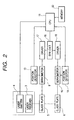
- Fig. 2 shows a circuit structure of the inspection apparatus.
- the servomotors 9 and 10 are coupled with position detectors (e.g., encoders) 13 and 14, respectively.
- the laser emitter 3 includes, for example, a semiconductor laser.
- the laser receiver 4 includes, for example, a light-sensitive element.
- the laser receiver 4 and the position detectors 13 and 14 are coupled with a CPU 15. Specifically, the position detectors 13 and 14 monitor angular positions of the servomotors 9 and 10 and output position signals indicative thereof to the CPU 15, respectively.
- the servomotors 9 and 10 are, as described above, connected to the glass plates 5 and 6 through the timing belts 9 and 10 and to motor drivers 17 and 18, respectively.
- the motor drivers 17 and 18 usually rotate the servomotors 9 and 10 synchronously through a synchronization circuit 16, but either of the motor drivers 17 and 18 is controlled by the CPU 15 to change the speed of a corresponding one of the servomotors 9 and 10 temporarily to establish, as shown in Figs. 4(a), 4(b), and 4(c), three angular relations between the glass plates 5 and 6.
- the CPU 15 provides a synchronization disable signal to the synchronization circuit 16 to disable the synchronization of the servomotors 9 and 10 and increases or decreases the speed of one of the glass plates 5 and 6 to establish a desired angular relation between the glass plates 5 and 6.
- Fig. 4(a) illustrates for the case where surfaces of the glass plates 5 and 6 are in parallel to each other, which will be referred to below as a relative angle of zero (0° ).
- Fig. 4(b) illustrates for the case where the surfaces of the glass plates 5 and 6 are oriented in different directions at a relative angle of 90° .
- Fig. 4(d) shows a scan locus of a laser beam in the case of Fig. 4(b).
- r1 indicates the radius of a rotational path of the glass plate 5.
- r2 indicates the radius of a rotational path of the glass plate 6.
- ⁇ indicated the relative angle between the glass plates 5 and 6.
- a solid line indicates a scan locus of a laser beam passing through the glass plates 5 and 6.
- a laser beam emitted from the laser emitter 3 scans, as shown in the lower side of Fig. 4(b), along a circle smaller than the one shown in Fig. 4(a).
- Fig. 4(c ) illustrates for the case where the glass plates 5 and 6 are oriented in opposite directions at a relative angle of 180° .
- This positional relation is achieved by disenabling the synchronization circuit 16, changing one of the glass plates 5 and 6, and stopping the one of the glass plates 5 and 6 after it have rotated 90° from the status of Fig. 4(b) or 180° from the status of Fig. 4(a).
- a laser beam emitted from the laser emitter 3 forms a spot, as shown in the lower side of Fig. 4(c).
- Figs. 5(a), 5(b), and 5(c) show one example of a relation between speed control of the servomotors 10 and 9 and the relative angle between the glass plates 5 and 6.
- the servomotors 10 and 9 are first controlled by the motor drivers 18 and 17 so that they rotate at the same speed A0 with the glass plates 5 and 6 oriented at a relative angle ⁇ 0 of 0° .
- the motor driver 18 decreases the speed of the servomotor 10 to rotate the servomotor 10 at a speed A1 for a time period of T1 until a relative angle ⁇ 2 of 180° is reached and then returns the speed of the servomotor 10 to A0.
- the motor driver 18 increases the speed of the servomotor 10 to rotate the servomotor 10 at a speed of A2 for a time period of T2 until a relative angle ⁇ 1 of 90° is reached and then returns the speed of the servomotor 10 back to A0.
- the motor driver 18 decreases the speed of the servomotor 10 to rotate the servomotor 10 at a speed A3 for a time period of T3 until a relative angle ⁇ 2 of 180° is reached and then returns the speed of the servomotor 10 to A0.
- time periods T1, T2, and T3 may either be equal to or different from each other.
- the speeds A1, A2, and A3 of the servomotor 10 may be changed to establish desired relative angles between the glass plates 5 and 6, respectively.
- the time periods T1, T2, and T3 may be set different from each other.
- the CPU 15 may control the speed of either or both of the servomotors 9 and 10 to change the angle between the glass plates 5 and 6 to a desired one, thereby modifying an area of a scan range of a laser beam emitted from the sensor head 2.
- the inspection apparatus When the inspection apparatus is moved to the right, as viewed in Fig. 1, by the moving mechanism 70 while keeping the relative angle between the glass plates 5 and 6 at a desired one, it will cause a laser beam to travel to the right, as shown in a lower side of the drawing, while scanning the surface of the substrate 11 along circles of a desired size.
- the CPU 15 moves the inspection apparatus horizontally and rotates the servomotors 9 and 10 synchronously at the same speed while keeping the relative angle between the glass plates 5 and 6 at zero (0° ), thereby causing a laser beam to scan the largest electronic component 12a along the largest circles.
- the CPU 15 confirms the location and size of the electronic component 12c to be inspected next by look-up using data stored in the memory 60 installed in the inspection apparatus and adjusts the relative angle between the glass plates 5 and 6 to, for example, 160° to change the scan range to one predetermined as a function of the size of the electronic component 12c.
- the CPU 15 moves the inspection apparatus upward to the electronic component 12c through the moving mechanism 70 and starts a scan of the electronic component 12c in the smallest scan range.
- the adjustment of the relative angle between the glass plates 5 and 6 may be made during movement of the inspection apparatus to the electronic component 12c.
- the CPU 15 confirms the location and size of the electronic component 12b to be inspected next by look-up using data stored in the memory and adjusts the relative angle between the glass plates 5 and 6 to, for example, 100° to change the scan range to one predetermined as a function of the size of the electronic component 12b.
- the CPU 15 moves the inspection apparatus horizontally to the electronic component 12b through the moving mechanism 70 and starts a scan of the electronic component 12b in the middle sized-scan range. After completion of a given number of scans of the electronic component 12b, the CPU 15 confirms the location and size of the electronic component 12c to be inspected next by look-up using data stored in the memory and adjusts the relative angle between the glass plates 5 and 6 to 160° that is identical with that in the second scan. The CPU 15 then moves the inspection apparatus horizontally and starts a scan of the electronic component 12c.
- the inspection apparatus of this embodiment is, as apparent from the above discussion, capable of changing the scan range as a function of the size of an electronic component to be inspected, thereby minimizing inspection errors.
- the electronic components 12a to 12c are different in size from each other and have different tolerances in mounting on the substrate 11.
- the optimum scan ranges for inspecting the electronic components 12a to 12c are, therefore, different in area from each other. If the largest electronic component 12a is scanned in the smallest scan range for the electronic component 12c, it may result in an error in detecting the presence of the electronic component 12a. Conversely, if the smallest electronic component 12c is scanned in the largest scan range, it will consume time more than required, thus resulting in an increase in total time for inspection of the electronic components 12a to 12c.
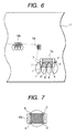
- the laser beam scans each of the electronic components 12a to 12c four cycles regardless of the size of the electronic components 12a to 12c.
- the laser beam as shown in Fig. 6, first runs on the electronic component 12a from the substrate 11 at point a and then drops to the substrate at point b.
- the laser beam runs on the electronic component 12a again at point c and drops to the substrate 11 at point d.
- Such a scan cycle is further repeated two times.
- the laser beam last drops to the substrate 11 from the electronic component 12a at point j.
- four scans are performed to sample ten data on the electronic component 12a.
- the laser receiver 4 receives and converts a return of the laser beam from the substrate 11 into an electric signal and outputs it to the CPU 15.
- the CPU 15 picks up the sampled data from the signal outputted from the laser receiver 4 and compares them with reference data stored in the memory 60 to determine, for example, the size and orientation of the electronic component 12a, thereby determining whether the electronic component 12a is mounted on the substrate 11 in a correct position or not and whether the electronic component 12a is a desired one or not.
- Fig. 7 shows a modification of the above first embodiment.
- the inspection apparatus first moves to the electronic component 12a on the substrate 11 and stops above it.
- the laser emitter 3 radiates a laser beam to scan the electronic component 12a only one cycle.
- the glass plates 5 and 6 are turned one cycle in the angular relation as shown in Fig. 4(a).
- the scanning of the electronic component 12a in a circular range whose radius is smaller than the length of the electronic component 12a enables four data on the electronic component 12a to be sampled at points A, B , C, and D. This results in decrease in accuracy of the inspection, but allows the time required to inspect each electronic component to be decreased as compared with the above embodiment. This modification is, thus, applicable to the case where the mounting accuracy is not so critical.
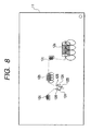
- Fig. 8 illustrates a scan path of the laser beam in a case where it is required to check whether three terminal pins 12 B of an electronic component 12d are mounted on the substrate 11 correctly or not as well as inspecting the electronic components 12a to 12c mounted on the substrate 11.
- the terminal pins 12 B project outward from a body 12 A of the electronic component 12d.
- the CPU 15 adjusts the relative angle between the glass plates 5 and 6 to 180° , as shown in Fig. 4(c), to change the circular scan range to a spot one and moves the laser beam along a broken line, as indicated in Fig. 8, scan the three terminal pins 12B. This enables the inspection of small parts without stopping the rotation of the glass plates 5 and 6 or changing the relative angle therebetween to decrease the scan range.
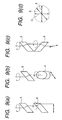
- the inspection apparatus may alternatively rotate the glass plates 5 and 6 in opposite directions in the above embodiments to achieve rectilinear scanning in which the laser beam moves along a straight scan path, thereby allowing leads of small electronic parts such as ICs, which are difficult to detect with the circular scanning, to be inspected at high speeds.
- Fig. 9(a) illustrates the glass plates 5 and 6 which are held at a relative angle of zero (0° ). Rotating the glass plates 5 and 6 synchronously in opposite directions causes a laser beam emitted from the laser emitter 3 to move along a straight scan path, as indicated by A in Fig. 9(d), extending horizontally, as viewed in the drawing.
- Fig. 9(b) illustrates the glass plates 5 and 6 which are held at a relative angle of 90° .
- Rotating the glass plates 5 and 6 synchronously in opposite directions causes a laser beam emitted from the laser emitter 3 to move along a straight scan path, as indicated by B in Fig. 9(d), extending at 45° to the scan path A.
- Fig. 9(c ) illustrates the glass plates 5 and 6 which are held at a relative angle of 180° .
- Rotating the glass plates 5 and 6 synchronously in opposite directions causes a laser beam emitted from the laser emitter 3 to move along a straight scan path, as indicated by C in Fig. 9(d), extending at 90° to the scan path A .
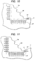
- Fig. 10 shows an example of inspecting electronic components mounted on the substrate 11 with the above described straight scanning.
- the substrate 11 has disposed thereon a plurality of ICs 12e (one is shown for the brevity of illustration)
- the IC 12e has a plurality of leads 12F extending outward from the periphery of a body 12 E .
- the moving mechanism 70 moves the body 1 of the inspection apparatus around the IC 12e along a broken line A as shown in Fig. 10.
- the moving mechanism 70 stops the body 1 above one of the leads 12F which extends horizontally as viewed in the drawing.
- the CPU 15 adjusts the relative angle between the glass plate 5 and 6 to zero (0° ), as shown in Fig. 9(a), and rotates the glass plates 5 and 6 synchronously in opposite directions, thereby causing the laser beam to move horizontally along the scan path A shown in Fig. 9(d).
- the laser beam traverses the length of the lead 12e, thus allowing the CPU 15 to determine whether the lead 12 F is mounted on the substrate 11 in a correct position or not.
- the moving mechanism 70 moves the body 1 to a rightmost one of the lower array of the leads 12 F and stops above it.
- the CPU 15 adjusts the relative angle between the glass plate 5 and 6 to 180° , as shown in Fig. 9(c), and rotates the glass plates 5 and 6 synchronously in opposite directions, thereby causing the laser beam to move vertically along the scan path C shown in Fig. 9(d). Specifically, the laser beam traverses the length of the lead 12F, thus allowing the CPU 15 to determine whether the lead 12F is mounted on the substrate 11 in a correct position or not.
- Fig. 11 shows a comparative example of inspecting the leads 12F through the circular scanning where the glass plates 5 and 6 are held at a relative angle of 180° .
- complete inspection of all the leads 12 F requires the laser beam to move along a zigzag broken line B , which results in an increase in total length of the scan path, thus leading to a reduction in inspection speed.
Landscapes
- Physics & Mathematics (AREA)
- Health & Medical Sciences (AREA)
- Life Sciences & Earth Sciences (AREA)
- Chemical & Material Sciences (AREA)
- Analytical Chemistry (AREA)
- Biochemistry (AREA)
- General Health & Medical Sciences (AREA)
- General Physics & Mathematics (AREA)
- Immunology (AREA)
- Pathology (AREA)
- Investigating Materials By The Use Of Optical Means Adapted For Particular Applications (AREA)
- Length Measuring Devices By Optical Means (AREA)
Abstract
Description
Claims (18)
- An inspection apparatus comprising:a laser emitter for emitting a laser beam for inspecting objects;a scan mechanism for moving the laser beam emitted from said laser emitter to scan a target one of the objects in a given scan range, said scan mechanism being designed to change orientation of emission of the laser beam to change the scan range; anda laser receiver receiving a return of the laser beam from the target object to provide an object-inspected data.
- An inspection apparatus as set forth in claim 1, wherein said scan mechanism includes refracting members arranged adjacent each other along an optical path of the laser beam emitted from said laser emitter.
- An inspection apparatus as set forth in claim 2, wherein the refracting members are made of flat plates.
- An inspection apparatus as set forth in claim 2 or 3, wherein said scan mechanism rotates the refracting members in the same direction about a given axis of rotation to achieve circular scanning of the laser beam.
- An inspection apparatus as set forth in claim 4, wherein said scan mechanism holds a given relative angle between the refracting members and rotates the refracting members to achieve the circular scanning of the laser beam in the scan range.
- An inspection apparatus as set forth in claim 5, wherein said scan mechanism includes an angle changing mechanism designed to change the relative angle between the refracting members to change the scan range and rotates the refracting members while keeping the relative angle to achieve the circular scanning of the laser beam in the changed scan range.
- An inspection apparatus as set forth in claim 6, wherein said angle changing mechanism changes a speed of rotation of one of the refracting members to change the scan range.
- An inspection apparatus as set forth in claim 6 or 7, further comprising a moving mechanism designed to move the inspection apparatus from one of the objects to another having a different size after completion of a scan of the one of the objects, and wherein said angle changing mechanism changes the relative angle between the refracting members during movement of the inspection apparatus.
- An inspection apparatus as set forth in claim 2 or 3, wherein said scan mechanism rotates the refracting members in opposite directions synchronously about a given axis of rotation to achieve rectilinear scanning of the laser beam in which a spot of the laser beam moves along a straight scan path.
- An inspection apparatus as set forth in claim 9, wherein said scan mechanism includes an angle changing mechanism designed to change the relative angle between the refracting members to change orientation of the rectilinear scanning.
- An inspection apparatus as set forth in claim 10, wherein said angle changing mechanism changes a speed of rotation of one of the refracting members to change the relative angle between the refracting members.
- An inspection apparatus as set forth in claim 11, further comprising a moving mechanism designed to move the inspection apparatus from one of the objects to another having a different size after completion of a scan of the one of the objects, and wherein said angle changing mechanism changes the relative angle between the refracting members during movement of the inspection apparatus.
- An inspection apparatus as set forth in claim 6, wherein the objects to be inspected are electronic components each made up of a body and a lead extending from the body, and wherein said scan mechanism rotates the refracting members made up of flat plates in the same direction synchronously about the given axis of rotation to achieve the circular scanning of the laser beam when the body of each of the electronic components is inspected, and said angle changing mechanism changes and keeps the relative angle between the refracting members at 180° to achieve movement of the laser beam linearly when the lead is inspected.
- An inspection apparatus as set forth in claim 13, further comprising a moving mechanism designed to move the inspection apparatus from one of the objects to another having a different size after completion of a scan of the one of the objects, and wherein said angle changing mechanism changes the relative angle between the refracting members during movement of the inspection apparatus.
- An inspection apparatus as set forth in claim 10, wherein the objects to be inspected are electronic components each made up of a body and a lead extending from the body, and wherein said scan mechanism rotates the refracting members made up of flat plates synchronously in the same direction about the given axis of rotation to achieve circular scanning of the laser beam when the body of each of the electronic components is inspected, and said angle changing mechanism changes and rotates the refracting members in the opposite directions synchronously while keeping the relative angle between the refracting members at a given value to perform the rectilinear scanning of the laser beam when the lead is inspected.
- An inspection apparatus as set forth in claim 15, further comprising a moving mechanism designed to move the inspection apparatus from one of the objects to another having a different size after completion of a scan of the one of the objects, and wherein said angle changing mechanism changes the relative angle between the refracting members during movement of the inspection apparatus.
- An inspection apparatus comprising:a laser emitter emitting a laser beam for inspecting objects;a scan mechanism subjecting the laser beam emitted from said laser emitter to circular motion to scan a target one of the objects in a circular scan range cyclically, said scan mechanism being designed to control orientation of emission of the laser beam to determine an area of the circular scan range as a function of the size of the target object; anda laser receiver receiving a return of the laser beam from the target object to provide an object-inspected data.
- An inspection apparatus comprising:a laser emitter emitting a laser beam for inspecting objects;a scan mechanism including refracting members disposed adjacent to each other along an optical path of the laser beam to change orientation of emission of the laser beam emitted from said laser emitter to perform rectilinear scanning about a target one of the objects, said scan mechanism being designed to change a relative angle between the refracting members to change orientation of the rectilinear scanning of the laser beam as a function of orientation of the target object; anda laser receiver receiving a return of the laser beam from the target object to provide an object-inspected data.
Applications Claiming Priority (4)
| Application Number | Priority Date | Filing Date | Title |
|---|---|---|---|
| JP34448299 | 1999-12-03 | ||
| JP34448299 | 1999-12-03 | ||
| JP2000326605 | 2000-10-26 | ||
| JP2000326605 | 2000-10-26 |
Publications (3)
| Publication Number | Publication Date |
|---|---|
| EP1106995A2 true EP1106995A2 (en) | 2001-06-13 |
| EP1106995A3 EP1106995A3 (en) | 2003-01-15 |
| EP1106995B1 EP1106995B1 (en) | 2004-08-04 |
Family
ID=26577780
Family Applications (1)
| Application Number | Title | Priority Date | Filing Date |
|---|---|---|---|
| EP00310586A Expired - Lifetime EP1106995B1 (en) | 1999-12-03 | 2000-11-29 | Laser beam inspection apparatus |
Country Status (4)
| Country | Link |
|---|---|
| US (1) | US6618135B2 (en) |
| EP (1) | EP1106995B1 (en) |
| CN (1) | CN1173167C (en) |
| DE (1) | DE60012672T2 (en) |
Families Citing this family (6)
| Publication number | Priority date | Publication date | Assignee | Title |
|---|---|---|---|---|
| DE60012672T2 (en) * | 1999-12-03 | 2005-08-11 | Matsushita Electric Industrial Co., Ltd., Kadoma | Tester with laser beam |
| US20150300962A1 (en) * | 2014-04-16 | 2015-10-22 | Texas Instruments Incorporated | Assembly For Inspecting Machine Parts Used In The Production Of Semiconductor Components |
| CN104931507B (en) * | 2015-06-05 | 2017-11-21 | 天津大学 | A kind of phone housing edge quality detecting system and detection method |
| DE102016220431A1 (en) * | 2016-10-18 | 2018-04-19 | Bielomatik Leuze Gmbh + Co. Kg | Method for heating an object and heating device |
| CN106483578B (en) * | 2016-11-25 | 2019-03-29 | 同方威视技术股份有限公司 | Mobile scanning-detecting system |
| ES2910779T3 (en) * | 2017-12-20 | 2022-05-13 | Fundacion Tecnalia Res & Innovation | Methods and systems for visual inspection |
Family Cites Families (9)
| Publication number | Priority date | Publication date | Assignee | Title |
|---|---|---|---|---|
| US4240750A (en) * | 1978-10-02 | 1980-12-23 | Hurd William A | Automatic circuit board tester |
| US4796997A (en) * | 1986-05-27 | 1989-01-10 | Synthetic Vision Systems, Inc. | Method and system for high-speed, 3-D imaging of an object at a vision station |
| US4963017A (en) * | 1989-05-01 | 1990-10-16 | General Electric Company | Variable depth range camera |
| US5192983A (en) * | 1989-12-19 | 1993-03-09 | Matsushita Electric Industrial Co., Ltd. | Apparatus for and method of checking external appearance of soldering state |
| US5020901A (en) * | 1990-01-30 | 1991-06-04 | The Perkin-Elmer Corporation | Multimode laser diode system for range measurement |
| US5082362A (en) * | 1990-07-02 | 1992-01-21 | General Electric Company | Zoom lens for a variable depth range camera |
| US5483337A (en) * | 1994-10-19 | 1996-01-09 | Barnard; Thomas W. | Spectrometer with selectable radiation from induction plasma light source |
| JPH08201757A (en) * | 1995-01-30 | 1996-08-09 | A G Technol Kk | Projection type color display device |
| DE60012672T2 (en) * | 1999-12-03 | 2005-08-11 | Matsushita Electric Industrial Co., Ltd., Kadoma | Tester with laser beam |
-
2000
- 2000-11-29 DE DE60012672T patent/DE60012672T2/en not_active Expired - Lifetime
- 2000-11-29 EP EP00310586A patent/EP1106995B1/en not_active Expired - Lifetime
- 2000-12-01 US US09/726,596 patent/US6618135B2/en not_active Expired - Fee Related
- 2000-12-04 CN CNB001352172A patent/CN1173167C/en not_active Expired - Fee Related
Also Published As
| Publication number | Publication date |
|---|---|
| CN1299049A (en) | 2001-06-13 |
| CN1173167C (en) | 2004-10-27 |
| US6618135B2 (en) | 2003-09-09 |
| EP1106995B1 (en) | 2004-08-04 |
| EP1106995A3 (en) | 2003-01-15 |
| DE60012672D1 (en) | 2004-09-09 |
| US20010002861A1 (en) | 2001-06-07 |
| DE60012672T2 (en) | 2005-08-11 |
Similar Documents
| Publication | Publication Date | Title |
|---|---|---|
| US4978224A (en) | Method of and apparatus for inspecting mounting of chip components | |
| KR100618558B1 (en) | Wafer prealignment device, wafer presence determination method, wafer edge position detection method and computer readable recording medium recording program for executing the method, wafer edge position detection device and prealignment sensor | |
| KR100318875B1 (en) | Electronic component mounting apparatus | |
| CN1235057C (en) | Testing device for printed boards | |
| US20110175997A1 (en) | High speed optical inspection system with multiple illumination imagery | |
| EP0606083B1 (en) | Exterior view inspecting apparatus for circuit board | |
| WO2011037903A1 (en) | High speed optical inspection system with camera array and compact, integrated illuminator | |
| WO2009094489A1 (en) | High speed optical inspection system with multiple illumination imagery | |
| EP1106995B1 (en) | Laser beam inspection apparatus | |
| JPH10261900A (en) | Inspection method for mounted components | |
| JP3266524B2 (en) | Chip component position detection method and device | |
| US5017864A (en) | Apparatus for the inspection of printed circuit boards on which components have been mounted | |
| JP3991729B2 (en) | Inspection device | |
| JP3258607B2 (en) | Surface inspection equipment | |
| WO2011056976A1 (en) | High speed optical inspection system with adaptive focusing | |
| JP2001153640A (en) | Printed circuit board inspection device | |
| JP2676780B2 (en) | Semiconductor device lead bending inspection device | |
| JP3203852B2 (en) | Inspection device for mounted printed circuit boards | |
| JP2002202269A (en) | Inspection equipment | |
| JPH06308530A (en) | Device for inspecting substrate | |
| JPS6157869A (en) | Inspecting device for printed wiring circuit | |
| JP2988594B2 (en) | Wafer center detection device | |
| JPH0555332A (en) | Foreign matter inspecting device | |
| JP3247920B2 (en) | Control method of electronic component mounting device | |
| JPH0672776B2 (en) | Inspection device for mounted printed circuit boards |
Legal Events
| Date | Code | Title | Description |
|---|---|---|---|
| PUAI | Public reference made under article 153(3) epc to a published international application that has entered the european phase |
Free format text: ORIGINAL CODE: 0009012 |
|
| AK | Designated contracting states |
Kind code of ref document: A2 Designated state(s): AT BE CH CY DE DK ES FI FR GB GR IE IT LI LU MC NL PT SE TR |
|
| AX | Request for extension of the european patent |
Free format text: AL;LT;LV;MK;RO;SI |
|
| PUAL | Search report despatched |
Free format text: ORIGINAL CODE: 0009013 |
|
| AK | Designated contracting states |
Kind code of ref document: A3 Designated state(s): AT BE CH CY DE DK ES FI FR GB GR IE IT LI LU MC NL PT SE TR |
|
| AX | Request for extension of the european patent |
Free format text: AL;LT;LV;MK;RO;SI |
|
| 17P | Request for examination filed |
Effective date: 20030505 |
|
| AKX | Designation fees paid |
Designated state(s): DE FR GB |
|
| 17Q | First examination report despatched |
Effective date: 20030825 |
|
| GRAP | Despatch of communication of intention to grant a patent |
Free format text: ORIGINAL CODE: EPIDOSNIGR1 |
|
| GRAS | Grant fee paid |
Free format text: ORIGINAL CODE: EPIDOSNIGR3 |
|
| GRAA | (expected) grant |
Free format text: ORIGINAL CODE: 0009210 |
|
| AK | Designated contracting states |
Kind code of ref document: B1 Designated state(s): DE FR GB |
|
| REG | Reference to a national code |
Ref country code: GB Ref legal event code: FG4D |
|
| REG | Reference to a national code |
Ref country code: IE Ref legal event code: FG4D |
|
| REF | Corresponds to: |
Ref document number: 60012672 Country of ref document: DE Date of ref document: 20040909 Kind code of ref document: P |
|
| ET | Fr: translation filed | ||
| PLBE | No opposition filed within time limit |
Free format text: ORIGINAL CODE: 0009261 |
|
| STAA | Information on the status of an ep patent application or granted ep patent |
Free format text: STATUS: NO OPPOSITION FILED WITHIN TIME LIMIT |
|
| 26N | No opposition filed |
Effective date: 20050506 |
|
| PGFP | Annual fee paid to national office [announced via postgrant information from national office to epo] |
Ref country code: FR Payment date: 20061108 Year of fee payment: 7 |
|
| PGFP | Annual fee paid to national office [announced via postgrant information from national office to epo] |
Ref country code: GB Payment date: 20061129 Year of fee payment: 7 |
|
| GBPC | Gb: european patent ceased through non-payment of renewal fee |
Effective date: 20071129 |
|
| REG | Reference to a national code |
Ref country code: FR Ref legal event code: ST Effective date: 20080930 |
|
| PG25 | Lapsed in a contracting state [announced via postgrant information from national office to epo] |
Ref country code: GB Free format text: LAPSE BECAUSE OF NON-PAYMENT OF DUE FEES Effective date: 20071129 |
|
| PG25 | Lapsed in a contracting state [announced via postgrant information from national office to epo] |
Ref country code: FR Free format text: LAPSE BECAUSE OF NON-PAYMENT OF DUE FEES Effective date: 20071130 |
|
| PGFP | Annual fee paid to national office [announced via postgrant information from national office to epo] |
Ref country code: DE Payment date: 20101124 Year of fee payment: 11 |
|
| REG | Reference to a national code |
Ref country code: DE Ref legal event code: R119 Ref document number: 60012672 Country of ref document: DE Effective date: 20120601 |
|
| PG25 | Lapsed in a contracting state [announced via postgrant information from national office to epo] |
Ref country code: DE Free format text: LAPSE BECAUSE OF NON-PAYMENT OF DUE FEES Effective date: 20120601 |