EP1104061A2 - Semiconductor laser array and optical scanner - Google Patents
Semiconductor laser array and optical scanner Download PDFInfo
- Publication number
- EP1104061A2 EP1104061A2 EP00126100A EP00126100A EP1104061A2 EP 1104061 A2 EP1104061 A2 EP 1104061A2 EP 00126100 A EP00126100 A EP 00126100A EP 00126100 A EP00126100 A EP 00126100A EP 1104061 A2 EP1104061 A2 EP 1104061A2
- Authority
- EP
- European Patent Office
- Prior art keywords
- semiconductor laser
- laser array
- mount
- chip
- luminous spots
- Prior art date
- Legal status (The legal status is an assumption and is not a legal conclusion. Google has not performed a legal analysis and makes no representation as to the accuracy of the status listed.)
- Granted
Links
- 239000004065 semiconductor Substances 0.000 title claims abstract description 49
- 230000003287 optical effect Effects 0.000 title claims abstract description 22
- 229910000679 solder Inorganic materials 0.000 claims abstract description 6
- 239000000463 material Substances 0.000 claims description 3
- 229910052710 silicon Inorganic materials 0.000 claims description 3
- 239000010703 silicon Substances 0.000 claims description 3
- 230000010287 polarization Effects 0.000 description 18
- 239000011295 pitch Substances 0.000 description 16
- 230000035882 stress Effects 0.000 description 13
- 238000005476 soldering Methods 0.000 description 8
- 230000002159 abnormal effect Effects 0.000 description 6
- 230000000694 effects Effects 0.000 description 4
- 238000003491 array Methods 0.000 description 3
- 238000000465 moulding Methods 0.000 description 2
- 229910001218 Gallium arsenide Inorganic materials 0.000 description 1
- 230000002411 adverse Effects 0.000 description 1
- 238000011161 development Methods 0.000 description 1
- 230000018109 developmental process Effects 0.000 description 1
- 238000000034 method Methods 0.000 description 1
- 230000001105 regulatory effect Effects 0.000 description 1
- 230000008646 thermal stress Effects 0.000 description 1
Images


Classifications
-
- H—ELECTRICITY
- H01—ELECTRIC ELEMENTS
- H01S—DEVICES USING THE PROCESS OF LIGHT AMPLIFICATION BY STIMULATED EMISSION OF RADIATION [LASER] TO AMPLIFY OR GENERATE LIGHT; DEVICES USING STIMULATED EMISSION OF ELECTROMAGNETIC RADIATION IN WAVE RANGES OTHER THAN OPTICAL
- H01S5/00—Semiconductor lasers
- H01S5/02—Structural details or components not essential to laser action
- H01S5/022—Mountings; Housings
- H01S5/0235—Method for mounting laser chips
- H01S5/02355—Fixing laser chips on mounts
- H01S5/0237—Fixing laser chips on mounts by soldering
-
- H—ELECTRICITY
- H01—ELECTRIC ELEMENTS
- H01S—DEVICES USING THE PROCESS OF LIGHT AMPLIFICATION BY STIMULATED EMISSION OF RADIATION [LASER] TO AMPLIFY OR GENERATE LIGHT; DEVICES USING STIMULATED EMISSION OF ELECTROMAGNETIC RADIATION IN WAVE RANGES OTHER THAN OPTICAL
- H01S5/00—Semiconductor lasers
- H01S5/40—Arrangement of two or more semiconductor lasers, not provided for in groups H01S5/02 - H01S5/30
- H01S5/4025—Array arrangements, e.g. constituted by discrete laser diodes or laser bar
- H01S5/4031—Edge-emitting structures
-
- H—ELECTRICITY
- H01—ELECTRIC ELEMENTS
- H01S—DEVICES USING THE PROCESS OF LIGHT AMPLIFICATION BY STIMULATED EMISSION OF RADIATION [LASER] TO AMPLIFY OR GENERATE LIGHT; DEVICES USING STIMULATED EMISSION OF ELECTROMAGNETIC RADIATION IN WAVE RANGES OTHER THAN OPTICAL
- H01S5/00—Semiconductor lasers
- H01S5/02—Structural details or components not essential to laser action
- H01S5/022—Mountings; Housings
- H01S5/0233—Mounting configuration of laser chips
- H01S5/0234—Up-side down mountings, e.g. Flip-chip, epi-side down mountings or junction down mountings
Definitions
- This invention relates to an optical scanner to be suitably used for a copying machine, a printer or the like and also to a semiconductor laser array to be used for such an optical scanner.
- Known laser beam sources to be used for digital copying machines and printers comprise only a single semiconductor laser operating as light source as typically described in Japanese Patent Application Laid-Open No. 05-22530.
- light sources comprising a plurality of semiconductor lasers for emitting laser beams (so-called semiconductor laser arrays).
- the drooping property is very important not only for those to be used for light sources comprising a single semiconductor laser but also for those to be used for semiconductor laser arrays (light sources comprising a plurality of semiconductor lasers to produce luminous spots).
- cross talk property that a luminous spot affects some other luminous spots
- the cross talk property is also important to semiconductor laser arrays, although this property has nothing to do with light sources comprising a single semiconductor laser.
- the cross talk property may be either thermal or electric.
- a thermal cross talk refers to a state where a luminous spot that is also emitting heat thermally adversely affects some other luminous spots to make them unable to emit light at a normal rate.
- an electric cross talk refers to a state where a luminous spot cannot be controlled for a normal rate of light emission if it is electrically connected to those luminous spots.
- a semiconductor laser array that operates poorly in terms of cross talk also operates poorly in terms of drooping property.
- a conceivable measure that can be taken for reducing the level of thermal cross talk of a semiconductor laser array may be to make the semiconductor lasers of the semiconductor laser array structurally show a low threshold current and a high heat emitting efficiency.
- buried heterojunction lasers As shown in Japanese Patent Application Laid-Open Nos. 10-051078 and 6-326210, buried heterojunction lasers (BH-LD) have already been proposed as a semiconductor laser having a structure for reducing the threshold current.
- the heat emitting efficiency of semiconductor lasers can be improved by means of soldering in junction down (J/D) arrangement.
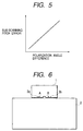
- buried heterojunction lasers show a luminous spot width smaller than conventional ones having a so-called planar structure so that the luminous spots of the buried heterojunction lasers of a semiconductor laser array are subjected to thermal stress in different directions in the vicinity thereof when the chip carrying the semiconductor lasers is soldered to a sub-mount. Then, in the case of a semiconductor laser array having a pair of luminous spots such as illustrated in Fig.
- the intervals of the sub-scanning pitch may vary depending on the resolution, they are 21 ⁇ m if the resolution is 1,200 dpi and 42 ⁇ m if the resolution is 600 dpi. Because of the highly accurate intervals of the sub-scanning pitch, an error up to several ⁇ m is not permissible. In other words, if the error due to the difference in the angle of polarization is 5 ⁇ m with a resolution of 1,200 dpi, the intervals may be 16 ⁇ m or 26 ⁇ m depending on the position along the mainscanning direction. Then, a so-called banding phenomenon (of varying pitch where a wide interval and a narrow interval appear alternately) arises to make it difficult to provide a high resolution image.
- an error of about 5 ⁇ m occurs in the sub-scanning pitch if the difference in the angle of polarization is about 20 degrees, although it may depend on the extent of double refraction of the scanning lens.
- the angle of polarization becomes variable as a function of the position of each luminous spot so that abnormal spot diameters and abnormal sub-scanning pitches are produced when laser beams pass through an optical part showing double refraction in an optical scanner.
- Another object of the present invention is to provide an optical scanner that can produce a high resolution image.
- Still another object of the present invention is to provide an optical scanner that can produce a high resolution image if a less costly plastic lens is used for it.
- a semiconductor laser array comprising:
- an optical scanner comprising:
- FIG. 1 is a schematic perspective view of an embodiment of semiconductor laser array according to the invention.
- FIGS. 2A and 2B are schematic illustrations of a plastic scanning lens that can be used for the purpose of the invention.
- FIG. 3 is a schematic cross sectional view of an optical scanner realized by using the semiconductor laser array of FIG. 1 as light source.
- FIG. 4 is a graph illustrating the relationship between the residual stress and the difference of angle of polarization at a luminous spot.
- FIG. 5 is a graph illustrating the relationship between the difference of angle of polarization and the error in the sub-scanning pitch.
- FIG. 6 is a schematic cross sectional view of a semiconductor laser array having a pair of luminous spots.
- FIG. 1 is a schematic perspective view of an embodiment of semiconductor laser array according to the invention.
- the sub-mount 2 of the embodiment is made of silicon that is available at low cost and a chip 1 is soldered to the sub-mount 2 in a junction down fashion from the viewpoint of heat emitting effect.
- the chip 1 comprises buried heterojunction type lasers having a reduced threshold current as disclosed in Japanese Patent Application Laid-Open No. 10-051078 in view of cross talk and drooping property.
- the chip 1 of this embodiment has two luminous spots 3a and 3b of semiconductor lasers.
- the temperature of the chip 1 and the sub-mount 2 rises to about 250 to 300°C and falls to room temperature after the completion of the soldering operation. If the chip 1 and the sub-mount 2 show a large difference in terms of thermal expansion, residual stress appears in the chip 1.
- Solder is fluidized at 300°C and hence the chip 1 and the sub-mount 2 show a difference of expansion of 0.04 ⁇ m at that temperature.
- the sub-mount 2 is cooled to ambient temperature before the expanded chip 1 restores its proper length at room temperature, residual stress appears near the luminous spots of the chip 1.
- the normal dimensions of the chip 1 is such that the resonator has a length between 200 ⁇ m and 300 ⁇ m, a width between 200 ⁇ m and 400 ⁇ m and a height between 50 ⁇ m and 150 ⁇ m.
- the sub-mount 2 normally has dimensions of about 0.6 to 0.9 mm ⁇ 0.8 to 1.2 mm x 0.3 to 0.5 mm. Obviously, the sub-mount 2 emits heat more easily to quickly lower its temperature and encourage the appearance of residual stress.
- FIG. 4 is a graph illustrating the relationship between the residual stress appearing near the luminous spots 3a and 3b and the difference of angle of polarization between them of the above embodiment.
- the difference of angle of polarization increases proportionally relative to the residual stress.
- the sub-scanning pitch of a semiconductor laser array showing such a difference of angle of polarization is regulated according to a predetermined resolution by means of the method as described in Japanese Patent Application Laid-Open No. 11-58828, the sub-scanning pitch is inevitably increased to give rise to an error in it to make it impossible to regulate it anymore because of a large difference of angle of polarization as seen from the graph of FIG. 5 illustrating the relationship between the difference of angle of polarization and the error in the sub-scanning pitch.
- a substantially collimated laser beam L is emitted from laser beam source 11 (semiconductor laser array) and deflected by an optical deflector 13 having a polygon mirror 12.
- Scanning lenses 10a and 10b are housed in an optical cabinet 14 in order to converge the deflected beam that is to be used for scanning to a spot having a predetermined contour.
- a sub-scanning pitch error can arise because of the use of the scanning lenses 10a and 10b provided to converge the beam to a spot having a predetermined contour at a predetermined location. Since the scanning lenses 10a and 10b are plastic lenses as described in Japanese Patent Application Laid-Open No. 10-048557 and show double refraction from the time of molding.
- FIGS. 2A and 2B are schematic illustrations of a plastic scanning lens 10.
- inclined lines 20a through 20d represent the direction of polarization and show that molecules in the lens 10 are oriented in such a way that the lens transmits the laser beam only along the direction of polarization due to the residual stress that arises when soldering the chip to the sub-mount.
- the beam 21 is scanned on the scanning lens 10 showing such double refraction (see FIG. 2B).
- the region indicated by X is a region that is practically free from double refraction whereas the regions Y1 and Y2 where a spot having a normal contour is formed are those showing double refraction.
- the beam 21 becomes to show an abnormal contour that is expanded vertically.
- the polarization characteristic attributable to the double refraction obtained at the write start side of the optical scanner and the one obtained at the write end side of the optical scanner are turned upside down to give rise to a sub-scanning pitch error.
- the difference of angle of polarization is large, it can give rise to not only a sub-scanning pitch error but also an abnormal contour for the spot.
- the residual stress appearing near the luminous spots 3a and 3b may be caused by the soldering.
- the chip 1 is soldered to the sub-mount while it is projecting from the corresponding end facet of the sub-mount 2 (by T in FIG. 1).
- the areas near the luminous spots 3a and 3b are substantially not influenced by the soldering to remarkably reduce the residual stress that appears after the soldering and hence the difference of angle of polarization between the two luminous spots 3a and 3b.
- the length of the chip 1, or the resonator length is between 200 ⁇ m and 300 ⁇ m, the above effect (of reducing the difference of angle of polarization) of the projecting part of the chip 1 becomes satisfactory when T is made equal to tens of several micrometers.
- the semiconductor laser array of the above described embodiment has two luminous spots on the chip 1, it may be needless to say that a similar effect can be obtained when a semiconductor laser array has three or more than three luminous spots. Additionally, while the above described optical scanner is provided with two scanning lenses 10, a similar effect can be obtained if it is provided with one, three or more than three lenses.
Landscapes
- Physics & Mathematics (AREA)
- Condensed Matter Physics & Semiconductors (AREA)
- General Physics & Mathematics (AREA)
- Electromagnetism (AREA)
- Optics & Photonics (AREA)
- Semiconductor Lasers (AREA)
- Mechanical Optical Scanning Systems (AREA)
- Laser Beam Printer (AREA)
- Facsimile Heads (AREA)
Abstract
Description
said plurality of luminous spots projecting toward the laser beam emitting side from the corresponding end facet of said mount.
Claims (7)
- A semiconductor laser array comprising:a chip having a plurality of luminous spots; anda mount for mounting said chip by means of solder;said plurality of luminous spots projecting toward the laser beam emitting side from the corresponding end facet of said mount.
- A semiconductor laser array according to claim 1, wherein
said mount is made of silicon. - A semiconductor laser array according to claim 1, wherein
the semiconductor lasers of said semiconductor laser array are buried heterojunction type lasers. - A semiconductor laser array according to claim 1, wherein
said chip is soldered to said mount in a fashion of junction down. - A semiconductor laser array according to claim 1, wherein
said plurality of luminous spots are driven independently. - An optical scanner comprising:a semiconductor laser array, said semiconductor laser array including a chip having a plurality of luminous spots and a mount for mounting said chip by means of solder;a rotary mirror for deflecting the laser beams emitted from said semiconductor laser array;a focussing lens for focussing the laser beams deflected by said rotary mirror on a surface to be scanned;said plurality of luminous spots projecting toward the laser beam emitting side from the corresponding end facet of said mount.
- An optical scanner according to claim 6, wherein
said lens is made of a plastic material.
Applications Claiming Priority (2)
| Application Number | Priority Date | Filing Date | Title |
|---|---|---|---|
| JP33844999 | 1999-11-29 | ||
| JP33844999A JP2001156379A (en) | 1999-11-29 | 1999-11-29 | Semiconductor laser array and optical scanning device |
Publications (3)
| Publication Number | Publication Date |
|---|---|
| EP1104061A2 true EP1104061A2 (en) | 2001-05-30 |
| EP1104061A3 EP1104061A3 (en) | 2002-11-13 |
| EP1104061B1 EP1104061B1 (en) | 2006-03-01 |
Family
ID=18318269
Family Applications (1)
| Application Number | Title | Priority Date | Filing Date |
|---|---|---|---|
| EP00126100A Expired - Lifetime EP1104061B1 (en) | 1999-11-29 | 2000-11-29 | Semiconductor laser array and optical scanner |
Country Status (4)
| Country | Link |
|---|---|
| US (1) | US6867796B1 (en) |
| EP (1) | EP1104061B1 (en) |
| JP (1) | JP2001156379A (en) |
| DE (1) | DE60026220T2 (en) |
Families Citing this family (3)
| Publication number | Priority date | Publication date | Assignee | Title |
|---|---|---|---|---|
| JP2006313875A (en) * | 2005-04-08 | 2006-11-16 | Mitsubishi Electric Corp | Semiconductor laser device |
| JP2009130206A (en) | 2007-11-26 | 2009-06-11 | Mitsubishi Electric Corp | Semiconductor light emitting device and manufacturing method thereof |
| US10297976B2 (en) * | 2015-05-19 | 2019-05-21 | Ii-Vi Laser Enterprise Gmbh | Low thermal resistance, stress-controlled diode laser assemblies |
Family Cites Families (12)
| Publication number | Priority date | Publication date | Assignee | Title |
|---|---|---|---|---|
| JPH067627B2 (en) | 1985-03-09 | 1994-01-26 | ソニー株式会社 | Method for manufacturing semiconductor laser device |
| JPH087288B2 (en) | 1986-11-20 | 1996-01-29 | 日本電信電話株式会社 | Method for manufacturing hybrid optical integrated circuit |
| JP2539878B2 (en) | 1988-02-12 | 1996-10-02 | 三菱電機株式会社 | Driving method for semiconductor laser device for laser printer |
| JP2780981B2 (en) | 1988-06-27 | 1998-07-30 | 三菱電機株式会社 | Multipoint emission type semiconductor laser and method of manufacturing the same |
| JPH0522530A (en) | 1991-07-17 | 1993-01-29 | Canon Inc | Laser light source device |
| JP3377553B2 (en) | 1993-05-13 | 2003-02-17 | 三菱電機株式会社 | Semiconductor laser device |
| JPH0918087A (en) | 1995-06-27 | 1997-01-17 | Nec Corp | Multi-beam semiconductor laser device |
| DE19601955C2 (en) | 1996-01-09 | 1997-12-11 | Siemens Ag | Optoelectronic transmitter module |
| JP3467151B2 (en) | 1996-05-23 | 2003-11-17 | 株式会社リコー | Optical module |
| JP3408070B2 (en) | 1996-07-30 | 2003-05-19 | キヤノン株式会社 | Scanning optical device |
| JPH1051078A (en) | 1996-08-06 | 1998-02-20 | Furukawa Electric Co Ltd:The | Semiconductor laser array and method of manufacturing the same |
| JPH1158828A (en) | 1997-08-14 | 1999-03-02 | Fuji Xerox Co Ltd | Laser array image forming apparatus |
-
1999
- 1999-11-29 JP JP33844999A patent/JP2001156379A/en active Pending
-
2000
- 2000-11-24 US US09/718,364 patent/US6867796B1/en not_active Expired - Fee Related
- 2000-11-29 EP EP00126100A patent/EP1104061B1/en not_active Expired - Lifetime
- 2000-11-29 DE DE60026220T patent/DE60026220T2/en not_active Expired - Lifetime
Also Published As
| Publication number | Publication date |
|---|---|
| DE60026220D1 (en) | 2006-04-27 |
| EP1104061B1 (en) | 2006-03-01 |
| DE60026220T2 (en) | 2006-11-16 |
| JP2001156379A (en) | 2001-06-08 |
| US6867796B1 (en) | 2005-03-15 |
| EP1104061A3 (en) | 2002-11-13 |
Similar Documents
| Publication | Publication Date | Title |
|---|---|---|
| EP0544002B1 (en) | Image-forming device | |
| US6798438B2 (en) | Image-recording device for a printing form, having an array of VCSEL light sources | |
| US4530574A (en) | Beam collimation and focusing of multi-emitter or broad emitter lasers | |
| US6606180B2 (en) | Light beam scanning device | |
| EP0100242B1 (en) | Optical system for a laser | |
| US5640188A (en) | Multiple diode laser employing mating substrates | |
| EP0844707A2 (en) | Multiple beam light source device and multiple beam scanning optical apparatus using the device | |
| US20050151828A1 (en) | Xerographic printing system with VCSEL-micro-optic laser printbar | |
| EP1104061B1 (en) | Semiconductor laser array and optical scanner | |
| US20040032483A1 (en) | Multi-beam laser scanning device | |
| US6740869B2 (en) | Light beam scanning device for micro-area light source | |
| JP2004066543A (en) | Semiconductor laser array light source | |
| US20040047377A1 (en) | Multilaser device for receiving a plurality of back beams by a common sensor | |
| KR100739761B1 (en) | Multi Beam Scanner | |
| JPH0470711A (en) | Laser scanning optical system | |
| US7265885B2 (en) | Multi-beam emitting device and light scanning unit employing the same | |
| JP2000330046A (en) | Optical scanning device | |
| US6804425B2 (en) | Optical Head | |
| JPH0899436A (en) | LED array head | |
| JPH0560994A (en) | Optical scanner | |
| KR100246445B1 (en) | Multi-beam laser scanner | |
| JPH11174353A (en) | Multi-beam scanning optical device | |
| JPH08304722A (en) | Multibeam scanning optical device | |
| JP3387805B2 (en) | Scanning optical system and image forming apparatus using the same | |
| JPH07110450A (en) | Optical scanning device |
Legal Events
| Date | Code | Title | Description |
|---|---|---|---|
| PUAI | Public reference made under article 153(3) epc to a published international application that has entered the european phase |
Free format text: ORIGINAL CODE: 0009012 |
|
| AK | Designated contracting states |
Kind code of ref document: A2 Designated state(s): AT BE CH CY DE DK ES FI FR GB GR IE IT LI LU MC NL PT SE TR |
|
| AX | Request for extension of the european patent |
Free format text: AL;LT;LV;MK;RO;SI |
|
| PUAL | Search report despatched |
Free format text: ORIGINAL CODE: 0009013 |
|
| AK | Designated contracting states |
Kind code of ref document: A3 Designated state(s): AT BE CH CY DE DK ES FI FR GB GR IE IT LI LU MC NL PT SE TR |
|
| AX | Request for extension of the european patent |
Free format text: AL;LT;LV;MK;RO;SI |
|
| 17P | Request for examination filed |
Effective date: 20030327 |
|
| 17Q | First examination report despatched |
Effective date: 20030430 |
|
| AKX | Designation fees paid |
Designated state(s): DE FR GB IT |
|
| GRAP | Despatch of communication of intention to grant a patent |
Free format text: ORIGINAL CODE: EPIDOSNIGR1 |
|
| GRAS | Grant fee paid |
Free format text: ORIGINAL CODE: EPIDOSNIGR3 |
|
| GRAA | (expected) grant |
Free format text: ORIGINAL CODE: 0009210 |
|
| AK | Designated contracting states |
Kind code of ref document: B1 Designated state(s): DE FR GB IT |
|
| PG25 | Lapsed in a contracting state [announced via postgrant information from national office to epo] |
Ref country code: IT Free format text: LAPSE BECAUSE OF FAILURE TO SUBMIT A TRANSLATION OF THE DESCRIPTION OR TO PAY THE FEE WITHIN THE PRESCRIBED TIME-LIMIT;WARNING: LAPSES OF ITALIAN PATENTS WITH EFFECTIVE DATE BEFORE 2007 MAY HAVE OCCURRED AT ANY TIME BEFORE 2007. THE CORRECT EFFECTIVE DATE MAY BE DIFFERENT FROM THE ONE RECORDED. Effective date: 20060301 |
|
| REG | Reference to a national code |
Ref country code: GB Ref legal event code: FG4D |
|
| REF | Corresponds to: |
Ref document number: 60026220 Country of ref document: DE Date of ref document: 20060427 Kind code of ref document: P |
|
| ET | Fr: translation filed | ||
| PLBE | No opposition filed within time limit |
Free format text: ORIGINAL CODE: 0009261 |
|
| STAA | Information on the status of an ep patent application or granted ep patent |
Free format text: STATUS: NO OPPOSITION FILED WITHIN TIME LIMIT |
|
| 26N | No opposition filed |
Effective date: 20061204 |
|
| PGFP | Annual fee paid to national office [announced via postgrant information from national office to epo] |
Ref country code: FR Payment date: 20131125 Year of fee payment: 14 |
|
| REG | Reference to a national code |
Ref country code: FR Ref legal event code: ST Effective date: 20150731 |
|
| PG25 | Lapsed in a contracting state [announced via postgrant information from national office to epo] |
Ref country code: FR Free format text: LAPSE BECAUSE OF NON-PAYMENT OF DUE FEES Effective date: 20141201 |
|
| PGFP | Annual fee paid to national office [announced via postgrant information from national office to epo] |
Ref country code: GB Payment date: 20151125 Year of fee payment: 16 Ref country code: DE Payment date: 20151130 Year of fee payment: 16 |
|
| REG | Reference to a national code |
Ref country code: DE Ref legal event code: R119 Ref document number: 60026220 Country of ref document: DE |
|
| GBPC | Gb: european patent ceased through non-payment of renewal fee |
Effective date: 20161129 |
|
| PG25 | Lapsed in a contracting state [announced via postgrant information from national office to epo] |
Ref country code: GB Free format text: LAPSE BECAUSE OF NON-PAYMENT OF DUE FEES Effective date: 20161129 Ref country code: DE Free format text: LAPSE BECAUSE OF NON-PAYMENT OF DUE FEES Effective date: 20170601 |