EP1104027A2 - Power semiconductor device having a ballast resistor region - Google Patents
Power semiconductor device having a ballast resistor region Download PDFInfo
- Publication number
- EP1104027A2 EP1104027A2 EP00121970A EP00121970A EP1104027A2 EP 1104027 A2 EP1104027 A2 EP 1104027A2 EP 00121970 A EP00121970 A EP 00121970A EP 00121970 A EP00121970 A EP 00121970A EP 1104027 A2 EP1104027 A2 EP 1104027A2
- Authority
- EP
- European Patent Office
- Prior art keywords
- substrate
- gate
- gate structures
- type
- partial
- Prior art date
- Legal status (The legal status is an assumption and is not a legal conclusion. Google has not performed a legal analysis and makes no representation as to the accuracy of the status listed.)
- Granted
Links
Images




Classifications
-
- H—ELECTRICITY
- H10—SEMICONDUCTOR DEVICES; ELECTRIC SOLID-STATE DEVICES NOT OTHERWISE PROVIDED FOR
- H10D—INORGANIC ELECTRIC SEMICONDUCTOR DEVICES
- H10D30/00—Field-effect transistors [FET]
- H10D30/01—Manufacture or treatment
- H10D30/021—Manufacture or treatment of FETs having insulated gates [IGFET]
- H10D30/028—Manufacture or treatment of FETs having insulated gates [IGFET] of double-diffused metal oxide semiconductor [DMOS] FETs
- H10D30/0291—Manufacture or treatment of FETs having insulated gates [IGFET] of double-diffused metal oxide semiconductor [DMOS] FETs of vertical DMOS [VDMOS] FETs
- H10D30/0293—Manufacture or treatment of FETs having insulated gates [IGFET] of double-diffused metal oxide semiconductor [DMOS] FETs of vertical DMOS [VDMOS] FETs using formation of insulating sidewall spacers
-
- H—ELECTRICITY
- H10—SEMICONDUCTOR DEVICES; ELECTRIC SOLID-STATE DEVICES NOT OTHERWISE PROVIDED FOR
- H10P—GENERIC PROCESSES OR APPARATUS FOR THE MANUFACTURE OR TREATMENT OF DEVICES COVERED BY CLASS H10
- H10P10/00—Bonding of wafers, substrates or parts of devices
-
- H—ELECTRICITY
- H10—SEMICONDUCTOR DEVICES; ELECTRIC SOLID-STATE DEVICES NOT OTHERWISE PROVIDED FOR
- H10D—INORGANIC ELECTRIC SEMICONDUCTOR DEVICES
- H10D12/00—Bipolar devices controlled by the field effect, e.g. insulated-gate bipolar transistors [IGBT]
- H10D12/01—Manufacture or treatment
- H10D12/031—Manufacture or treatment of IGBTs
- H10D12/032—Manufacture or treatment of IGBTs of vertical IGBTs
-
- H—ELECTRICITY
- H10—SEMICONDUCTOR DEVICES; ELECTRIC SOLID-STATE DEVICES NOT OTHERWISE PROVIDED FOR
- H10D—INORGANIC ELECTRIC SEMICONDUCTOR DEVICES
- H10D30/00—Field-effect transistors [FET]
- H10D30/01—Manufacture or treatment
- H10D30/021—Manufacture or treatment of FETs having insulated gates [IGFET]
- H10D30/028—Manufacture or treatment of FETs having insulated gates [IGFET] of double-diffused metal oxide semiconductor [DMOS] FETs
- H10D30/0291—Manufacture or treatment of FETs having insulated gates [IGFET] of double-diffused metal oxide semiconductor [DMOS] FETs of vertical DMOS [VDMOS] FETs
-
- H—ELECTRICITY
- H10—SEMICONDUCTOR DEVICES; ELECTRIC SOLID-STATE DEVICES NOT OTHERWISE PROVIDED FOR
- H10D—INORGANIC ELECTRIC SEMICONDUCTOR DEVICES
- H10D62/00—Semiconductor bodies, or regions thereof, of devices having potential barriers
- H10D62/10—Shapes, relative sizes or dispositions of the regions of the semiconductor bodies; Shapes of the semiconductor bodies
- H10D62/124—Shapes, relative sizes or dispositions of the regions of semiconductor bodies or of junctions between the regions
- H10D62/126—Top-view geometrical layouts of the regions or the junctions
- H10D62/127—Top-view geometrical layouts of the regions or the junctions of cellular field-effect devices, e.g. multicellular DMOS transistors or IGBTs
-
- H—ELECTRICITY
- H10—SEMICONDUCTOR DEVICES; ELECTRIC SOLID-STATE DEVICES NOT OTHERWISE PROVIDED FOR
- H10D—INORGANIC ELECTRIC SEMICONDUCTOR DEVICES
- H10D62/00—Semiconductor bodies, or regions thereof, of devices having potential barriers
- H10D62/10—Shapes, relative sizes or dispositions of the regions of the semiconductor bodies; Shapes of the semiconductor bodies
- H10D62/13—Semiconductor regions connected to electrodes carrying current to be rectified, amplified or switched, e.g. source or drain regions
- H10D62/141—Anode or cathode regions of thyristors; Collector or emitter regions of gated bipolar-mode devices, e.g. of IGBTs
- H10D62/142—Anode regions of thyristors or collector regions of gated bipolar-mode devices
-
- H—ELECTRICITY
- H10—SEMICONDUCTOR DEVICES; ELECTRIC SOLID-STATE DEVICES NOT OTHERWISE PROVIDED FOR
- H10D—INORGANIC ELECTRIC SEMICONDUCTOR DEVICES
- H10D84/00—Integrated devices formed in or on semiconductor substrates that comprise only semiconducting layers, e.g. on Si wafers or on GaAs-on-Si wafers
- H10D84/01—Manufacture or treatment
- H10D84/0102—Manufacture or treatment of thyristors having built-in components, e.g. thyristor having built-in diode
-
- H—ELECTRICITY
- H10—SEMICONDUCTOR DEVICES; ELECTRIC SOLID-STATE DEVICES NOT OTHERWISE PROVIDED FOR
- H10D—INORGANIC ELECTRIC SEMICONDUCTOR DEVICES
- H10D84/00—Integrated devices formed in or on semiconductor substrates that comprise only semiconducting layers, e.g. on Si wafers or on GaAs-on-Si wafers
- H10D84/101—Integrated devices comprising main components and built-in components, e.g. IGBT having built-in freewheel diode
- H10D84/141—VDMOS having built-in components
Definitions
- This invention relates to a power semiconductor device.
- insulated gate bipolar transistors improves immunity to latch-up and improves short circuit ruggedness. Others have thought that the improvement is due to an increase in the voltage drop in the P-region beneath the N+ source needed to activate a parasitic thyristor, and to de-biasing of the gate by the voltage drop in the ballast resistor.
- the ballast resistor is combined with the body effect of the device so that the voltage drop has negligible effect at operating current and adjusts the threshold voltage so that it increases by several volts under short circuit current conditions.
- the emitter is provided with an emitter ballast resistor and the body effect is modified by controlling the value of the emitter ballast resistor.
- the present invention provides a method for more precisely controlling the size and resistance of ballast resistors without the use of a masking layer.
- the invention provides a source/emitter ballast resistor that is self-aligned with a sidewall spacer of the cellular gate structures.
- the present invention includes a semiconductor device with an integral source/emitter ballast resistor comprising a semiconductor substrate, a P-well region in the substrate having a P-type polarity, a single gate with a plurality of partial first and second gate structures spaced apart from each other on the surface of the substrate, each partial gate structure having a gate sidewall spacer insulator along the opposite edges of the gate structures and said partial gate structures extending along opposite lengths of the P-well and covering opposite portions of said P-well, characterized in that a source or emitter region in the P-well region and having a pair of resistor regions of lightly doped N-type dopants, each resistor region extending along the length of the P-well and beneath the gate sidewall spacer insulator, and highly doped N-type contact regions in the substrate extending in a direction transverse to the edges of the partial gate structures for providing ohmic metal contact to the elongated emitter resistor regions.
- the invention provides a semiconductor device with an integral source/emitter ballast resistor.
- the device is fabricated in a semiconductor substrate, typically an N-type substrate.
- the substrate has an elongated P-well region where the edges of the P-well form PN junctions with the N-type substrate at the surface.
- a single gate has a plurality of partial gate structures that are spaced apart from each other on the surface of the substrate.
- Each gate structure has a gate oxide or a gate insulator layer on the substrate surface with a conductive gate on top of the gate insulator.
- Two opposing gate structures cover opposite elongated ends of a P-well region. On the edges of the gate structures facing each other, each gate structure has a sidewall spacer insulator.
- Beneath the sidewall spacer insulator is a self-aligned, lightly doped N-type region that forms the emitter/source ballast resistor. Extending transverse to the opposing elongated emitter ballast resistors are one or more heavily doped N-type contact regions. The remaining surface of the substrate is doped with a P+ type dopant in order to eliminate the effect of the lightly doped N-type region, except for the region beneath the sidewall spacer insulators.
- the threshold voltage of devices made with the invention increase by a negligible amount, i.e., a few millivolts.
- the emitter ballast resistors have a dramatic effect upon limiting the short circuit current.
- the body effect due to the emitter ballast resistor produces a threshold voltage that is anywhere from 2-4 volts greater than the normal threshold voltage. As such, a device under short circuit conditions will saturate sooner and therefore will be protected against carrying excess current.
- the present invention includes a method for forming a semiconductor device with an integral source/emitter ballast resistor comprising, on a semiconductor substrate forming first and second partial gate structures spaced apart from each other on the surface of the substrate, each having a gate insulator layer on the surface of the semiconductor substrate and a conductive gate material on the gate insulator, characterized by implanting the surface of the semiconductor with P-type ions, diffusing the P-type ions into the substrate to form a P-type well, masking the substrate to expose regions extending from one partial gate structure to the other, implanting the exposed regions with a heavy dose of N-type ions, on each edge of the partial gate structures, forming a sidewall spacer insulator extending along opposite lengths of the P-well, implanting the region between the partial gate structures with a heavy dose of P-type ions to compensate for the light N-type doping in the exposed portion of the substrate and to form elongated resistor regions of lightly doped N-type dopants, each resistor region extending along
- the process also includes the method for fabricating the structure.
- the elongated P-well is formed in the surface of the semiconductor with an N-type doping.
- the gate structure is formed on the surface of the semiconductor substrate.
- the P-well dopant is implanted into the surface of the substrate without need for a further mask.
- an N-type dopant is implanted into the surface of the semiconductor.
- the N-type dopant is then diffused down into the semiconductor but remains substantially aligned with the edges of the gate structure.
- the gate is modified to add a sidewall spacer. Sidewall spacing is a conventional step in gate fabrication.
- the substrate is masked to establish N+ contact regions.
- This mask is a non-critical mask since the N-type contact regions will self-align with the emitter ballast resistors. Thereafter, the mask is stripped and the surface is again implanted with a P-type dopant in order to eliminate the effect of the lightly doped N-region.
- the surface of the semiconductor provides alternate regions of P+ and N+. The N+ regions extend across the face of the semiconductor from one sidewall to the next. The edges of the N+ regions are connected to the emitter ballast resistors that extend along the length of the P-well beneath the sidewall spacers.
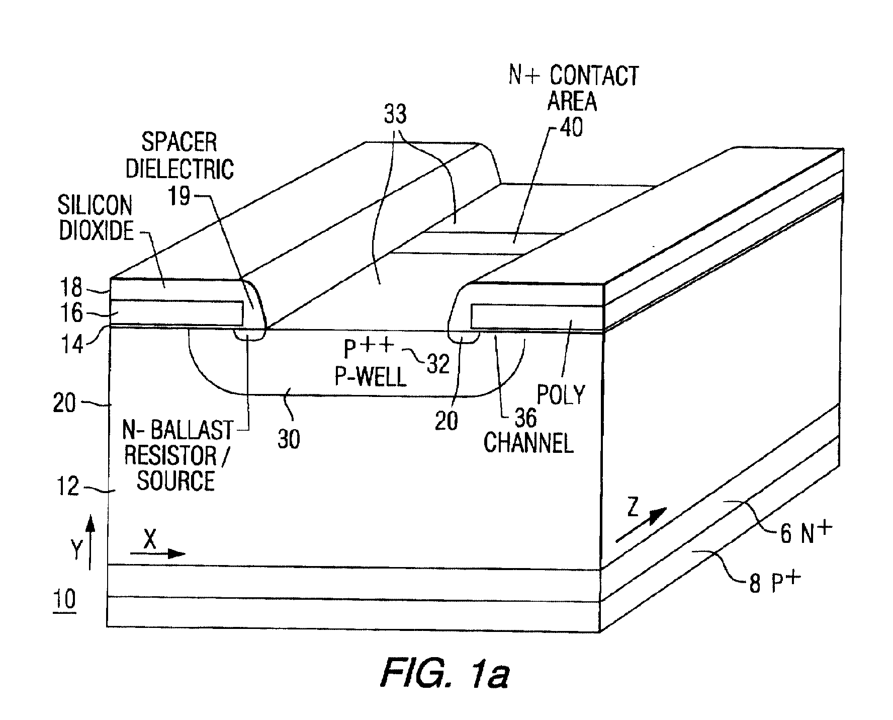
- Figure 1 is a partial perspective of a semiconductor substrate with self-aligned ballast emitter source resistors.
- Figure 1b is a planar view of the structure shown in Figure 1a.
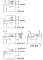
- Figure 2 is a series of process steps showing formation of the structure of Figure 1.
- Figure 3 is an alternate set of fabrication steps creating the structure shown in Figure 1.
- Figure 4 is a set of graphs showing selected parameters as a function of channel doping.
- Figure 5 is a sketch of cell used to simulate the emitter ballast resistor.
- Figure 6 shows comparative shifts in Vth.
- Figure 7 shows comparative shifts as a function of Vgs.
- Figure 8 shows comparative values for peak current for different emitter ballast resistances.
- Figure 9 shows comparative voltage drops for different emitter ballast resistances.
- Figure 10 shows comparative collector currents as a function of time for different emitter ballast resistances.
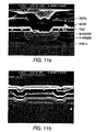
- Figures 11a and 11b are scanning electron photomicrographs of cross sections of finished devices having emitter ballast resistances.
- Figure 12 shows comparative graphs of changes in threshold voltage for different emitter ballast resistances.
- FIG. 1a, 1b there are shown partial sections of a device including the invention. The following description will be given for an IGBT.
- FIG 10 shows a typical IGBT device that includes the inventive source/ emitter ballast resistor 20.
- the device includes an N-type substrate 12 with a highly P-doped anode layer 8 on the bottom covered by a highly n-doped drain layer 6.
- P-well 30 is in the bulk of the wafer near the top surface thereof.
- the surface of the P-well 30 has a highly doped P-type layer 32.
- the P-well 30 extends along the length of the device in the z direction, i.e., into the paper. The z direction is better shown in Figure 1b.
- portions of the gate are opposite each other.
- the gate portions include a gate oxide layer 14 on the surface of the substrate.
- the gate 16 includes a number of parallel gate fingers 16a, 16b...16n.
- the fingers are conventionally connected to each other to form a single gate.
- the gate portions are elongated fingers; in the cellular version the gate portions are on the opposite boundaries of the cell.
- Covering the doped polysilicon 16 is a silicon dioxide layer 18 that includes sidewall spacers 19.
- Sidewall spacers 19 also run the z length of the P-wells 30.
- Beneath the sidewall spacers 19 are elongated ballast resistors 20. These resistors are tied together by N+ contact areas 40 that extend from one ballast resistor across the surface of the semiconductor to the other ballast resistor.
- the emitter region of the device includes a plurality of N+ contact regions that extend generally in the x direction across the surface of the substrate 12.
- the ballast resistors extend in the z direction on opposite sides of the P-well structure 30
- FIG 2 there are shown a series of steps for fabricating the structure shown in Figure 1.
- the following description and the drawings omit the drain layer 6 and the anode layer 8. However, those layers are part of a typical IGBT and MCT.
- a MOSFET or a DMOS device would include only the additional heavily doped N-layer 6.
- the substrate 12 is covered with a gate oxide 14.
- the oxide may be deposited or thermally grown, and preferably is thermally grown.
- a layer of polysilicon is then deposited on the gate oxide followed by deposition of another oxide layer 18 for protecting the polysilicon layer 16.
- the substrate is patterned to define the gate type structures.
- the gate oxide, polysilicon 16 and oxide 18 are removed from regions that define an underlying P-well.
- a P-well implant is made with a suitable dopant, such as boron. Boron is a rapidly-diffusing dopant and quickly diffuses to form the P-well 30 that extends beneath the gate structure.
- a light dose of an N-type dopant 20 is implanted into the surface of substrate 12.
- Implant 20 is a slower diffusing dopant such as arsenic or antimony. When it diffuses, its edge remains substantially aligned with the edge of the gate structure.
- an oxide layer is deposited over the substrate. The deposited layer merges with the original oxide layer 18 to form a thick oxide 18.1 over the polysilicon 16. The thick oxide layer 18.1 is then vertically etched (an isotropically etched) to expose a portion of the surface of the substrate and to provide a spacer oxide 19 covering the polysilicon 16.
- a layer of photoresist 42 is deposited over the surface of the substrate 12 and is patterned to expose the N+ contact region as shown in Figure 1b.
- An N-type implant 40 with a heavy concentration is implanted into the surface of the substrate in order to form the N+ contact area 40.
- the photoresist is then stripped and a heavily-doped P-type implant is made into the surface to form the P+ regions 33.
- the P-type implant counteracts the lightly-doped N-type region 20 in all areas except beneath the sidewall spacer 19.
- the P+ implant has no effect upon the N+ contact areas 40.
- Figure 2d corresponds to the right hand portion of Figure 1a.
- FIG. 3 An alternate approach and method allows fabrication without applying a top level oxide layer 18.
- This approach is shown in Figure 3.
- polysilicon layer 16 is deposited with an oxide and then is etched vertically to leave the remaining oxide spacer 18.3.
- substrate 12 is patterned with photoresist 42 to expose contact regions for an N-type implant to form the N+ contact regions 40.
- the photoresist 42 is stripped and a thin low-temperature oxide layer 60 is grown over the entire surface.
- the P+ implant 32 is made into the surface of the substrate 12.
- a thin oxide layer 60 is grown and etched in a conventional fashion to provide a mask that covers the contact area.
- a BPSG layer is put down and etched in a conventional fashion using a mask that requires alignment to the polysilicon 16.
- the thin undoped oxide layer 60 prevents counter-doping of the contacts by the phosphorous in the BPSG layer 70.
- the thin undoped oxide 60 may also be deposited before the contact step to reduce damage from the P-type implant 32.
- the invention provides to form emitter/source ballast resistors that are in series and effectively part of the emitter or source contact.
- the resistors are formed with a geometry that would generally be impossible to achieve using traditional photomasking operations.
- the cross-section of the resistor is defined by the width of the gate sidewall spacer.
- the resulting resistor only alters the normal operating conditions of the device by changing the threshold voltage a few millivolts.
- the resistor has an impact on the body effect of the device.
- increased current flowing through the ballast resistors causes a voltage drop of 0.2-0.4v which in turn increases the Vtl by 2-4 volts due to the enhanced body effect.
- channel conductance goes down and therefore the current is reduced.
- saturation occurs at a much lower current, thereby allowing the device to withstand a short circuit for a longer time.
- the invention has little or no effect on devices during normal operation, but has a dramatic effect upon the device when the device enters a dangerous, short circuit condition.
- ⁇ PNP is the gain of the IGBT
- V gs is the applied gate-source voltage
- V th is the threshold voltage
- ⁇ m is the effective channel mobility
- C ox is the oxide capacitance per unit area given by ⁇ ox / ⁇ ox
- W chi is the channel width
- L ch is the channel length
- R ball is the magnitude of the ballast resistance.
- the source-body junction is reverse biased by the drop V sb in the ballast resistance as given by equation (6). If the body effect parameter is small, the change in V th , is small, and the reduction in peak short-circuit current comes largely from de-biasing the gate by the drop in the ballast resistance - as previously thought. lf, however, the body effect parameter is sufficiently large, even a small drop V sb can result in a significant increase in V th, leading to a dramatic reduction in peak short-circuit current.
- V th a large body effectinduced change in V th may be obtained under overcurrent conditions if the body effect parameter is made large, and a drop of 0.5V or so is obtained across the ballast resistance.
- the body effect parameter increases with the V th voltage, since it is controlled by the same factors.
- the increase in V th for a given bias V sb is almost independent of oxide thickness for devices with the same initial V th0 .
- the body effect in emitter ballasted IGBTs is examined in more detail by numerically simulating the structure.
- Figure 7 shows that for a given value of V th0 , the body effect is greater for a 700A thick gate oxide vs. a 1500A thick oxide.
- FIG 11 shows a scanning electron microscope picture of a finished device using the process of Figure 2.
- the device had an active area of 0.4cm 2 , a blocking voltage rating of 600V, and was formed as a stripe with a 4 ⁇ m Poly opening and 16 ⁇ m Poly web.
- the small contact pattern was formed in a self-aligned fashion, allowing the use of projection aligners and a 4 ⁇ m minimum photo design rule. This allows the designer to maximize the injection enhancement effect [3] without the need for steppers and tight photo tolerances.
- the N+ pattern consisted of 4pm stripes running perpendicular to the Poly at 16 ⁇ m intervals.
- a power semiconductor device has an integral source/emitter ballast resistor.
- the gate has partial gate structures spaced apart from each other. Emitter resistors are provided beneath sidewall spacers on the ends of the gate structures. The emitter resistors have little effect on the threshold voltage under normal operating conditions, but rapidly saturate the device during short circuit conditions.
Landscapes
- Thyristors (AREA)
- Metal-Oxide And Bipolar Metal-Oxide Semiconductor Integrated Circuits (AREA)
- Semiconductor Integrated Circuits (AREA)
- Bipolar Transistors (AREA)
Abstract
Description
- The light doping of the source region allows a much higher value of resistance over a given length of the cell in the z direction to be realized that would be possible with prior art N+ sources.
- Since the width of the resistor is set by the spacer, a much smaller width, and therefore, a much higher resistance may be realized than with lithographically defined resistors. The spacer width may be accurately controlled by control of the deposited thickness of the spacer material, the RIE spacer etch and the sidewall angle of the Polysilicon.
- Controlling the length of the resistor in the z-direction limits the non-uniformity of current flow during short-circuit.
- A high threshold and high body effect parameter is used in conjunction with this ballast resistance to maximize the reduction in peak current flow through the IGBT during short-circuit fault conditions. It will be shown how a 50-100mV drop in the ballast resistor at operating currents (100A/cm2) are sufficient to produce a 2-4V change in effective threshold voltage under high current conditions with proper body effect engineering. This allows the production of devices with over 10µs short circuit withstand time (SCWT) with virtually no degradation in conduction-drop, The fact that the effective threshold voltage now increases with device current means that this robustness can now be achieved without resorting to a high low current threshold voltage, which causes higher conduction and turn-on losses when the gate drive voltage is 15V.


Figure 11 shows a scanning electron microscope picture of a finished device using the process of Figure 2. The device had an active area of 0.4cm2, a blocking voltage rating of 600V, and was formed as a stripe with a 4 µm Poly opening and 16 µm Poly web. The small contact pattern was formed in a self-aligned fashion, allowing the use of projection aligners and a 4 µm minimum photo design rule. This allows the designer to maximize the injection enhancement effect [3] without the need for steppers and tight photo tolerances. The N+ pattern consisted of 4pm stripes running perpendicular to the Poly at 16 µm intervals.
| Parameter | Self-Aligned device A | Self-Aligned device B |
| VCESAT (27C) | 1.6 V | 1.53 V |
| VCESAT (150C) | 1.57 V | 1.495 V |
| EOFF (150C, 40A, 480V) | 1.485 mJ | 1.75 mJ |
| Latching | CL 210 A | CL 160 A |
| VTH | 6.52 V | 7.33 V |
| Turn-on dI/dt | 960 A/µs | 800 A/µs |
| Turn-on dV/st | 18.2 V/ns | 17 V/ns |
| EON (150C, 40A, 480V) | 1.71 mJ | 1.97 mJ |
| SCMT IPK (A) | 320 A | 280 A |
| SCWT (360V, 125C, Rg=3 Ω) | 16 µs | 17 µs |
- The change in threshold voltage versus the drop in the ballast resistor Vsb is shown in Figure 12. It becomes clear that the change in Vth is not linear with Vsb (eqtn. 2), and that the percent decrease in peak short circuit current will be greater for the first 0.5V drop in the ballast resistance than for the next 0.5V. Therefore, designing for a drop of greater than 0.5V at peak short-circuit currents is not optimal.
- For a given low current threshold voltage Vth0, the increase in Vth with Vsb is greater for higher initial values of Vth0. This is because with higher channel dopings, the body effect parameter is greater. However, as the value of Vth is increased, the turn-on speed of the IGBT can be slowed to an undesirable extent especially when the gate drive voltage drops from 15V to 12V. In order to prevent excessive turn-on losses in the IGBT, a value of Vth0 in the range of 5V to 7V is practical.
- As shown through numerical simulations, the body effect in power devices with nonuniformly doped channels is somewhat different than for devices with uniformly doped channels. In particular, the effect of oxide thickness on the body effect parameter is greater. A given drop in the ballast resistor Vsb produces a greater Vth, shift for a thinner gate oxide. However, the peak current through the device increases inversely with oxide thickness as shown in equation (1). These two competing effects must be considered in design. In a design where these effects cancel each other, for the same VCE(SAT)-EOFF performance, the device with the thicker gate oxide has a lower input and gate-drain capacitance. This benefit is countered by the lower P-well doping, that leads to a higher -resistance under the source region, and makes the device more prone to latch-up. It also lowers the peak lattice temperature at which the threshold voltage goes to zero, leading to loss of gate control and device destruction. Since the device is very robust against latch-up, the oxide thickness can be effectively increased from 500-700A to 1000-1500A without a excessive compromise in SCWT, latch-up and UIS capability.
- In order to obtain a lower Vth along with a high body effect parameter, it is necessary to reduce the Vth without lowering the doping in the channel. This may be achieved only by changing the flatband voltage, which in turn requires that the gate-semiconductor workfunction difference be altered. In particular, the use of a gate material with a lower workfunction (e.g. Magnesium, Cesium) will allow a low Vth n-channel device with a high body effect parameter.
- A further technique for maximizing the effect of the ballast resistor and increasing the Vth at high currents would be to form a non-linear ballast resistance. If the ballast resistance value increases as the current through it increases, the effect is to minimize the degradation in VCE(SAT) at rated current, but to still get a large drop Vsb under overcurrent conditions, providing good short-circuit robustness. This requires the formation of a lightly doped - resistor in the P-well, which gets increasingly depleted as the drop Vsb increases. A lightly doped resistance must be formed in this process by counter-doping the P-well region. In order to control this resistance accurately, this is more easily done if the P-well doping is low to begin with, and if the - implanted layer is diffused to form a flatter doping profile. This tends to favor the use of light P-well doping and thicker gate oxides, within the constraints of latch-up immunity.
Claims (9)
- A semiconductor device with an integral source/emitter ballast resistor comprising a semiconductor substrate, a P-well region in the substrate having a P-type polarity, a single gate with a plurality of partial first and second gate structures spaced apart from each other on the surface of the substrate, each partial gate structure having a gate sidewall spacer insulator along the opposite edges of the gate structures and said partial gate structures extending along opposite lengths of the P-well and covering opposite portions of said P-well, characterized in that a source or emitter region in the P-well region and having a pair of resistor regions of lightly doped N-type dopants, each resistor region extending along the length of the P-well and beneath the gate sidewall spacer insulator, and highly doped N-type contact regions in the substrate extending in a direction transverse to the edges of the partial gate structures for providing ohmic metal contact to the elongated emitter resistor regions.
- A semiconductor device as claimed in claim 1 characterized in that regions of the substrate between the gate sidewall spacer insulators and between heavily doped N-type regions is heavily doped with P-type dopants, and in which N-type dopants are substituted for P-type dopants and vice versa, including one of group consisting of MOSFET, IGBT, MCT and DMOS devices.
- A semiconductor device as claimed in claim 1 characterized in that the partial gate structures are either stripes or cells, and the resistors alter the normal threshold voltage by a few millivolts and alter the short circuit threshold voltage by more than 10%.
- A semiconductor device with an integral source/emitter ballast resistor comprising a semiconductor substrate, a P-well region in the substrate having a P-type polarity, a single gate with a plurality of partial first and second gate structures spaced apart from each other on the surface of the substrate, each partial gate structure having a gate sidewall spacer insulator along the opposite edges of the gate structures and said partial gate structures extending along opposite lengths of the P-well and covering opposite portions of said P-well, characterized in that a highly doped N-type source or emitter region in the substrate and extending transverse to the gate structures, means in the substrate aligned with the partial gate structures and connected to the source/emitter regions for generating a first threshold voltage during normal operation of the device and for generating a second threshold voltage during a short circuit operation of the device in order to rapidly saturate the device during short circuit in the event of a short circuit.
- A device as claimed in claim 4 characterized in that the means in the substrate generates a first threshold voltage increase of several millivolts during normal operation of the device and a second threshold voltage increase of several volts during short circuit operation of the device, and the means in the substrate alters the conductance of channel beneath the gate in response to short circuit current through the device in order to reduce the current through the device, and the means in the substrate includes means for altering the body effect.
- A device as claimed in claim 5 characterized in that the means in the substrate comprises lightly doped N-type regions self aligned with the edges of the cellular gate structures, the lightly doped N-type regions are self aligned with the sidewall insulator of the partial gate structures, and the partial gate structures are either stripes or cells.
- A semiconductor device with an integral source/emitter ballast resistor comprising, a semiconductor substrate, a P-well region in the substrate having a P-type polarity, a single gate with a plurality of partial first and second gate structures spaced apart from each other on the surface of the substrate, each partial gate structure having a gate sidewall spacer insulator along the opposite edges of the gate structures and said partial gate structures extending along opposite lengths of the P-well and covering opposite portions of said P-well, characterized in that a highly doped N-type source or emitter region in the substrate and extending transverse to the gate structures, means in the substrate, aligned with the partial gate structures, connected to the source/emitter regions, and responsive to a short circuit condition in the device for reducing the current carried by the device when the device is short circuited.
- A method for forming a semiconductor device with an integral source/emitter ballast resistor comprising, on a semiconductor substrate forming first and second partial gate structures spaced apart from each other on the surface of the substrate, each having a gate insulator layer on the surface of the semiconductor substrate and a conductive gate material on the gate insulator, characterized by implanting the surface of the semiconductor with P-type ions, diffusing the P-type ions into the substrate to form a P-type well, masking the substrate to expose regions extending from one partial gate structure to the other, implanting the exposed regions with a heavy dose of N-type ions, on each edge of the partial gate structures, forming a sidewall spacer insulator extending along opposite lengths of the P-well, implanting the region between the partial gate structures with a heavy dose of P-type ions to compensate for the light N-type doping in the exposed portion of the substrate and to form elongated resistor regions of lightly doped N-type dopants, each resistor region extending along the length of the P-well and beneath the gate sidewall spacer insulator and said resistors connected to each other by the highly doped N-type regions in the substrate that extend in a direction transverse to the edges of the partial gate structures.
- A method as claimed in claim 8 characterized by the further step of diffusing the light N-type dopant immediately after implant in order to lower the threshold voltage of the device, and in which the resistors alter the normal operational threshold by several millivolts and alter the short circuit threshold by one or more volts.
Applications Claiming Priority (2)
| Application Number | Priority Date | Filing Date | Title |
|---|---|---|---|
| US450872 | 1999-11-29 | ||
| US09/450,872 US6437419B1 (en) | 1999-11-29 | 1999-11-29 | Emitter ballast resistor with enhanced body effect to improve the short circuit withstand capability of power devices |
Publications (3)
| Publication Number | Publication Date |
|---|---|
| EP1104027A2 true EP1104027A2 (en) | 2001-05-30 |
| EP1104027A3 EP1104027A3 (en) | 2004-02-18 |
| EP1104027B1 EP1104027B1 (en) | 2011-01-19 |
Family
ID=23789857
Family Applications (1)
| Application Number | Title | Priority Date | Filing Date |
|---|---|---|---|
| EP00121970A Expired - Lifetime EP1104027B1 (en) | 1999-11-29 | 2000-10-09 | Power semiconductor device having a ballast resistor region |
Country Status (5)
| Country | Link |
|---|---|
| US (1) | US6437419B1 (en) |
| EP (1) | EP1104027B1 (en) |
| JP (1) | JP2001189455A (en) |
| KR (1) | KR100749979B1 (en) |
| DE (1) | DE60045542D1 (en) |
Cited By (2)
| Publication number | Priority date | Publication date | Assignee | Title |
|---|---|---|---|---|
| CN110120422A (en) * | 2018-02-07 | 2019-08-13 | 万国半导体(开曼)股份有限公司 | Source electrode ballast for P- channel groove MOSFET |
| EP3975261A1 (en) * | 2020-09-29 | 2022-03-30 | Infineon Technologies Dresden GmbH & Co . KG | Voltage-controlled switching device with resistive path |
Families Citing this family (17)
| Publication number | Priority date | Publication date | Assignee | Title |
|---|---|---|---|---|
| US6798019B2 (en) * | 2002-01-18 | 2004-09-28 | Fairchild Semiconductor Corporation | IGBT with channel resistors |
| US6864537B1 (en) | 2003-01-03 | 2005-03-08 | Micrel, Incorporated | Thick gate oxide transistor and electrostatic discharge protection utilizing thick gate oxide transistors |
| US6861711B2 (en) | 2003-01-03 | 2005-03-01 | Micrel, Incorporated | Thick gate oxide transistor and electrostatic discharge protection utilizing thick gate oxide transistors |
| US6888710B2 (en) | 2003-01-03 | 2005-05-03 | Micrel, Incorporated | Insulated gate bipolar transistor and electrostatic discharge cell protection utilizing insulated gate bipolar transistors |
| US7087973B2 (en) * | 2003-04-01 | 2006-08-08 | Micrel, Incorporated | Ballast resistors for transistor devices |
| JP5040240B2 (en) * | 2006-09-29 | 2012-10-03 | 三菱電機株式会社 | Insulated gate semiconductor device |
| US8304829B2 (en) | 2008-12-08 | 2012-11-06 | Fairchild Semiconductor Corporation | Trench-based power semiconductor devices with increased breakdown voltage characteristics |
| US8174067B2 (en) | 2008-12-08 | 2012-05-08 | Fairchild Semiconductor Corporation | Trench-based power semiconductor devices with increased breakdown voltage characteristics |
| US8227855B2 (en) | 2009-02-09 | 2012-07-24 | Fairchild Semiconductor Corporation | Semiconductor devices with stable and controlled avalanche characteristics and methods of fabricating the same |
| US8148749B2 (en) | 2009-02-19 | 2012-04-03 | Fairchild Semiconductor Corporation | Trench-shielded semiconductor device |
| US8049276B2 (en) | 2009-06-12 | 2011-11-01 | Fairchild Semiconductor Corporation | Reduced process sensitivity of electrode-semiconductor rectifiers |
| US8863064B1 (en) * | 2012-03-23 | 2014-10-14 | Suvolta, Inc. | SRAM cell layout structure and devices therefrom |
| KR101416881B1 (en) * | 2013-11-13 | 2014-07-08 | 에이피반도체 주식회사 | Power BJT with base ballast resistor |
| US9899512B2 (en) | 2016-02-24 | 2018-02-20 | General Electric Company | Silicon carbide device and method of making thereof |
| EP4099392A1 (en) | 2021-06-03 | 2022-12-07 | NXP USA, Inc. | Termination ballast resistor in power mosfets with trench field plate |
| JP2025043984A (en) * | 2023-09-19 | 2025-04-01 | 株式会社東芝 | Semiconductor Device |
| CN119421474B (en) * | 2025-01-08 | 2025-03-14 | 深圳云潼微电子科技有限公司 | Built-in ballast resistor of IGBT device and forming method thereof and IGBT device |
Family Cites Families (17)
| Publication number | Priority date | Publication date | Assignee | Title |
|---|---|---|---|---|
| US3936863A (en) * | 1974-09-09 | 1976-02-03 | Rca Corporation | Integrated power transistor with ballasting resistance and breakdown protection |
| JP2700025B2 (en) * | 1985-12-24 | 1998-01-19 | 富士電機株式会社 | Bipolar vertical MOSFET |
| US4860072A (en) * | 1986-03-05 | 1989-08-22 | Ixys Corporation | Monolithic semiconductor device and method of manufacturing same |
| JPS6384164A (en) * | 1986-09-29 | 1988-04-14 | Nissan Motor Co Ltd | Perpendicular mosfet |
| US5298785A (en) * | 1987-05-15 | 1994-03-29 | Fuji Electric Co., Ltd. | Semiconductor device |
| US5206182A (en) | 1989-06-08 | 1993-04-27 | United Technologies Corporation | Trench isolation process |
| JP3210657B2 (en) * | 1989-11-27 | 2001-09-17 | 株式会社日立製作所 | Heterojunction bipolar transistor |
| JP2536302B2 (en) * | 1990-04-30 | 1996-09-18 | 日本電装株式会社 | Insulated gate type bipolar transistor |
| JPH04196174A (en) * | 1990-11-26 | 1992-07-15 | Fuji Electric Co Ltd | Insulated-gate bipolar |
| IT1252102B (en) * | 1991-11-26 | 1995-06-02 | Cons Ric Microelettronica | VERTICAL STRUCTURE MONOLITHIC SEMICONDUCTOR DEVICE WITH DEEP BASE POWER TRANSISTOR AND FINGER EMITTER WITH BALLAST RESISTANCE |
| US5736755A (en) * | 1992-11-09 | 1998-04-07 | Delco Electronics Corporation | Vertical PNP power device with different ballastic resistant vertical PNP transistors |
| US5374844A (en) * | 1993-03-25 | 1994-12-20 | Micrel, Inc. | Bipolar transistor structure using ballast resistor |
| JPH08279561A (en) * | 1995-04-07 | 1996-10-22 | Mitsubishi Electric Corp | Bipolar transistor and amplifier and integrated circuit using the bipolar transistor |
| US5637902A (en) | 1996-01-16 | 1997-06-10 | Vlsi Technology, Inc. | N-well resistor as a ballast resistor for output MOSFET |
| JP3209091B2 (en) * | 1996-05-30 | 2001-09-17 | 富士電機株式会社 | Semiconductor device having insulated gate bipolar transistor |
| JPH10335345A (en) * | 1997-06-04 | 1998-12-18 | Mitsubishi Electric Corp | Heterojunction bipolar transistor and manufacturing method thereof |
| JP3594482B2 (en) * | 1998-04-02 | 2004-12-02 | 三菱電機株式会社 | Heterojunction bipolar transistor |
-
1999
- 1999-11-29 US US09/450,872 patent/US6437419B1/en not_active Expired - Lifetime
-
2000
- 2000-10-09 DE DE60045542T patent/DE60045542D1/en not_active Expired - Lifetime
- 2000-10-09 EP EP00121970A patent/EP1104027B1/en not_active Expired - Lifetime
- 2000-11-28 KR KR1020000071297A patent/KR100749979B1/en not_active Expired - Lifetime
- 2000-11-28 JP JP2000360784A patent/JP2001189455A/en not_active Ceased
Cited By (6)
| Publication number | Priority date | Publication date | Assignee | Title |
|---|---|---|---|---|
| CN110120422A (en) * | 2018-02-07 | 2019-08-13 | 万国半导体(开曼)股份有限公司 | Source electrode ballast for P- channel groove MOSFET |
| CN110120422B (en) * | 2018-02-07 | 2022-07-01 | 万国半导体(开曼)股份有限公司 | Source Ballast for P-Channel Trench MOSFETs |
| EP3975261A1 (en) * | 2020-09-29 | 2022-03-30 | Infineon Technologies Dresden GmbH & Co . KG | Voltage-controlled switching device with resistive path |
| KR20220043891A (en) * | 2020-09-29 | 2022-04-05 | 인피니언 테크놀로지스 드레스덴 게엠베하 운트 콤파니 카게 | Voltage-controlled switching device with resistive path |
| CN114334491A (en) * | 2020-09-29 | 2022-04-12 | 英飞凌科技德累斯顿公司 | Voltage-controlled switch device and switch assembly |
| US12266680B2 (en) | 2020-09-29 | 2025-04-01 | Infineon Technologies Dresden GmbH & Co. KG | Voltage-controlled switching device with resistive path |
Also Published As
| Publication number | Publication date |
|---|---|
| DE60045542D1 (en) | 2011-03-03 |
| US6437419B1 (en) | 2002-08-20 |
| KR100749979B1 (en) | 2007-08-16 |
| EP1104027B1 (en) | 2011-01-19 |
| EP1104027A3 (en) | 2004-02-18 |
| KR20010051995A (en) | 2001-06-25 |
| JP2001189455A (en) | 2001-07-10 |
Similar Documents
| Publication | Publication Date | Title |
|---|---|---|
| EP1104027B1 (en) | Power semiconductor device having a ballast resistor region | |
| US5105243A (en) | Conductivity-modulation metal oxide field effect transistor with single gate structure | |
| US5985721A (en) | Single feature size MOS technology power device | |
| USRE38953E1 (en) | Insulated gate semiconductor device and method of manufacturing the same | |
| US7687336B2 (en) | Method of manufacturing a MOSFET structure | |
| EP0696054A1 (en) | Process for the manufacturing of high-density MOS-technology power devices | |
| US5528063A (en) | Conductive-overlaid self-aligned MOS-gated semiconductor devices | |
| US5382536A (en) | Method of fabricating lateral DMOS structure | |
| US6054737A (en) | High density MOS technology power device | |
| US20090283796A1 (en) | Semiconductor device and method for forming the same | |
| KR20000029577A (en) | Semiconductor component with linear current-to-voltage characteristics | |
| EP0689238A1 (en) | MOS-technology power device manufacturing process | |
| KR100701712B1 (en) | Horizontal Thin Film SIO Device | |
| US5237186A (en) | Conductivity-modulation metal oxide field effect transistor with single gate structure | |
| KR0165909B1 (en) | Gate insulated semiconductor device and manufacturing method thereof | |
| US6147382A (en) | Semiconductor switching device with segmented sources | |
| US6780722B2 (en) | Field effect transistor on insulating layer and manufacturing method | |
| KR100197539B1 (en) | Semiconductor device and method of manufacturing the same | |
| US20230163167A1 (en) | Semiconductor device including a trench gate structure | |
| KR100206193B1 (en) | Power semiconductor device and manufacturing method thereof | |
| US5184201A (en) | Static induction transistor | |
| JPH0878670A (en) | Charge injection type insulated gate semiconductor device |
Legal Events
| Date | Code | Title | Description |
|---|---|---|---|
| PUAI | Public reference made under article 153(3) epc to a published international application that has entered the european phase |
Free format text: ORIGINAL CODE: 0009012 |
|
| AK | Designated contracting states |
Kind code of ref document: A2 Designated state(s): AT BE CH CY DE DK ES FI FR GB GR IE IT LI LU MC NL PT SE |
|
| AX | Request for extension of the european patent |
Free format text: AL;LT;LV;MK;RO;SI |
|
| PUAL | Search report despatched |
Free format text: ORIGINAL CODE: 0009013 |
|
| AK | Designated contracting states |
Kind code of ref document: A3 Designated state(s): AT BE CH CY DE DK ES FI FR GB GR IE IT LI LU MC NL PT SE |
|
| AX | Request for extension of the european patent |
Extension state: AL LT LV MK RO SI |
|
| 17P | Request for examination filed |
Effective date: 20040616 |
|
| AKX | Designation fees paid |
Designated state(s): DE FR GB IT SE |
|
| 17Q | First examination report despatched |
Effective date: 20061211 |
|
| GRAP | Despatch of communication of intention to grant a patent |
Free format text: ORIGINAL CODE: EPIDOSNIGR1 |
|
| RAP1 | Party data changed (applicant data changed or rights of an application transferred) |
Owner name: FAIRCHILD SEMICONDUCTOR CORPORATION |
|
| GRAS | Grant fee paid |
Free format text: ORIGINAL CODE: EPIDOSNIGR3 |
|
| GRAA | (expected) grant |
Free format text: ORIGINAL CODE: 0009210 |
|
| AK | Designated contracting states |
Kind code of ref document: B1 Designated state(s): DE FR GB IT SE |
|
| REG | Reference to a national code |
Ref country code: GB Ref legal event code: FG4D |
|
| REF | Corresponds to: |
Ref document number: 60045542 Country of ref document: DE Date of ref document: 20110303 Kind code of ref document: P |
|
| REG | Reference to a national code |
Ref country code: DE Ref legal event code: R096 Ref document number: 60045542 Country of ref document: DE Effective date: 20110303 |
|
| PG25 | Lapsed in a contracting state [announced via postgrant information from national office to epo] |
Ref country code: SE Free format text: LAPSE BECAUSE OF FAILURE TO SUBMIT A TRANSLATION OF THE DESCRIPTION OR TO PAY THE FEE WITHIN THE PRESCRIBED TIME-LIMIT Effective date: 20110119 |
|
| PLBE | No opposition filed within time limit |
Free format text: ORIGINAL CODE: 0009261 |
|
| STAA | Information on the status of an ep patent application or granted ep patent |
Free format text: STATUS: NO OPPOSITION FILED WITHIN TIME LIMIT |
|
| 26N | No opposition filed |
Effective date: 20111020 |
|
| PG25 | Lapsed in a contracting state [announced via postgrant information from national office to epo] |
Ref country code: IT Free format text: LAPSE BECAUSE OF FAILURE TO SUBMIT A TRANSLATION OF THE DESCRIPTION OR TO PAY THE FEE WITHIN THE PRESCRIBED TIME-LIMIT Effective date: 20110119 |
|
| REG | Reference to a national code |
Ref country code: DE Ref legal event code: R097 Ref document number: 60045542 Country of ref document: DE Effective date: 20111020 |
|
| GBPC | Gb: european patent ceased through non-payment of renewal fee |
Effective date: 20111009 |
|
| REG | Reference to a national code |
Ref country code: FR Ref legal event code: ST Effective date: 20120629 |
|
| PG25 | Lapsed in a contracting state [announced via postgrant information from national office to epo] |
Ref country code: GB Free format text: LAPSE BECAUSE OF NON-PAYMENT OF DUE FEES Effective date: 20111009 Ref country code: FR Free format text: LAPSE BECAUSE OF NON-PAYMENT OF DUE FEES Effective date: 20111102 |
|
| PGFP | Annual fee paid to national office [announced via postgrant information from national office to epo] |
Ref country code: DE Payment date: 20190918 Year of fee payment: 20 |
|
| REG | Reference to a national code |
Ref country code: DE Ref legal event code: R071 Ref document number: 60045542 Country of ref document: DE |