EP1103995A1 - Electronic component, and electronic apparatus in which the electronic component is mounted and its manufacturing method - Google Patents
Electronic component, and electronic apparatus in which the electronic component is mounted and its manufacturing method Download PDFInfo
- Publication number
- EP1103995A1 EP1103995A1 EP00937171A EP00937171A EP1103995A1 EP 1103995 A1 EP1103995 A1 EP 1103995A1 EP 00937171 A EP00937171 A EP 00937171A EP 00937171 A EP00937171 A EP 00937171A EP 1103995 A1 EP1103995 A1 EP 1103995A1
- Authority
- EP
- European Patent Office
- Prior art keywords
- electronic component
- external terminal
- alloy
- electronic
- alloy layer
- Prior art date
- Legal status (The legal status is an assumption and is not a legal conclusion. Google has not performed a legal analysis and makes no representation as to the accuracy of the status listed.)
- Withdrawn
Links
Images
Classifications
-
- H—ELECTRICITY
- H01—ELECTRIC ELEMENTS
- H01C—RESISTORS
- H01C1/00—Details
- H01C1/14—Terminals or tapping points specially adapted for resistors; Arrangements of terminals or tapping points on resistors
-
- H—ELECTRICITY
- H05—ELECTRIC TECHNIQUES NOT OTHERWISE PROVIDED FOR
- H05K—PRINTED CIRCUITS; CASINGS OR CONSTRUCTIONAL DETAILS OF ELECTRIC APPARATUS; MANUFACTURE OF ASSEMBLAGES OF ELECTRICAL COMPONENTS
- H05K3/00—Apparatus or processes for manufacturing printed circuits
- H05K3/30—Assembling printed circuits with electric components, e.g. with resistors
- H05K3/32—Assembling printed circuits with electric components, e.g. with resistors electrically connecting electric components or wires to printed circuits
-
- B—PERFORMING OPERATIONS; TRANSPORTING
- B23—MACHINE TOOLS; METAL-WORKING NOT OTHERWISE PROVIDED FOR
- B23K—SOLDERING OR UNSOLDERING; WELDING; CLADDING OR PLATING BY SOLDERING OR WELDING; CUTTING BY APPLYING HEAT LOCALLY, e.g. FLAME CUTTING; WORKING BY LASER BEAM
- B23K35/00—Rods, electrodes, materials, or media, for use in soldering, welding, or cutting
- B23K35/22—Rods, electrodes, materials, or media, for use in soldering, welding, or cutting characterised by the composition or nature of the material
- B23K35/24—Selection of soldering or welding materials proper
- B23K35/26—Selection of soldering or welding materials proper with the principal constituent melting at less than 400°C
- B23K35/262—Sn as the principal constituent
-
- H—ELECTRICITY
- H01—ELECTRIC ELEMENTS
- H01C—RESISTORS
- H01C17/00—Apparatus or processes specially adapted for manufacturing resistors
- H01C17/28—Apparatus or processes specially adapted for manufacturing resistors adapted for applying terminals
-
- H—ELECTRICITY
- H01—ELECTRIC ELEMENTS
- H01F—MAGNETS; INDUCTANCES; TRANSFORMERS; SELECTION OF MATERIALS FOR THEIR MAGNETIC PROPERTIES
- H01F27/00—Details of transformers or inductances, in general
- H01F27/28—Coils; Windings; Conductive connections
- H01F27/29—Terminals; Tapping arrangements for signal inductances
- H01F27/292—Surface mounted devices
-
- H—ELECTRICITY
- H05—ELECTRIC TECHNIQUES NOT OTHERWISE PROVIDED FOR
- H05K—PRINTED CIRCUITS; CASINGS OR CONSTRUCTIONAL DETAILS OF ELECTRIC APPARATUS; MANUFACTURE OF ASSEMBLAGES OF ELECTRICAL COMPONENTS
- H05K3/00—Apparatus or processes for manufacturing printed circuits
- H05K3/30—Assembling printed circuits with electric components, e.g. with resistors
- H05K3/32—Assembling printed circuits with electric components, e.g. with resistors electrically connecting electric components or wires to printed circuits
- H05K3/34—Assembling printed circuits with electric components, e.g. with resistors electrically connecting electric components or wires to printed circuits by soldering
- H05K3/346—Solder materials or compositions specially adapted therefor
-
- H—ELECTRICITY
- H01—ELECTRIC ELEMENTS
- H01F—MAGNETS; INDUCTANCES; TRANSFORMERS; SELECTION OF MATERIALS FOR THEIR MAGNETIC PROPERTIES
- H01F27/00—Details of transformers or inductances, in general
- H01F27/28—Coils; Windings; Conductive connections
- H01F27/29—Terminals; Tapping arrangements for signal inductances
- H01F2027/297—Terminals; Tapping arrangements for signal inductances with pin-like terminal to be inserted in hole of printed path
Definitions
- the present invention relates to an electronic component, an electronic apparatus mounted the electronic component and a method of manufacturing the electronic apparatus.
- the invention relates particularly to the electronic component, the electronic apparatus mounted the electronic component and the method for manufacturing the apparatus to address problems of the environment on the earth.
- an Sn-Bi, Sn-Ag, Sn-Zn or Sn-Cu based-lead-free solder is actively in research and development instead of a conventional Sn-Pb based eutectic solder widely-used in assembly of the electronic apparatuses.
- the Sn-Cu based-eutectic ally is especially noted as a solder used in a flow-infiltration soldering apparatus.
- the Sn-Cu based-eutectic alloy can improve mechanical and electrical characteristics properties in a solder joint as well as economical situation.
- an external terminal in the electronic component placed on a printed circuit board is Sn-Pb plated or Sn plated in the surface of the terminal.
- An electronic component plated with Sn-Bi or Sn-Ag is considered to produce a lead-free external terminal.
- whiskers may be formed depending on a usage condition, and furthermore, a circuit may short.
- the present invention can address the problems and provide the electronic component which is friendly to the environment of the earth and highly-reliable in a joint between the external terminal of the electronic component and the circuit pattern on the printed circuit board.
- Sn-Cu alloy layer is disposed over the surface of an external terminal in an electronic component.
- the Sn-Cu alloy layer contains 0.5-3% of copper.
- An electronic apparatus of the present invention employs the electronic component of the present invention.
- the electronic component is coupled to an circuit pattern with a Sn-Cu eutectic alloy.
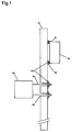
- Fig 1 is a cross sectional view of the electronic apparatus according to the embodiment of the present invention.
- circuit pattern 2 made of a copper foil etched with a desired pattern is formed over printed circuit board 1 having a paper phenol substrate, a glass epoxy substrate or the like as a base material.
- Printed circuit board 1 includes through-hole 5 where wire 4 is inserted.
- Wire 4 is an external terminal of first electronic component 3 such as a resistor, a capacitor or a inductor.
- Wire 4 includes a metal wire made of iron or copper over which a Sn-Cu alloy layer and a plating metal layer made of nickel or copper are formed.
- the Sn-Cu alloy layer is formed over the metal wire via the plating metal layer.
- These surface alloy layers can be formed with various methods.
- plating method has advantages in the device assembly and cost. Plating can control easily the composition of the alloy of the surface layer.
- the Sn-Cu alloy in the outermost layer of wire 4 and external terminal 7 contains 0.5-3% of Cu.
- Table 1 shows a relation among a rate of forming whiskers, solder-affinity, and a Cu concentration in the Sn-Cu alloy.
- the rate of forming whiskers is determined as following. Wire 4 plated with Sn-Cu alloy is folded 180 degree and left at 60°C in an atmosphere of 95% RH for 1000 hours, and then, a surface at a folded portion is observed. The "x" shows that an Sn needle-like protrusion longer than 50 ⁇ m is observed. The circle denotes the other situation.
- Solder-affinity is determined by measuring a zero-crossing time when Sn-Cu alloy-plated wire 4 and the second electronic component are left at 60°C in an atmosphere of 95% RH for 168 hours and then immersed in a soldering bath with dissolved Sn-Cu alloy.
- the "x" shows that the zero crossing time is not less than 3 seconds, and the circle shows the other result.
- Cu-Concentration in Alloy (%) 0 0.3 0.5 1.0 3.0 5.0 Rate of Forming Whiskers 5/10 3/10 0/10 0/10 0/10 0/10 Solder-affinity ⁇ ⁇ ⁇ ⁇ X
- the outermost layer of wire 4 or external terminal 7 in the second electronic component is made of Sn-Cu alloy and the Sn-Cu alloy contains 0.5-3% of Cu, whiskers are not formed, and solder-affinity is favorable.
- wire 4 of first electronic component 3 and external terminal 7 of second component 6 are electrically coupled to circuit pattern 2 on printed circuit board 1 respectively via Sn-Cu eutectic alloy layer.
- wire 4 or external terminal 7 is immersed in the melted Sn-Cu eutectic alloy.
- circuit pattern 2 made by etching a copper foil into desired pattern is formed over printed circuit board 1 having through-hole 5.
- wire 4 having the Sn-Cu alloy layer in first electronic component 3 is inserted into through-hole 5, and second electronic component 6 having external terminal 7 with Sn-Cu alloy layer is fixed by an adhesive if necessary,
- wire 4 of first electronic component 3 and external terminal 7 of second electronic component 6 are electrically jointed to circuit pattern 2 on printed circuit board 1 with the flow-infiltration method using molted lead-free Sn-Cu eutectic alloy. They are jointed by Sn-Cu eutectic alloy layer 8. Because wire 4 of first electronic component 3 and external terminal 7 of second electronic component 6 are coated with Sn-Cu alloy layer of the embodiment, different metals do not exist between Sn-Cu eutectic alloy layer 8 for joint and wire 4 or external terminal 7. The connection between the electronic component and circuit pattern is thus stable.
- the method of manufacturing the electronic apparatus by using the flow-infiltration method for soldering is described. Furthermore, when mounted electronic components are all surface-mounted type and also the surface of the external terminal thereof is coated with Sn-CU alloy layer with a composition of the alloy of the present invention, the flow soldering using Sn-Cu alloy can be used.
- Sn-Cu eutectic alloy is used, however, when manufacturing the electronic apparatuses, Sn-Cu alloys of no-eutectic type also can be used depending on conditions.
- the electronic component of the present invention includes a Sn-Cu alloy layer having a specified Cu-concentration over the surface of an external terminal. Therefore, when the external terminal and a circuit pattern on a printed circuit board are jointed with a flow-infiltration method using a molted Sn-Cu alloy, different metals do not solve out into the Sn-Cu alloy. Consequently, because different metal do not exist in the jointed portion, a stable joint is provided, and reliability of the electronic apparatus is improved.
- the electronic apparatus of the present invention which has a Sn-Cu alloy layer with the most favorable Cu-concentration over the surface of its external terminal, is also reliable for preservation.
Landscapes
- Engineering & Computer Science (AREA)
- Microelectronics & Electronic Packaging (AREA)
- Manufacturing & Machinery (AREA)
- Power Engineering (AREA)
- Mechanical Engineering (AREA)
- Electric Connection Of Electric Components To Printed Circuits (AREA)
- Manufacturing Of Printed Wiring (AREA)
- Lead Frames For Integrated Circuits (AREA)
- Non-Insulated Conductors (AREA)
Abstract
An electronic component, which is friendly to the environment of the
earth and has high reliability in a joint between an external terminal in the
electronic component and a circuit pattern on a printed circuit board, is
provided. Further, an electronic apparatus on which the electronic
component is mounted and a manufacturing method of the electronic
apparatus are provided. The electronic component of the present invention has
a wire having a Sn-Cu alloy layer as the outermost layer or the external
terminal with the Sn-Cu alloy layer as the outermost layer. In the
manufacturing method, the electronic component is electrically coupled to a
desired circuit pattern on the printed circuit board by the Sn-Cu alloy layer.
Description
The present invention relates to an electronic component, an electronic
apparatus mounted the electronic component and a method of manufacturing
the electronic apparatus. The invention relates particularly to the electronic
component, the electronic apparatus mounted the electronic component and
the method for manufacturing the apparatus to address problems of the
environment on the earth.
Recently, for improving the pollution of the environment on the earth, a
big effort has been actively made for not using hazardous substance such as
lead in electronic apparatuses such as television receivers or video tape
recorders.
Under this situation, an Sn-Bi, Sn-Ag, Sn-Zn or Sn-Cu based-lead-free
solder is actively in research and development instead of a conventional Sn-Pb
based eutectic solder widely-used in assembly of the electronic apparatuses.
In these lead free solders, the Sn-Cu based-eutectic ally is especially noted as a
solder used in a flow-infiltration soldering apparatus. The Sn-Cu based-eutectic
alloy can improve mechanical and electrical characteristics properties
in a solder joint as well as economical situation.
On the other hand, in the soldering by a flow-infiltration method using
the Sn-Cu based-eutectic alloy, an external terminal in the electronic
component placed on a printed circuit board is Sn-Pb plated or Sn plated in
the surface of the terminal. An electronic component plated with Sn-Bi or
Sn-Ag is considered to produce a lead-free external terminal.
When different metal such as Pb, Bi, Ag, or Zn is mixed into the melted
Sn-Cu eutectic alloy and the mixture is left for a long time, a circuit pattern on
the printed circuit board is peel off a Sn-Cu alloy layer. Accordingly,
reliability of the apparatus lowered. The peeling is called "lift-off'.
In the electronic component of which external terminal is plated with
Sn containing no other metals, whiskers may be formed depending on a usage
condition, and furthermore, a circuit may short.
The present invention can address the problems and provide the
electronic component which is friendly to the environment of the earth and
highly-reliable in a joint between the external terminal of the electronic
component and the circuit pattern on the printed circuit board.
In the present invention, Sn-Cu alloy layer is disposed over the surface
of an external terminal in an electronic component. The Sn-Cu alloy layer
contains 0.5-3% of copper. An electronic apparatus of the present invention
employs the electronic component of the present invention. The electronic
component is coupled to an circuit pattern with a Sn-Cu eutectic alloy.
An electronic apparatus in the embodiment of the present invention will
be described with referring to a drawing hereinafter.
Fig 1 is a cross sectional view of the electronic apparatus according to
the embodiment of the present invention.
In Fig. 1, circuit pattern 2 made of a copper foil etched with a desired
pattern is formed over printed circuit board 1 having a paper phenol substrate,
a glass epoxy substrate or the like as a base material. Printed circuit board 1
includes through-hole 5 where wire 4 is inserted. Wire 4 is an external
terminal of first electronic component 3 such as a resistor, a capacitor or a
inductor.
Wire 4 includes a metal wire made of iron or copper over which a Sn-Cu
alloy layer and a plating metal layer made of nickel or copper are formed.
The Sn-Cu alloy layer is formed over the metal wire via the plating metal
layer. External terminal 7 of wire-less and surface-mount-type second
electronic component 6, such as a resistor, a capacitor or a inductor, includes
the Sn-Cu alloy layer as an outermost layer over the surface of sintered silver
and glass via a barrier metal layer made of nickel or the like.
These surface alloy layers can be formed with various methods. In
general, plating method has advantages in the device assembly and cost.
Plating can control easily the composition of the alloy of the surface layer.
In the embodiment, the Sn-Cu alloy in the outermost layer of wire 4 and
external terminal 7 contains 0.5-3% of Cu.
Table 1 shows a relation among a rate of forming whiskers, solder-affinity,
and a Cu concentration in the Sn-Cu alloy. The rate of forming
whiskers is determined as following. Wire 4 plated with Sn-Cu alloy is folded
180 degree and left at 60°C in an atmosphere of 95% RH for 1000 hours, and
then, a surface at a folded portion is observed. The "x" shows that an Sn
needle-like protrusion longer than 50µm is observed. The circle denotes the
other situation.
Solder-affinity is determined by measuring a zero-crossing time when
Sn-Cu alloy-plated wire 4 and the second electronic component are left at 60°C
in an atmosphere of 95% RH for 168 hours and then immersed in a soldering
bath with dissolved Sn-Cu alloy. The "x" shows that the zero crossing time is
not less than 3 seconds, and the circle shows the other result.
| Cu-Concentration in Alloy (%) | 0 | 0.3 | 0.5 | 1.0 | 3.0 | 5.0 |
| Rate of Forming Whiskers | 5/10 | 3/10 | 0/10 | 0/10 | 0/10 | 0/10 |
| Solder-affinity | ○ | ○ | ○ | ○ | ○ | X |
As evident from table 1, in the case that the outermost layer of wire 4 or
external terminal 7 in the second electronic component is made of Sn-Cu alloy
and the Sn-Cu alloy contains 0.5-3% of Cu, whiskers are not formed, and
solder-affinity is favorable.
Moreover, wire 4 of first electronic component 3 and external terminal 7
of second component 6 are electrically coupled to circuit pattern 2 on printed
circuit board 1 respectively via Sn-Cu eutectic alloy layer. When soldering,
wire 4 or external terminal 7 is immersed in the melted Sn-Cu eutectic alloy.
A manufacturing method of the electronic apparatus as shown above
will be described.
First, circuit pattern 2 made by etching a copper foil into desired pattern
is formed over printed circuit board 1 having through-hole 5.
Then, wire 4 having the Sn-Cu alloy layer in first electronic component
3 is inserted into through-hole 5, and second electronic component 6 having
external terminal 7 with Sn-Cu alloy layer is fixed by an adhesive if necessary,
Then, wire 4 of first electronic component 3 and external terminal 7 of
second electronic component 6 are electrically jointed to circuit pattern 2 on
printed circuit board 1 with the flow-infiltration method using molted lead-free
Sn-Cu eutectic alloy. They are jointed by Sn-Cu eutectic alloy layer 8.
Because wire 4 of first electronic component 3 and external terminal 7 of
second electronic component 6 are coated with Sn-Cu alloy layer of the
embodiment, different metals do not exist between Sn-Cu eutectic alloy layer 8
for joint and wire 4 or external terminal 7. The connection between the
electronic component and circuit pattern is thus stable.
In the above description, the method of manufacturing the electronic
apparatus by using the flow-infiltration method for soldering is described.
Furthermore, when mounted electronic components are all surface-mounted
type and also the surface of the external terminal thereof is coated with Sn-CU
alloy layer with a composition of the alloy of the present invention, the flow
soldering using Sn-Cu alloy can be used.
And also, in the above description, Sn-Cu eutectic alloy is used, however,
when manufacturing the electronic apparatuses, Sn-Cu alloys of no-eutectic
type also can be used depending on conditions.
As shown above, the electronic component of the present invention
includes a Sn-Cu alloy layer having a specified Cu-concentration over the
surface of an external terminal. Therefore, when the external terminal and a
circuit pattern on a printed circuit board are jointed with a flow-infiltration
method using a molted Sn-Cu alloy, different metals do not solve out into the
Sn-Cu alloy. Consequently, because different metal do not exist in the jointed
portion, a stable joint is provided, and reliability of the electronic apparatus is
improved. The electronic apparatus of the present invention, which has a
Sn-Cu alloy layer with the most favorable Cu-concentration over the surface of
its external terminal, is also reliable for preservation.
According to the present invention, without using metal affecting the
environment of the earth such as lead, highly-reliable electronic apparatus
can be produced with great industrial availability.
Claims (8)
- An electronic component comprising:an external terminal; andan Sn-Cu alloy layer over a surface of said external terminal
- The electronic component according to claim 1, wherein said Sn-Cu alloy layer contains 0.5-3% of Cu.
- An electronic apparatus comprising:wherein said external terminal of said electronic component and a circuit pattern on said printed circuit board are electrically jointed with Sn-Cu based alloy containing no lead.a printed circuit board; andan electronic component comprising:an external terminal; andan Sn-Cu alloy layer over a surface of said external terminal,
- The electronic apparatus according to claim 3, wherein said Sn-Cu alloy layer over the surface of said external terminal contains 0.5-3% of Cu.
- The electronic apparatus according to claim 3, wherein said Sn-Cu base alloy jointing said external terminal of said electronic component and the circuit pattern on said printed circuit board is Sn-Cu eutectic alloy.
- A manufacturing method of manufacturing an electronic apparatus comprising the steps of:forming an Sn-Cu alloy layer over a surface of an external terminal of an electronic component;mounting the electronic component on a printed circuit board; andelectrically jointing the external terminal of the electronic component and a circuit pattern on the printed circuit board with Sn-Cu based alloy containing no lead.
- The manufacturing method according to claim 6, wherein the Sn-Cu alloy layer over the surface of the external terminal contains 0.5-3% of Cu.
- The manufacturing method according to claim 6, wherein the Sn-Cu based alloy jointing the external terminal of the electronic component and the circuit pattern on the printed circuit board is Sn-Cu eutectic alloy.
Applications Claiming Priority (3)
| Application Number | Priority Date | Filing Date | Title |
|---|---|---|---|
| JP11161904A JP2000349217A (en) | 1999-06-09 | 1999-06-09 | Electronic component, electronic device mounting this electronic component, and method of manufacturing the same |
| JP16190499 | 1999-06-09 | ||
| PCT/JP2000/003682 WO2000075940A1 (en) | 1999-06-09 | 2000-06-07 | Electronic component, and electronic apparatus in which the electronic component is mounted and its manufacturing method |
Publications (2)
| Publication Number | Publication Date |
|---|---|
| EP1103995A1 true EP1103995A1 (en) | 2001-05-30 |
| EP1103995A4 EP1103995A4 (en) | 2004-08-11 |
Family
ID=15744240
Family Applications (1)
| Application Number | Title | Priority Date | Filing Date |
|---|---|---|---|
| EP00937171A Withdrawn EP1103995A4 (en) | 1999-06-09 | 2000-06-07 | ELECTRONIC COMPONENT, APPARATUS IN WHICH THIS COMPONENT IS MOUNTED AND METHOD FOR MANUFACTURING THE APPARATUS |
Country Status (7)
| Country | Link |
|---|---|
| EP (1) | EP1103995A4 (en) |
| JP (1) | JP2000349217A (en) |
| KR (1) | KR100404563B1 (en) |
| CN (1) | CN1259678C (en) |
| ID (1) | ID27853A (en) |
| TW (1) | TW541549B (en) |
| WO (1) | WO2000075940A1 (en) |
Cited By (1)
| Publication number | Priority date | Publication date | Assignee | Title |
|---|---|---|---|---|
| EP4401098A1 (en) * | 2023-01-13 | 2024-07-17 | Huawei Digital Power Technologies Co., Ltd. | Magnetic device and manufacturing method thereof, and electronic device |
Families Citing this family (6)
| Publication number | Priority date | Publication date | Assignee | Title |
|---|---|---|---|---|
| US6603678B2 (en) | 2001-01-11 | 2003-08-05 | Hewlett-Packard Development Company, L.P. | Thermally-assisted switching of magnetic memory elements |
| US7397074B2 (en) | 2005-01-12 | 2008-07-08 | Samsung Electronics Co., Ltd. | RF field heated diodes for providing thermally assisted switching to magnetic memory elements |
| US20130168146A1 (en) * | 2011-12-28 | 2013-07-04 | Jin-San Kim | Metal terminal block adapted for surface mounting and method of mounting the same |
| CN103366923A (en) * | 2012-04-01 | 2013-10-23 | 厦门天迈节能照明有限公司 | Location short pin magnetic ring insertion piece |
| US9642276B2 (en) * | 2014-12-01 | 2017-05-02 | Tesla, Inc. | Welding and soldering of transistor leads |
| CN104540334A (en) * | 2014-12-20 | 2015-04-22 | 东莞立德精密工业有限公司 | SMT process assembly method of plug-in capacitor |
Family Cites Families (7)
| Publication number | Priority date | Publication date | Assignee | Title |
|---|---|---|---|---|
| GB721881A (en) * | 1950-09-29 | 1955-01-12 | Gunther Laubmeyer | Improvements in methods of soldering and solder therefor |
| JPS61196564A (en) * | 1985-02-25 | 1986-08-30 | シーメンス、アクチエンゲゼルシヤフト | Film carrier integrated circuit and manufacture thereof |
| JPH0745666A (en) * | 1993-08-03 | 1995-02-14 | Fujitsu Ltd | Electronic component mounting method |
| DE69530990T2 (en) * | 1994-09-27 | 2004-05-19 | Seiko Epson Corp. | CIRCUIT BOARD, METHOD FOR THEIR PRODUCTION AND ELECTRONIC DEVICES |
| DE19512838C2 (en) * | 1995-04-06 | 2000-09-14 | Hella Kg Hueck & Co | Electrical or electronic device |
| JPH10214706A (en) * | 1997-01-29 | 1998-08-11 | Mitsubishi Materials Corp | Chip type thermistor |
| JPH10286688A (en) * | 1997-04-15 | 1998-10-27 | Murata Mfg Co Ltd | Soldering goods |
-
1999
- 1999-06-09 JP JP11161904A patent/JP2000349217A/en active Pending
-
2000
- 2000-06-07 EP EP00937171A patent/EP1103995A4/en not_active Withdrawn
- 2000-06-07 KR KR10-2001-7001743A patent/KR100404563B1/en not_active Expired - Fee Related
- 2000-06-07 WO PCT/JP2000/003682 patent/WO2000075940A1/en not_active Ceased
- 2000-06-07 ID IDW20010324A patent/ID27853A/en unknown
- 2000-06-07 CN CNB008010633A patent/CN1259678C/en not_active Expired - Fee Related
- 2000-06-08 TW TW089111151A patent/TW541549B/en active
Cited By (1)
| Publication number | Priority date | Publication date | Assignee | Title |
|---|---|---|---|---|
| EP4401098A1 (en) * | 2023-01-13 | 2024-07-17 | Huawei Digital Power Technologies Co., Ltd. | Magnetic device and manufacturing method thereof, and electronic device |
Also Published As
| Publication number | Publication date |
|---|---|
| JP2000349217A (en) | 2000-12-15 |
| EP1103995A4 (en) | 2004-08-11 |
| TW541549B (en) | 2003-07-11 |
| KR20010072384A (en) | 2001-07-31 |
| KR100404563B1 (en) | 2003-11-05 |
| CN1313993A (en) | 2001-09-19 |
| ID27853A (en) | 2001-04-26 |
| WO2000075940A1 (en) | 2000-12-14 |
| CN1259678C (en) | 2006-06-14 |
Similar Documents
| Publication | Publication Date | Title |
|---|---|---|
| JPH10303518A (en) | Electronic component mounting substrate, electronic component mounting substrate, and method of joining tin / zinc alloy | |
| US6264093B1 (en) | Lead-free solder process for printed wiring boards | |
| GB2383552A (en) | Use of a barrier layer on a Cu substrate when using a Sn-Bi alloy as solder | |
| WO1998036626A1 (en) | Printed circuit assembly | |
| US20030178476A1 (en) | Solder paste, electronic -component assembly and soldering method | |
| JP2002224880A (en) | Solder paste and electronic equipment | |
| EP1103995A1 (en) | Electronic component, and electronic apparatus in which the electronic component is mounted and its manufacturing method | |
| JP2003332731A (en) | ARTICLE SOLDERED WITH Pb-FREE SOLDER | |
| EP1557235A1 (en) | Lead-free solder and soldered article | |
| TW590836B (en) | Method of mounting electronic parts with Sn-Zn solder free of Pb without reduction in bonding strength | |
| JP2000054189A (en) | Electric / electronic component material used by bonding Sn-Bi solder, electric / electronic component using the same, electric / electronic component mounting board, and solder bonding or mounting method using the same | |
| JP2003112285A (en) | Solder paste | |
| KR20050035083A (en) | Pb-free solder alloy, and solder material and solder joint using same | |
| JP2002120086A (en) | Lead-free solder and its manufacturing method | |
| JP4392020B2 (en) | Lead-free solder balls | |
| JP3328210B2 (en) | Manufacturing method of electronic component mounted products | |
| EP0700239A1 (en) | Articles including solderable zinc surfaces | |
| JPH05259632A (en) | Printed wiring board and manufacture thereof | |
| GB2383551A (en) | Use of a barrier layer on a Cu substrate when using a Sn-Zn alloy as solder | |
| EP0802706A1 (en) | Uni-pad for suface mount component package | |
| JP3853742B2 (en) | Electronic component joining aid, joining electronic component, electronic component joining intermediate substrate, and electronic component joining method | |
| JP2002141456A (en) | Electronic equipment | |
| JP2000307223A (en) | Substrate for electronic circuit and manufacture of electronic circuit using the same | |
| JP2003103360A (en) | Member joining method | |
| KR100400606B1 (en) | Double pre-coated substrate using lead free solder plated with low-melting-pointed alloy and manufacturing method thereof |
Legal Events
| Date | Code | Title | Description |
|---|---|---|---|
| PUAI | Public reference made under article 153(3) epc to a published international application that has entered the european phase |
Free format text: ORIGINAL CODE: 0009012 |
|
| 17P | Request for examination filed |
Effective date: 20010209 |
|
| AK | Designated contracting states |
Kind code of ref document: A1 Designated state(s): AT BE CH CY DE DK ES FI FR GB GR IE IT LI LU MC NL PT SE |
|
| RBV | Designated contracting states (corrected) |
Designated state(s): DE FR GB NL |
|
| A4 | Supplementary search report drawn up and despatched |
Effective date: 20040628 |
|
| 17Q | First examination report despatched |
Effective date: 20071116 |
|
| STAA | Information on the status of an ep patent application or granted ep patent |
Free format text: STATUS: THE APPLICATION IS DEEMED TO BE WITHDRAWN |
|
| 18D | Application deemed to be withdrawn |
Effective date: 20080327 |