EP1103059B1 - Schalterpol mit integriertem optischen stromsensor - Google Patents
Schalterpol mit integriertem optischen stromsensor Download PDFInfo
- Publication number
- EP1103059B1 EP1103059B1 EP99942820A EP99942820A EP1103059B1 EP 1103059 B1 EP1103059 B1 EP 1103059B1 EP 99942820 A EP99942820 A EP 99942820A EP 99942820 A EP99942820 A EP 99942820A EP 1103059 B1 EP1103059 B1 EP 1103059B1
- Authority
- EP
- European Patent Office
- Prior art keywords
- pole
- circuit breaker
- medium
- optical
- voltage circuit
- Prior art date
- Legal status (The legal status is an assumption and is not a legal conclusion. Google has not performed a legal analysis and makes no representation as to the accuracy of the status listed.)
- Revoked
Links
- 230000003287 optical effect Effects 0.000 title claims abstract description 81
- 238000005259 measurement Methods 0.000 claims description 26
- 239000004020 conductor Substances 0.000 claims description 21
- 239000013307 optical fiber Substances 0.000 claims description 18
- 230000005540 biological transmission Effects 0.000 claims description 16
- 239000013078 crystal Substances 0.000 claims description 10
- 230000010287 polarization Effects 0.000 claims description 9
- 238000012545 processing Methods 0.000 claims description 6
- 239000000463 material Substances 0.000 claims description 5
- 230000001681 protective effect Effects 0.000 claims description 4
- 238000004804 winding Methods 0.000 description 16
- 239000007789 gas Substances 0.000 description 12
- 239000012212 insulator Substances 0.000 description 9
- 238000004519 manufacturing process Methods 0.000 description 8
- 239000000835 fiber Substances 0.000 description 5
- 238000003780 insertion Methods 0.000 description 5
- 230000037431 insertion Effects 0.000 description 5
- 229910018503 SF6 Inorganic materials 0.000 description 4
- 230000000694 effects Effects 0.000 description 4
- 238000009434 installation Methods 0.000 description 4
- 230000035945 sensitivity Effects 0.000 description 4
- 238000005516 engineering process Methods 0.000 description 3
- WRQGPGZATPOHHX-UHFFFAOYSA-N ethyl 2-oxohexanoate Chemical compound CCCCC(=O)C(=O)OCC WRQGPGZATPOHHX-UHFFFAOYSA-N 0.000 description 3
- 238000009413 insulation Methods 0.000 description 3
- 239000000696 magnetic material Substances 0.000 description 3
- 238000012423 maintenance Methods 0.000 description 3
- 238000010297 mechanical methods and process Methods 0.000 description 3
- 230000005226 mechanical processes and functions Effects 0.000 description 3
- IJGRMHOSHXDMSA-UHFFFAOYSA-N Atomic nitrogen Chemical compound N#N IJGRMHOSHXDMSA-UHFFFAOYSA-N 0.000 description 2
- 229910000831 Steel Inorganic materials 0.000 description 2
- 229910052782 aluminium Inorganic materials 0.000 description 2
- XAGFODPZIPBFFR-UHFFFAOYSA-N aluminium Chemical compound [Al] XAGFODPZIPBFFR-UHFFFAOYSA-N 0.000 description 2
- 230000002860 competitive effect Effects 0.000 description 2
- 230000010354 integration Effects 0.000 description 2
- 229910052751 metal Inorganic materials 0.000 description 2
- 239000002184 metal Substances 0.000 description 2
- 238000005192 partition Methods 0.000 description 2
- 230000010363 phase shift Effects 0.000 description 2
- 239000010959 steel Substances 0.000 description 2
- BQCIDUSAKPWEOX-UHFFFAOYSA-N 1,1-Difluoroethene Chemical compound FC(F)=C BQCIDUSAKPWEOX-UHFFFAOYSA-N 0.000 description 1
- 229920006370 Kynar Polymers 0.000 description 1
- 238000004873 anchoring Methods 0.000 description 1
- 230000015572 biosynthetic process Effects 0.000 description 1
- 230000007423 decrease Effects 0.000 description 1
- 230000001934 delay Effects 0.000 description 1
- 238000011161 development Methods 0.000 description 1
- 238000010586 diagram Methods 0.000 description 1
- 238000010292 electrical insulation Methods 0.000 description 1
- 230000014759 maintenance of location Effects 0.000 description 1
- 230000007246 mechanism Effects 0.000 description 1
- 239000007769 metal material Substances 0.000 description 1
- 239000000203 mixture Substances 0.000 description 1
- 229910052757 nitrogen Inorganic materials 0.000 description 1
- 230000003071 parasitic effect Effects 0.000 description 1
- 229920001296 polysiloxane Polymers 0.000 description 1
- 229910052573 porcelain Inorganic materials 0.000 description 1
- 230000004224 protection Effects 0.000 description 1
- 239000000523 sample Substances 0.000 description 1
- SFZCNBIFKDRMGX-UHFFFAOYSA-N sulfur hexafluoride Chemical compound FS(F)(F)(F)(F)F SFZCNBIFKDRMGX-UHFFFAOYSA-N 0.000 description 1
- 229960000909 sulfur hexafluoride Drugs 0.000 description 1
- 238000011144 upstream manufacturing Methods 0.000 description 1
Images


Classifications
-
- H—ELECTRICITY
- H01—ELECTRIC ELEMENTS
- H01H—ELECTRIC SWITCHES; RELAYS; SELECTORS; EMERGENCY PROTECTIVE DEVICES
- H01H33/00—High-tension or heavy-current switches with arc-extinguishing or arc-preventing means
- H01H33/02—Details
- H01H33/027—Integrated apparatus for measuring current or voltage
Definitions
- the present invention relates to a pole of a circuit breaker for high- and/or medium -voltage transmission and/or distribution grids, i.e. for voltages greater than 1000Volt, which comprises a current measuring sensor which is integrated in its structure and is realized by means of optical technologies.
- the pole according to the present invention is now described with reference to a pole of a high-voltage circuit breaker without thereby limiting in any way the scope of its application.
- Measurements are generally performed by using measurement poles which are known in the art as current transformers. These measurement poles generally comprise windings on a core made of magnetic material and supporting and insulation structures. Said current measurement poles can be of various kinds and are used according to particular configurations which are described hereinafter.
- a first configuration of current transformers is the one known in the state of the art as stand-alone transformer.
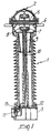
- Figure 1 schematically illustrates an example of a current transformer which is generally used in said configuration.
- the transformer is mainly constituted by three structural components: an insulator 1, generally constituted by a finned tube made of polymeric material or porcelain; a head 2, made of aluminum or steel; and a base 3 which is also made of aluminum or steel and constitutes the structure for anchoring to a supporting surface, for example a supporting pillar.
- the primary winding 5 of the transformer is positioned inside the head 2, as shown in figure 1, and is constituted by a through bar 6 which is arranged horizontally and fixed to the head 2 in a suitable manner.
- the secondary windings 8 of the transformer are arranged inside some toroidal shields 7 and are supported by a supporting tube 9 which is fixed, by means of its lower end, to the base 3 of the transformer. Inside the tube 9, conductors 10 from the secondary windings 8 are conveyed and connected, at their terminals, to a terminal box 11 which is arranged at the base 3 of the transformer.
- a flange 12 between the base 3 and the insulator 1 has holes 13 which are required for the passage of the conductors 10 and for introducing the dielectric gas that arrives from a filling valve (not shown in the figure) provided in the base 3.
- the dielectric gas can be constituted, for example, by sulfur hexafluoride (SF 6 ), nitrogen or a mixture of the two gases.
- the above described current transformer has several problems due to the use of a transformer having a magnetic core.
- the magnetic core of the transformer is in fact affected by saturation effects which compromise the current measurement to be performed.
- the stand-alone transformer configuration has, as described hereinafter, considerable problems in terms of bulk and high costs both during installation and during operation.
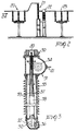
- Figure 2 is a schematic view of an example of use of said stand-alone transformer configuration in a high-voltage substation in which the pole shown in figure 1 can be used as a current transformer.
- the line current flows, for example in the direction of the arrow 24, across a disconnector 20 to a circuit breaker 21 and from there to a current transformer 22, already described in figure 1. Access to the remaining part of the substation is gained by means of the disconnector 23.
- the current transformer 22 can be arranged both upstream and downstream of the circuit breaker 21, but in any case it is arranged outside the circuit breaker 21. In order to ensure adequate insulation, for each electrical pole of the line the transformer 22 must be placed on a separate support and located at a suitable distance from the circuit breaker 21. This entails a considerable overall space occupation of the substation. This fact leads to high installation and operating costs. The plurality of different and separate functional elements inside the substation furthermore entails considerable problems in terms of maintenance and reliability.
- FIG. 3 is a schematic view of an example of configuration in which integration between the circuit breaker and the current transformer is provided in a single pole.
- the circuit breaker/current transformer assembly is mainly constituted by three parts, respectively an interruption chamber 30, shown partially in figure 3, a region 31 which accommodates primary windings and secondary windings 34 of the transformer (provided on a magnetic core), an insulator 33 and a housing 32 which accommodates means 35 for the actuation of the moving contact of the circuit breaker and secondary terminals 36 of the transformer.
- Conductors 37 which protrude from the windings 34 are conveyed through a metal tube 38 located inside the insulator 33 to the secondary terminals 36.
- Said metal tube 38 also accommodates a rod 39 for actuating a moving contact 40 of the circuit breaker.
- the primary current flows from the moving contact 40 to an external primary contact 41 which is located at the region 31 that accommodates the windings 34.
- the pole of figure 3 advantageously mutually integrates the current measurement pole and the circuit breaker, it still uses current transformers wound on a magnetic core.
- the technological problems arising from the use of these components therefore remain.
- said technological problems are essentially the large space occupation and high costs of the windings and the non-ideal magnetic behavior of the core of these transformers.
- poles which allow to solve the problems that arise from the use of windings on magnetic cores.
- These poles use optical technologies and are based on the measurement of the rotation of the polarization plane of a light wave which propagates through a transmission medium in the presence of a magnetic field. The rotation is proportional to the intensity of the magnetic field. This property is commonly known as Faraday effect.
- poles of this type are termed hereinafter "optical current sensors”.
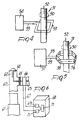
- Figure 4 schematically illustrates a first known constructive example of optical current sensor.
- An optical fiber 53 is wound on a suitable support (not shown in the figure) around a primary conductor 51 through which there flows a current (represented by the arrow 52) to be measured.
- a control system 54 sends a light wave (represented by the arrow 55) which travels along the optical fiber 53.
- the light wave 55 emitted by the control system 54 is influenced by the magnetic field (represented by the dashed arrow 50) generated by the current 52.
- Said light wave 55 returns to the control system 54 with its polarization angle rotated by a certain extent.
- the control system 54 measures this rotation. As already noted, the extent of this rotation is proportional to the magnetic field 50 and therefore to the current 52 that flows along the primary conductor.
- the sensitivity of the optical sensor according to this embodiment depends essentially on the number of turns of the optical fiber 53 around the primary conductor.
- the behavior of the sensor is independent of the geometry of the turns of said optical fiber.
- the transmission medium used is a crystal 56 having a suitable geometry and arranged so as to encircle the primary conductor 51 like a ring.
- a control system 57 emits a light wave (represented by the arrow 58) which, by means of a system of optical fibers 59, reaches the crystal 56.
- the light wave 58 undergoes a series of reflections which make said light wave 58 travel along a path around the primary conductor 51 until it returns through the optical fiber system 59 to the control block 57, which measures the rotation of the polarization plane of the light wave 58.
- This rotation is due to the presence of the magnetic field 50 generated by the current 52 to be measured.
- the extent of said rotation is proportional to the intensity of the magnetic field 50 and therefore to the intensity of the current 52.
- this one is less used because the sensitivity of the sensor can be increased only by increasing the number of internal reflections of the light wave 58 and therefore the dimensions of the crystal 56. This fact can cause, beyond a certain limit, considerable problems in manufacturing said crystal 58.
- the embodiment of figure 5 is therefore used for measuring relatively high currents, for example above 2000 amperes.
- Optical current sensors generally have a high linearity even for very wide current ranges. Accordingly, they allow to advantageously solve the saturation problems that are characteristic of current transformers which have windings on a magnetic core. Furthermore, the use of optical materials such as fibers or crystals allows to ensure adequate insulation while maintaining compact dimensions.
- optical sensors especially those that use an optical fiber as a transmission medium for the light wave, can have highly variable geometries while maintaining their functionality unchanged.
- Another advantage is constituted by the fact that with optical current sensors it is possible to measure AC and DC currents with the same pole.
- optical current sensors are used to measure currents in electric power transmission and/or distribution systems.
- FIG. 6 schematically illustrates a constructive example of a high-voltage pole which uses optical sensors to measure the line current.
- a circuit breaker 60 is mounted on a support 61.
- the line current (represented by the arrow 62) flows in a suitable conductor 64 from the circuit breaker 60 toward a measurement probe 63 which is mounted externally with respect to the structure of the circuit breaker 60 and is insulated from it by means of a retention ring 65 which prevents the escape of the dielectric gas (for example SF 6 ) from the circuit breaker 60.
- the dielectric gas for example SF 6
- the conductor 64 passes through a region in which the optical current sensor 66 is placed so as to be crossed by the conductor 64 in the manner described above in figures 4 and 5.
- Two optical fibers 67 protrude from the optical sensor 66 and are connected to a control block 68 which contains light emitting means 69, light receiving means 70, and a processing block 71.
- Said processing block 71 in addition to controlling the light emitting means 69 and the light receiving means 70, measures the rotation of the polarization plane of the light transmitted along the fibers 67 by the magnetic field generated by the current 62.
- an optical sensor 730 is mounted externally with respect to the body of a circuit breaker 740 at one of the main current conductors (designated by the arrow 750).
- a cable 760 descends along an insulator 770 which is required to provide the adequate spacing between the current conductor 750 and the ground plane which is rigidly coupled to the processing electronics 780.
- the insulator 770 is also used to protect the optical cable 760 against the effects of weather.
- the current sensor can be arranged at the other current conductor 790.
- the aim of the present invention is to provide a pole of a high- and/or medium - voltage circuit breaker which comprises a pole for measuring current which allows to perform very accurate measurements and allows a considerable reduction in space occupation.
- an object of the present invention is to provide a pole of a high- and/or medium -voltage circuit breaker which comprises a current measurement pole in which current measurement occurs without having the non-ideal conditions typical of current measurements performed by means of windings on a core of magnetic material.
- Another object is to provide a pole of a high- and/or medium -voltage circuit breaker which comprises a current measurement pole in which the insertion of said pole entails a reduced number of components required for the practical execution of the structure of said circuit breaker.
- Another object of the present invention is to provide a pole of a high- and/or medium -voltage circuit breaker in which the insertion of a current measurement pole entails a reduced number of mechanical processes to be performed in order to produce the structure in practice.
- Another object of the present invention is to provide a pole of a high- and/or medium -voltage circuit breaker in which the insertion of a current measurement pole entails a reduced number of electrical connections to be performed for the operation of said pole.
- Another object of the present invention is to provide a pole of a high- and/or medium -voltage circuit breaker in which the step for the assembly of said current measurement pole can be performed simply and quickly.
- Another object of the present invention is to provide a pole of a high- and/or medium -voltage circuit breaker which is highly reliable and at competitive costs.
- a pole of a high- and/or medium -voltage circuit breaker comprising an insulating housing, at least one interruption chamber which is positioned inside the insulating housing and contains at least a moving contact and at least a fixed contact, a dielectric gas, and a device for measuring the electric current flowing through the pole, said device comprising:
- the optical current sensor is placed inside the structure of the interruption chamber of the circuit breaker.
- the use of an optical current sensor ensures that the measurement of the electric current occurs accurately, without having the non-ideal conditions typical of known poles which use windings on a magnetic core.
- the pole according to the invention allows to considerably reduce space occupation, using a reduced number of components and electrical connections required for its operation.
- the pole according to the invention is furthermore very easy to assemble, does not require particular mechanical processes for its manufacture, is highly reliable and has relatively low manufacturing costs.
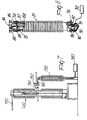
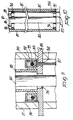
- the pole according to the invention comprises an insulating housing 81, an interruption chamber 80 (shown partially in figure 8) which is positioned inside said insulating housing 81 and contains at least a fixed contact and at least a moving contact, and a housing 82 connected at the base of the insulating housing 81.
- the interruption chamber 80, the insulator 81 and the housing 82 are filled with a dielectric gas, for example SF 6 .
- the interruption chamber 80 accommodates an actuation rod 84 for the moving contact of the circuit breaker (not shown in figure 8).
- the interruption chamber 80 furthermore accommodates a collector 88 which is arranged rigidly with respect to a flange 85.
- An optical current sensor 86 is placed on said flange 85 and around the collector 88; its arrangement is described in detail hereinafter.
- a transmission cable 87 preferably a transmission optical cable containing one or more optical fibers positioned in a protective means, protrudes from the optical sensor 86 and is conveyed toward the housing 82 through a through hole 94 formed in the flange 85.
- Said flange 85 furthermore has a through hole 95 for the passage in the interruption chamber 80 of the actuation rod 84 of the moving contact and of the dielectric gas.
- the collector 88 is arranged so that it is entirely comprised within the optical sensor 86. The current therefore flows from the moving contact of the circuit breaker along the collector 88 up to the flange 85 and is conveyed from there to the outside by means of a suitable terminal, not shown in the figures.
- the path of the current of the circuit breaker lies entirely inside the optical sensor 86.
- the electrical insulation between the sensor 86 and the collector 88 is ensured by virtue of the type itself of the sensor used.
- the optical cable 87 is conveyed into the insulator 81, which also accommodates the actuation rod 84 of the moving contact of the circuit breaker.
- the cable 87 accesses the housing 82 (in which elements 90 for moving the actuation rod 84 are arranged) through a flange 96 which has a through hole 97 for fixing the cable 87 and a through hole 98 for the passage of the actuation rod 84.
- the optical cable 87 then passes through a partition 91 and accesses a control system 92; the partition 91 is conceived so as to ensure the hermetic containment of the dielectric gas.
- the control system 92 can be arranged in an additional chamber (not shown in figure 8) which is rigidly coupled to the body of the circuit breaker and optionally also filled with a dielectric gas or, according to other preferred embodiments, lies outside the body of the circuit breaker, in a seat which can be arranged even at a relatively large distance from the circuit breaker, thus providing a remote-type control.
- the optical sensor 86 comprises, as transmission medium, an optical fiber 99 which is wound in one or more turns around the current collector 88 inside a suitable seat 100: alternatively, it is possible to use, as trasmission medium, an optical crystal arranged so as to encircle the collector 88.
- the seat 100 is arranged around the current collector 88 on the flange 85 and is mechanically isolated from the collector 88 and from said flange 85 by means of an insulating layer of suitable material, for example Poron.
- the optical fiber 99 is immersed in an insulating and supporting layer 102 (for example made of silicone).
- the seat 100 is preferably made of non-conducting material in order to avoid the formation of surface parasitic currents.
- the optical fiber 99 is connected to the optical cable 87 by means of a connector 103 which accesses, by means of the through hole 94, the inside of the insulating housing 81.
- the optical cable 87 contains both ends of the fiber 99 inside an external protective covering made of high-density plastic material, for example kynar.
- the optical cable 87 accesses, by means of the through hole 94, the inside of the insulating housing 81 until it reaches the flange 96 that separates the insulating housing 81 from the housing 82.
- the cable 87 accesses the housing 82.
- the cable 87 is inserted in a protective sheath 104, made for example of metallic material, which is also used to fix the cable 87.
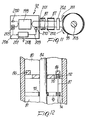
- Figure 11 illustrates an embodiment according to the invention of the control system 92 of figure 8.
- a light source 200 sends to the two ends of the optical fiber 99 two light waves which travel in the directions indicated by the arrows 201 and 202.
- the planar polarization of the waves 201 and 202 occurs by means of a polarizing module 199.
- the optical fiber 99 runs along the optical cable 87 and is wound around a current conductor 203.
- the light waves 201 and 202 before beginning their loop around the conductor 203, are subjected to circular polarization by means of a polarization pole 204.
- each wave acquires a phase delay which depends on the current that flows through the conductor 203. Owing to the opposite directions of travel along the fiber, the respective phase delays of the waves 201 and 202 have opposite signs: this causes an increase in the phase shift between the two light waves, consequently increasing the sensitivity of the measurement.
- the waves 201 and 202 are converted again with a linear polarization by means of the pole 204 and access the block 199, which transmits them to a receiver 205.
- Said receiver 205 measures the phase shift between the two light waves and provides an electric signal 206 which is proportional thereto to a processing block 207 which provides in output a measurement signal 208.
- the processing block 207 also sends a control signal 209 to a phase modulator 210 which closes a feedback cycle inside the system, improving its control.
- Figure 12 schematically illustrates an alternative arrangement of the optical current sensor in the pole according to the invention.
- the optical current sensor 86 is not arranged on the flange 85 between the interruption chamber 80 and the insulating housing 81 of the circuit breaker, but is arranged on a supporting ring 110 which, by virtue of its geometry, can be arranged in any position along the interruption chamber 80.
- the flange 85 and the ring 110 respectively have through holes 94 and 112 for the passage of the optical cable 87.
- Figure 13 illustrates an alternative embodiment of the pole according the invention, in which the optical current sensor 86 is arranged around the structure of the fixed contact 120 of the circuit breaker.
- the optical cable 87 is made to slide along the entire interruption chamber 80 and passes through the flange 85 by virtue of the through hole 121.
- Figure 14 illustrates a further embodiment of the pole according the invention.
- the interruption chamber 80 is arranged substantially horizontal and is mechanically connected to a curved chamber 151 which is arranged on an insulating housing 150.
- the chamber 151 accommodates mechanisms 152 for transmitting motion between a main actuation rod 153 and the actuation rod of the moving contact 154 arranged inside the interruption chamber 80.
- Said interruption chamber 80 also accommodates a fixed contact 155 of the circuit breaker.
- the optical current sensor 86 is arranged inside the chamber 80.
- the arrangements designated respectively by the arrows 156 and 157 appear to be particularly advantageous from the constructive point of view.
- the arrangement indicated by the arrow 157 provides for the placement of the sensor at the fixed contact 155 of the circuit breaker inside the chamber 80.
- the arrangement indicated by the arrow 156 instead provides for the placement, inside the chamber 80, of the optical current sensor 86 at a flange 158 between the interruption chamber 80 and the chamber 151.
- Figure 15 is a view of another embodiment of the invention.
- an interruption chamber 80 of the circuit breaker is used in a metal-clad structure; it comprises a moving contact 161, a fixed contact 162 and field shields 163 which completely surround the moving contact 161 and the fixed contact 162.
- the current of the circuit breaker passes through connections 164 and 165 after passing through the moving contact 161 and the fixed contact 162.
- the optical current sensor 86 is arranged inside the interruption chamber 80 proximate to one of the connections 164 in the position indicated by the arrow 166.
- the optical current sensor 86 can be arranged proximate to the connection 165 in the position indicated by the arrow 167, or it is also possible to use two optical current sensors arranged at both connections 164 and 165.
- the optical cable 87 slides along the interruption chamber and passes through the flanges 168 and 169 through the through holes 170 and 171.
- Figure 16 illustrates another embodiment of the pole according to the invention.
- the electrical pole has two interruption chambers 175 and 176 which are arranged substantially horizontal and contain at least one moving contact and one fixed contact.
- the two chambers 175 and 176 are connected to a support 177 by means of a chamber 178 which contains elements 179 for transmitting motion between a main actuation rod 160 of the circuit breaker and the moving contacts inside the chambers 175 and 176.
- the optical sensor 86 can be arranged inside the structure of each interruption chamber.
- the arrangements designated by arrows 180, 181, 182 and 183 appear to be particularly advantageous and can occur by using one or more optical current sensors.
- the electrical pole of high- and/or medium - voltage grids according to the invention fully achieves the intended aim, since it allows to measure the current of a circuit breaker by using an optical sensor, said optical sensor being integrated in the structure of the pole itself inside the volume occupied by the dielectric gas.
- the insertion of the optical sensor integrally with respect to the structure of the pole occurs with a limited number of components and with a limited number of mechanical processes.
- the pole according to the invention is furthermore easy to assemble, with a considerable reduction in installation costs.
- the pole according to the invention allows a considerable reduction in the space occupation of the electric pole, with a considerable reduction in operating costs.
- Another advantage of the pole according to the invention arises from the fact that the connection between the optical current sensor and the control electronics occurs with a very small number of connections.
Landscapes
- Measuring Instrument Details And Bridges, And Automatic Balancing Devices (AREA)
- Measurement Of Current Or Voltage (AREA)
- Gas-Insulated Switchgears (AREA)
Claims (18)
- Schalterpol eines Hoch- und/oder Mittelspannungs-Leistungsschalters, mit einem isolierenden Gehäuse (81), zumindest einer Unterbrechungskammer (80), die in dem isolierenden Gehäuse (81) angeordnet ist und zumindest einen beweglichen Kontakt und zumindest einen festen Kontakt enthält, einem dielektrischen Gas und einer Vorrichtung zum Messen des durch den Pol fließenden elektrischen Stroms, wobei die Vorrichtung umfaßt:dadurch gekennzeichnet, daß der optische Stromsensor (96) in einem von dem dielektrische Gas eingenommenen Raum des Pols derart angeordnet ist, daß der Weg des Stroms des Leistungsschalters vollkommen innerhalb des optischen Sensors (86) liegt.einen optischen Stromsensor (86), in den eine polarisierte Lichtwelle eintritt; ein Steuersystem (92), das Lichtwellen (55) an den optischen Stromsensor aussendet; und Übertragungsmittel (87, 99), die das Steuersystem (92) mit dem optischen Stromsensor (96) verbinden und entlang denen sich die Lichtwelle bewegt;
- Schalterpol eines Hoch- und/oder Mittelspannungs-Leistungsschalters nach Anspruch 1, dadurch gekennzeichnet, daß das Übertragungsmittel einen Lichtwellenleiter (99) umfaßt.
- Schalterpol eines Hoch- und/oder Mittelspannungs-Leistungsschalters nach Anspruch 2, dadurch gekennzeichnet, daß der Lichtwellenleiter (99) in einem mechanisch isolierenden Mittel positioniert und in einem Sitz (100) aus nichtleitendem Material angeordnet ist.
- Schalterpol eines Hoch- und/oder Mittelspannungs-Leistungsschalters nach einem oder mehreren der vorhergehenden Ansprüche, dadurch gekennzeichnet, daß der optische Stromsensor (86) in der Unterbrechungskammer (80) angeordnet ist.
- Schalterpol eines Hoch- und/oder Mittelspannungs-Leistungsschalters nach einem oder mehreren der vorhergehenden Ansprüche, dadurch gekennzeichnet, daß der optische Stromsensor (86) in der Nähe des festen Kontakts (120) des Leistungsschalters angeordnet ist.
- Schalterpol eines Hoch- und/oder Mittelspannungs-Leistungsschalters nach einem oder mehreren der Ansprüche 1 bis 4, dadurch gekennzeichnet, daß der optische Stromsensor (86) auf einem Ring (110) angeordnet ist, der in einer mittleren Position der Unterbrechungskammer (80) positioniert ist.
- Schalterpol eines Hoch- und/oder Mittelspannungs-Leistungsschalters nach einem oder mehreren der Ansprüche 1 bis 4, dadurch gekennzeichnet, daß der optische Stromsensor (86) an dem beweglichen Kontakt auf einem Flansch (85) angeordnet ist, der die Unterbrechungskammer (80) von dem Rest des Polkörpers trennt.
- Schalterpol eines Hoch- und/oder Mittelspannungs-Leistungsschalters nach einem oder mehreren der Ansprüche 1 bis 4, mit einer metallverkleideten Struktur und einem oder mehreren elektrischen Anschlüssen (164, 165), dadurch gekennzeichnet, daß der optische Stromsensor (86) in der Nähe des einen elektrischen Anschlusses oder der mehreren elektrischen Anschlüsse (164, 165) angeordnet ist.
- Schalterpol eines Hoch- und/oder Mittelspannungs-Leistungsschalters nach einem oder mehreren der Ansprüche 1 bis 4, mit mehreren Unterbrechungskammem (175, 176), dadurch gekennzeichnet, daß der optische Stromsensor (86) innerhalb der Struktur von zumindest einer der Unterbrechungskammem (175, 176) angeordnet ist.
- Schalterpol eines Hoch- und/oder Mittelspannungs-Leistungsschalters nach einem oder mehreren der vorhergehenden Ansprüche, dadurch gekennzeichnet, daß der optische Stromsensor (86) auf einer Schicht aus mechanisch isolierendem Material angeordnet ist.
- Schalterpol eines Hoch- und/oder Mittelspannungs-Leistungsschalters nach Anspruch 1, dadurch gekennzeichnet, daß das Steuersystem (92) ein System (204) zur Polarisation von Licht, ein gyroskopisches Meßsystem und ein Signalverarbeitungssystem (207) umfaßt.
- Schalterpol eines Hoch- und/oder Mittelspannungs-Leistungsschalters nach Anspruch 11, dadurch gekennzeichnet, daß das Steuersystem (92) in einem relativ großen Abstand von dem Pol angeordnet ist.
- Schalterpol eines Hoch- und/oder Mittelspannungs-Leistungsschalters nach Anspruch 11 oder 12 , dadurch gekennzeichnet, daß das Steuersystem (92) in einer Kammer angeordnet ist, die an den Polkörper angrenzt.
- Schalterpol eines Hoch- und/oder Mittelspannungs-Leistungsschalters nach Anspruch 13, dadurch gekennzeichnet, daß die Kammer, die das Steuersystem (92) enthält, fest an den Polkörper gekoppelt und mit einem dielektrischen Gas gefüllt ist.
- Schalterpol eines Hoch- und/oder Mittelspannungs-Leistungsschalters nach einem oder mehreren der vorhergehenden Ansprüche, dadurch gekennzeichnet, daß das Übertragungskabel (87) zumindest über einen Teil seiner Länge in der Struktur des Pols angeordnet ist.
- Schalterpol eines Hoch- und/oder Mittelspannungs-Leistungsschalters nach einem oder mehreren der vorhergehenden Ansprüche, dadurch gekennzeichnet, daß das Übertragungskabel (87) ein optisches Übertragungskabel ist, das einen oder mehrere Lichtwellenleiter (99) enthält, die in ein Schutzmittel getaucht sind.
- Schalterpol eines Hoch- und/oder Mittelspannungs-Leistungsschalters nach Anspruch 1, dadurch gekennzeichnet, daß der optische Stromsensor (86) einen optischen Kristall als Übertragungsmittel enthält.
- Netzstation für Verteiler- und/oder Übertragungsnetze für Hoch- und/oder Mittelspannung, dadurch gekennzeichnet, daß sie einen Schalterpol nach einem oder mehreren der vorhergehenden Ansprüche enthält.
Applications Claiming Priority (3)
| Application Number | Priority Date | Filing Date | Title |
|---|---|---|---|
| ITMI981859 | 1998-08-06 | ||
| IT1998MI001859A IT1302147B1 (it) | 1998-08-06 | 1998-08-06 | Dispositivo ottico integrato per la misura di corrente. |
| PCT/EP1999/005750 WO2000008664A1 (en) | 1998-08-06 | 1999-08-05 | Pole of a circuit breaker with an integrated optical current sensor |
Publications (2)
| Publication Number | Publication Date |
|---|---|
| EP1103059A1 EP1103059A1 (de) | 2001-05-30 |
| EP1103059B1 true EP1103059B1 (de) | 2003-05-21 |
Family
ID=11380635
Family Applications (1)
| Application Number | Title | Priority Date | Filing Date |
|---|---|---|---|
| EP99942820A Revoked EP1103059B1 (de) | 1998-08-06 | 1999-08-05 | Schalterpol mit integriertem optischen stromsensor |
Country Status (8)
| Country | Link |
|---|---|
| US (1) | US6608481B1 (de) |
| EP (1) | EP1103059B1 (de) |
| CN (1) | CN1143339C (de) |
| AT (1) | ATE241210T1 (de) |
| AU (1) | AU766689B2 (de) |
| DE (1) | DE69908138T2 (de) |
| IT (1) | IT1302147B1 (de) |
| WO (1) | WO2000008664A1 (de) |
Families Citing this family (13)
| Publication number | Priority date | Publication date | Assignee | Title |
|---|---|---|---|---|
| AUPQ672300A0 (en) | 2000-04-05 | 2000-05-04 | Nu-Lec Industries Pty Limited | Isolating circuit breaker and circuit protection arrangement |
| EP1851780A1 (de) * | 2005-02-18 | 2007-11-07 | Airpax Corporation, LLC | Schutzschalter mit separatem stromsensor |
| EP1939907A1 (de) * | 2006-12-29 | 2008-07-02 | ABB Technology Ltd | Schutzschalter |
| WO2010012301A1 (en) * | 2008-07-30 | 2010-02-04 | Abb Research Ltd | Generator circuit breaker with fiber-optic current sensor |
| WO2014020621A1 (en) | 2012-08-02 | 2014-02-06 | Alstom Technology Ltd. | Disconnector for high voltage |
| CN105027373B (zh) * | 2013-03-08 | 2019-03-01 | Abb研究有限公司 | 过电流保护装置和方法 |
| EP2784893B1 (de) | 2013-03-29 | 2015-12-09 | Alstom Technology Ltd | Sammelschienenschutz vor Fehlern zwischen Schutzschalter und Stromtransformator |
| DK3084450T3 (en) | 2013-12-20 | 2018-01-15 | Abb Schweiz Ag | Optical sensor |
| CN105810492B (zh) * | 2016-04-08 | 2019-01-01 | 国家电网公司 | 一种断路器 |
| AU2016415342B2 (en) | 2016-07-22 | 2022-06-02 | Abb Power Grids Switzerland Ag | Sensor device having an integrated beam splitter |
| CN108444688B (zh) * | 2018-05-08 | 2023-11-28 | 河南森源电气股份有限公司 | 断路器及断路器用传感器固定装置 |
| EP3614185A1 (de) | 2018-08-24 | 2020-02-26 | ABB Schweiz AG | Faseroptische kabeldurchführung und verfahren zur herstellung davon |
| CA3140589A1 (en) * | 2020-11-20 | 2022-05-20 | Technologies Mindcore Inc. | Gas circuit breaker system and method thereof |
Family Cites Families (6)
| Publication number | Priority date | Publication date | Assignee | Title |
|---|---|---|---|---|
| US3324393A (en) * | 1963-07-26 | 1967-06-06 | Gen Electric | Magneto-optical electric current sensing arrangement |
| FR2049596A5 (de) * | 1969-06-13 | 1971-03-26 | Comp Generale Electricite | |
| FR2668294B1 (fr) * | 1990-10-22 | 1993-09-24 | Alsthom Gec | Disjoncteur a detection d'arc. |
| FR2682527B1 (fr) * | 1991-10-10 | 1993-11-19 | Gec Alsthom Sa | Disjoncteur a enveloppe en materiau composite equipe d'un dispositif de surveillance. |
| DE4312183A1 (de) * | 1993-04-14 | 1994-10-20 | Siemens Ag | Optisches Meßverfahren zum Messen eines elektrischen Wechselstromes mit Temperaturkompensation und Vorrichtung zur Durchführung des Verfahrens |
| FR2731520B1 (fr) * | 1995-03-08 | 1997-04-18 | Gec Alsthom T & D Sa | Mesure de l'intensite electrique dans un appareil subissant un arc electrique |
-
1998
- 1998-08-06 IT IT1998MI001859A patent/IT1302147B1/it active IP Right Grant
-
1999
- 1999-08-05 CN CNB998093343A patent/CN1143339C/zh not_active Expired - Fee Related
- 1999-08-05 EP EP99942820A patent/EP1103059B1/de not_active Revoked
- 1999-08-05 AT AT99942820T patent/ATE241210T1/de not_active IP Right Cessation
- 1999-08-05 WO PCT/EP1999/005750 patent/WO2000008664A1/en not_active Ceased
- 1999-08-05 DE DE69908138T patent/DE69908138T2/de not_active Expired - Fee Related
- 1999-08-05 AU AU56200/99A patent/AU766689B2/en not_active Ceased
- 1999-08-05 US US09/744,953 patent/US6608481B1/en not_active Expired - Lifetime
Also Published As
| Publication number | Publication date |
|---|---|
| AU5620099A (en) | 2000-02-28 |
| ITMI981859A0 (it) | 1998-08-06 |
| WO2000008664A1 (en) | 2000-02-17 |
| DE69908138T2 (de) | 2004-04-08 |
| US6608481B1 (en) | 2003-08-19 |
| ITMI981859A1 (it) | 2000-02-06 |
| DE69908138D1 (de) | 2003-06-26 |
| CN1143339C (zh) | 2004-03-24 |
| CN1311893A (zh) | 2001-09-05 |
| EP1103059A1 (de) | 2001-05-30 |
| ATE241210T1 (de) | 2003-06-15 |
| IT1302147B1 (it) | 2000-07-31 |
| AU766689B2 (en) | 2003-10-23 |
Similar Documents
| Publication | Publication Date | Title |
|---|---|---|
| US6608481B1 (en) | Pole of a circuit breaker with an integrated optical current sensor | |
| EP2909641B1 (de) | Strom- und/oder spannungserfassungsvorrichtung zur integrativen verwendung | |
| US10732206B2 (en) | Current sensor and method of assembly | |
| US6850399B1 (en) | Gas insulated device and failure rating method | |
| US6680665B2 (en) | Three-phase current transformer | |
| US7027280B2 (en) | Gas insulating apparatus and method for locating fault point thereof | |
| US3725741A (en) | Differential transformer mounting arrangement particulary for ground fault interrupter apparatus | |
| JPH10185961A (ja) | 光変流器 | |
| KR102563389B1 (ko) | 가스절연개폐장치의 스페이서 내장 로고우스키형 전류센서의 구조 및 제조 방법 | |
| US20050190032A1 (en) | Compact current transformer casing for gas-insulated switchgear assemblies | |
| US5295207A (en) | Optical apparatus for measuring current in a grounded metal-clad installation | |
| KR100996138B1 (ko) | 광파이버 전류센서를 이용하는 3상 일괄형 gis 스페이서 | |
| NO172959B (no) | Flerfases elektrisk gassekspansjonseffektbryter | |
| KR20220111771A (ko) | 전류 전압 측정 센서 | |
| KR101058319B1 (ko) | 원판형 전극을 이용한 gis 용 용량성 전압 변성기 | |
| KR20210044462A (ko) | 전류측정장치 및 이를 포함하는 가스절연개폐장치 | |
| JP5461260B2 (ja) | 光ファイバ内蔵型絶縁スペーサ | |
| JPS60202365A (ja) | ガス絶縁電気装置 | |
| KR20260001858A (ko) | 스페이서 및 그의 제조방법 | |
| CN119452260A (zh) | 锥形连接器中的低功率仪表互感器(lpit) | |
| JPS63152827A (ja) | ガス遮断器 | |
| JPH10160763A (ja) | 電流の測定構造 | |
| Schmid | Instrument transformers technology and design | |
| JPS60261120A (ja) | 3相一括形ガス絶縁電気機器の電圧電流検出装置 | |
| PL195878B1 (pl) | Przekładnik prądowo-napięciowy |
Legal Events
| Date | Code | Title | Description |
|---|---|---|---|
| PUAI | Public reference made under article 153(3) epc to a published international application that has entered the european phase |
Free format text: ORIGINAL CODE: 0009012 |
|
| 17P | Request for examination filed |
Effective date: 20010209 |
|
| AK | Designated contracting states |
Kind code of ref document: A1 Designated state(s): AT BE CH CY DE DK ES FI FR GB GR IE IT LI LU MC NL PT SE |
|
| 17Q | First examination report despatched |
Effective date: 20010618 |
|
| GRAH | Despatch of communication of intention to grant a patent |
Free format text: ORIGINAL CODE: EPIDOS IGRA |
|
| GRAH | Despatch of communication of intention to grant a patent |
Free format text: ORIGINAL CODE: EPIDOS IGRA |
|
| GRAA | (expected) grant |
Free format text: ORIGINAL CODE: 0009210 |
|
| AK | Designated contracting states |
Designated state(s): AT BE CH CY DE DK ES FI FR GB GR IE IT LI LU MC NL PT SE |
|
| PG25 | Lapsed in a contracting state [announced via postgrant information from national office to epo] |
Ref country code: NL Free format text: LAPSE BECAUSE OF FAILURE TO SUBMIT A TRANSLATION OF THE DESCRIPTION OR TO PAY THE FEE WITHIN THE PRESCRIBED TIME-LIMIT Effective date: 20030521 Ref country code: FI Free format text: LAPSE BECAUSE OF FAILURE TO SUBMIT A TRANSLATION OF THE DESCRIPTION OR TO PAY THE FEE WITHIN THE PRESCRIBED TIME-LIMIT Effective date: 20030521 Ref country code: BE Free format text: LAPSE BECAUSE OF FAILURE TO SUBMIT A TRANSLATION OF THE DESCRIPTION OR TO PAY THE FEE WITHIN THE PRESCRIBED TIME-LIMIT Effective date: 20030521 Ref country code: AT Free format text: LAPSE BECAUSE OF FAILURE TO SUBMIT A TRANSLATION OF THE DESCRIPTION OR TO PAY THE FEE WITHIN THE PRESCRIBED TIME-LIMIT Effective date: 20030521 |
|
| REG | Reference to a national code |
Ref country code: GB Ref legal event code: FG4D |
|
| REG | Reference to a national code |
Ref country code: CH Ref legal event code: EP |
|
| REG | Reference to a national code |
Ref country code: IE Ref legal event code: FG4D |
|
| REF | Corresponds to: |
Ref document number: 69908138 Country of ref document: DE Date of ref document: 20030626 Kind code of ref document: P |
|
| REG | Reference to a national code |
Ref country code: CH Ref legal event code: NV Representative=s name: HEPP, WENGER & RYFFEL AG |
|
| PG25 | Lapsed in a contracting state [announced via postgrant information from national office to epo] |
Ref country code: LU Free format text: LAPSE BECAUSE OF NON-PAYMENT OF DUE FEES Effective date: 20030805 Ref country code: IE Free format text: LAPSE BECAUSE OF NON-PAYMENT OF DUE FEES Effective date: 20030805 Ref country code: CY Free format text: LAPSE BECAUSE OF FAILURE TO SUBMIT A TRANSLATION OF THE DESCRIPTION OR TO PAY THE FEE WITHIN THE PRESCRIBED TIME-LIMIT Effective date: 20030805 |
|
| PG25 | Lapsed in a contracting state [announced via postgrant information from national office to epo] |
Ref country code: SE Free format text: LAPSE BECAUSE OF FAILURE TO SUBMIT A TRANSLATION OF THE DESCRIPTION OR TO PAY THE FEE WITHIN THE PRESCRIBED TIME-LIMIT Effective date: 20030821 Ref country code: PT Free format text: LAPSE BECAUSE OF FAILURE TO SUBMIT A TRANSLATION OF THE DESCRIPTION OR TO PAY THE FEE WITHIN THE PRESCRIBED TIME-LIMIT Effective date: 20030821 Ref country code: GR Free format text: LAPSE BECAUSE OF FAILURE TO SUBMIT A TRANSLATION OF THE DESCRIPTION OR TO PAY THE FEE WITHIN THE PRESCRIBED TIME-LIMIT Effective date: 20030821 Ref country code: DK Free format text: LAPSE BECAUSE OF FAILURE TO SUBMIT A TRANSLATION OF THE DESCRIPTION OR TO PAY THE FEE WITHIN THE PRESCRIBED TIME-LIMIT Effective date: 20030821 |
|
| PG25 | Lapsed in a contracting state [announced via postgrant information from national office to epo] |
Ref country code: MC Free format text: LAPSE BECAUSE OF NON-PAYMENT OF DUE FEES Effective date: 20030831 |
|
| PG25 | Lapsed in a contracting state [announced via postgrant information from national office to epo] |
Ref country code: ES Free format text: LAPSE BECAUSE OF FAILURE TO SUBMIT A TRANSLATION OF THE DESCRIPTION OR TO PAY THE FEE WITHIN THE PRESCRIBED TIME-LIMIT Effective date: 20030901 |
|
| NLV1 | Nl: lapsed or annulled due to failure to fulfill the requirements of art. 29p and 29m of the patents act | ||
| ET | Fr: translation filed | ||
| PLBQ | Unpublished change to opponent data |
Free format text: ORIGINAL CODE: EPIDOS OPPO |
|
| PLBI | Opposition filed |
Free format text: ORIGINAL CODE: 0009260 |
|
| PLAX | Notice of opposition and request to file observation + time limit sent |
Free format text: ORIGINAL CODE: EPIDOSNOBS2 |
|
| 26 | Opposition filed |
Opponent name: AREVA T&D SA Effective date: 20040220 |
|
| REG | Reference to a national code |
Ref country code: IE Ref legal event code: MM4A |
|
| PLAX | Notice of opposition and request to file observation + time limit sent |
Free format text: ORIGINAL CODE: EPIDOSNOBS2 |
|
| PGFP | Annual fee paid to national office [announced via postgrant information from national office to epo] |
Ref country code: GB Payment date: 20040730 Year of fee payment: 6 |
|
| PGFP | Annual fee paid to national office [announced via postgrant information from national office to epo] |
Ref country code: DE Payment date: 20040805 Year of fee payment: 6 |
|
| PGFP | Annual fee paid to national office [announced via postgrant information from national office to epo] |
Ref country code: CH Payment date: 20040806 Year of fee payment: 6 |
|
| PGFP | Annual fee paid to national office [announced via postgrant information from national office to epo] |
Ref country code: FR Payment date: 20040809 Year of fee payment: 6 |
|
| PG25 | Lapsed in a contracting state [announced via postgrant information from national office to epo] |
Ref country code: IT Free format text: LAPSE BECAUSE OF NON-PAYMENT OF DUE FEES Effective date: 20050805 Ref country code: GB Free format text: LAPSE BECAUSE OF NON-PAYMENT OF DUE FEES Effective date: 20050805 |
|
| PG25 | Lapsed in a contracting state [announced via postgrant information from national office to epo] |
Ref country code: LI Free format text: LAPSE BECAUSE OF NON-PAYMENT OF DUE FEES Effective date: 20050831 Ref country code: CH Free format text: LAPSE BECAUSE OF NON-PAYMENT OF DUE FEES Effective date: 20050831 |
|
| PG25 | Lapsed in a contracting state [announced via postgrant information from national office to epo] |
Ref country code: DE Free format text: LAPSE BECAUSE OF NON-PAYMENT OF DUE FEES Effective date: 20060301 |
|
| REG | Reference to a national code |
Ref country code: CH Ref legal event code: PL |
|
| GBPC | Gb: european patent ceased through non-payment of renewal fee |
Effective date: 20050805 |
|
| PG25 | Lapsed in a contracting state [announced via postgrant information from national office to epo] |
Ref country code: FR Free format text: LAPSE BECAUSE OF NON-PAYMENT OF DUE FEES Effective date: 20060428 |
|
| REG | Reference to a national code |
Ref country code: FR Ref legal event code: ST Effective date: 20060428 |
|
| PLBB | Reply of patent proprietor to notice(s) of opposition received |
Free format text: ORIGINAL CODE: EPIDOSNOBS3 |
|
| PLAS | Information related to reply of patent proprietor to notice(s) of opposition deleted |
Free format text: ORIGINAL CODE: EPIDOSDOBS3 |
|
| RDAF | Communication despatched that patent is revoked |
Free format text: ORIGINAL CODE: EPIDOSNREV1 |
|
| RDAG | Patent revoked |
Free format text: ORIGINAL CODE: 0009271 |
|
| STAA | Information on the status of an ep patent application or granted ep patent |
Free format text: STATUS: PATENT REVOKED |
|
| 27W | Patent revoked |
Effective date: 20070407 |