EP1102330A2 - Photovoltaic module - Google Patents
Photovoltaic module Download PDFInfo
- Publication number
- EP1102330A2 EP1102330A2 EP00104539A EP00104539A EP1102330A2 EP 1102330 A2 EP1102330 A2 EP 1102330A2 EP 00104539 A EP00104539 A EP 00104539A EP 00104539 A EP00104539 A EP 00104539A EP 1102330 A2 EP1102330 A2 EP 1102330A2
- Authority
- EP
- European Patent Office
- Prior art keywords
- film
- photovoltaic module
- back cover
- cover film
- resin
- Prior art date
- Legal status (The legal status is an assumption and is not a legal conclusion. Google has not performed a legal analysis and makes no representation as to the accuracy of the status listed.)
- Granted
Links
Images

Classifications
-
- H—ELECTRICITY
- H10—SEMICONDUCTOR DEVICES; ELECTRIC SOLID-STATE DEVICES NOT OTHERWISE PROVIDED FOR
- H10F—INORGANIC SEMICONDUCTOR DEVICES SENSITIVE TO INFRARED RADIATION, LIGHT, ELECTROMAGNETIC RADIATION OF SHORTER WAVELENGTH OR CORPUSCULAR RADIATION
- H10F19/00—Integrated devices, or assemblies of multiple devices, comprising at least one photovoltaic cell covered by group H10F10/00, e.g. photovoltaic modules
- H10F19/30—Integrated devices, or assemblies of multiple devices, comprising at least one photovoltaic cell covered by group H10F10/00, e.g. photovoltaic modules comprising thin-film photovoltaic cells
- H10F19/31—Integrated devices, or assemblies of multiple devices, comprising at least one photovoltaic cell covered by group H10F10/00, e.g. photovoltaic modules comprising thin-film photovoltaic cells having multiple laterally adjacent thin-film photovoltaic cells deposited on the same substrate
-
- H—ELECTRICITY
- H10—SEMICONDUCTOR DEVICES; ELECTRIC SOLID-STATE DEVICES NOT OTHERWISE PROVIDED FOR
- H10F—INORGANIC SEMICONDUCTOR DEVICES SENSITIVE TO INFRARED RADIATION, LIGHT, ELECTROMAGNETIC RADIATION OF SHORTER WAVELENGTH OR CORPUSCULAR RADIATION
- H10F19/00—Integrated devices, or assemblies of multiple devices, comprising at least one photovoltaic cell covered by group H10F10/00, e.g. photovoltaic modules
- H10F19/80—Encapsulations or containers for integrated devices, or assemblies of multiple devices, having photovoltaic cells
-
- H—ELECTRICITY
- H10—SEMICONDUCTOR DEVICES; ELECTRIC SOLID-STATE DEVICES NOT OTHERWISE PROVIDED FOR
- H10F—INORGANIC SEMICONDUCTOR DEVICES SENSITIVE TO INFRARED RADIATION, LIGHT, ELECTROMAGNETIC RADIATION OF SHORTER WAVELENGTH OR CORPUSCULAR RADIATION
- H10F19/00—Integrated devices, or assemblies of multiple devices, comprising at least one photovoltaic cell covered by group H10F10/00, e.g. photovoltaic modules
- H10F19/80—Encapsulations or containers for integrated devices, or assemblies of multiple devices, having photovoltaic cells
- H10F19/85—Protective back sheets
-
- Y—GENERAL TAGGING OF NEW TECHNOLOGICAL DEVELOPMENTS; GENERAL TAGGING OF CROSS-SECTIONAL TECHNOLOGIES SPANNING OVER SEVERAL SECTIONS OF THE IPC; TECHNICAL SUBJECTS COVERED BY FORMER USPC CROSS-REFERENCE ART COLLECTIONS [XRACs] AND DIGESTS
- Y02—TECHNOLOGIES OR APPLICATIONS FOR MITIGATION OR ADAPTATION AGAINST CLIMATE CHANGE
- Y02E—REDUCTION OF GREENHOUSE GAS [GHG] EMISSIONS, RELATED TO ENERGY GENERATION, TRANSMISSION OR DISTRIBUTION
- Y02E10/00—Energy generation through renewable energy sources
- Y02E10/50—Photovoltaic [PV] energy
Definitions
- the present invention relates to a photovoltaic module, particularly, to a photovoltaic module comprising an improved back cover film so as to improve the environmental resistance.
- a photovoltaic module which is arranged on, for example, a roof, is subjected to a severe outdoor environment and, thus, it is strongly required to improve the environmental resistance of solar cells.
- Various materials of constituting members of the photovoltaic module have been studied in order to improve the environmental resistance of the solar cells.
- a thin film photovoltaic module comprises a plurality of solar cells each comprising a transparent electrode layer, a photovoltaic semiconductor layer and a back electrode layer, which are stacked one upon the other on the back surface of a front cover glass.
- the stacked structure formed on the front cover glass is divided into a plurality of strings to form a plurality of solar cells.
- these solar cells are connected to each other in series so as to form an integrated photovoltaic module.
- the back surface of the integrated photovoltaic module is sealed with an encapsulant resin such as an ethylene-vinyl acetate copolymer (EVA). Further, the encapsulant resin are protected by a weather-resistant back cover film laminated thereon.
- EVA ethylene-vinyl acetate copolymer
- a crystalline photovoltaic module comprises 20 to 30 solar cells formed by using a single crystalline semiconductor wafer having a small area and arranged on a front cover glass. These solar cells are connected to each other by wires so as to form the crystalline photovoltaic module.
- the back surface of the crystalline photovoltaic module is sealed with an encapsulant resin such as EVA and is further protected by a back cover film, too.
- a fluorocarbon resin film for example, Tedler manufactured by Du Pont
- a laminate of fluorocarbon resin/aluminum (Al)/fluorocarbon resin or a laminate of fluorocarbon resin/polyethylene terephthalate (PET)/fluorocarbon resin has been used.
- the back cover film consisting of a fluorocarbon resin film alone fails to exhibit a sufficiently high humidity resistance, with the result that the metal members sealed with the encapsulant resin such as an output take-out wire and a back electrode tend to be corroded.
- the presence of the intermediate A1 layer or PET layer enables the laminate of fluorocarbon resin/Al/fluorocarbon resin or the laminate of fluorocarbon resin/PET/fluorocarbon resin to be superior to the film consisting of a fluorocarbon resin alone in the humidity resistance.
- the adhesive strength between the fluorocarbon resin film and the encapsulant resin of EVA is not sufficiently high, with the result that the resin film and the EVA tend to peel from each other over a long period of time. Consequently, the metal members inside the photovoltaic module tend to be corroded because of the moisture intrusion through the peeled portion.
- the conventional photovoltaic module is not satisfactory in the adhesive strength between the encapsulant resin and the back cover film, leaving much room for further improvement of the photovoltaic module in respect of the environmental resistance.
- the intermediate Al layer is exposed to the outside in the case of using a laminate of fluorocarbon resin/Al/fluorocarbon resin, the A1 layer could be brought into contact with the output take-out wire, with the result that the insulation fails to be maintained.
- An object of the present invention is to provide a photovoltaic module excellent in environmental resistance by using a back cover film having a high adhesive strength with an encapsulant resin.
- a photovoltaic module comprising a transparent substrate, solar cells formed on the back surface of the transparent substrate, an encapsulant resin for sealing the solar cells, and a back cover film formed on the back surface of the encapsulant resin, wherein the back cover film comprises at least a multi-layered film of a polyethylene terephthalate-based supporting film and an amorphous polyester-based heat seal layer formed on the surface of the supporting film which is positioned on the side of the encapsulant resin.
- the back cover film may consist of a laminate including a multi-layered film of a polyethylene terephthalate-based supporting film and an amorphous polyester-based heat seal layer, and a fluorocarbon resin film bonded to the back surface of the supporting film constituting the multi-layered film.
- the multi-layered film it is desirable for the multi-layered film to have a thickness of 30 to 100 ⁇ m.
- FIG. 1 is a cross sectional view showing a thin film photovoltaic module of the present invention.
- a stacked structure consisting of a transparent electrode layer 2 made of a transparent conductive oxide (TCO) such as SnO 2 , a photovoltaic semiconductor layer 3 made of silicon or the like, and a back electrode layer 4 made of, for example, Ag is formed on the back surface of a front cover glass 1.
- TCO transparent conductive oxide
- These layers 2, 3, 4 are divided into a plurality of strip-like regions by scribing lines 2a of the transparent electrode layer 2, scribing lines 3a of the photovoltaic semiconductor layer 3 and scribing lines 4a of the back electrode layer 4, the scribing lines 2a, 3a, 4a extending in a direction perpendicular to the paper sheet.
- the transparent electrode 2 of an arbitrary solar cell is connected to the back electrode 4 of the adjacent solar cell 5 via the scribing line 3a of the photovoltaic semiconductor layer 3, and thus the plural solar cells 5 are connected to each other in series so as to form an integrated structure.
- the transparent electrode layer 2 is formed of SnO 2 , ITO, a stack of ITO/SnO 2 , or ZnO.
- the photovoltaic semiconductor layer 3 is formed of a stack of silicon-based semiconductor layers.
- the silicon-based semiconductor includes an amorphous silicon layer (a-Si), a hydrogenated amorphous silicon layer (a-Si:H), a hydrogenated amorphous silicon carbide layer (a-SiC:H), an amorphous silicon nitride layer, and an alloy layer containing silicon and another element such as carbon, germanium or tin.
- the silicon-based semiconductor layers are stacked one upon the other to form a pin-junction, a nip-junction, an ni-junction, a pn-junction, an MIS-junction, a heterojunction, a homojunction, a Schottky junction or a combination of these junctions.
- a CdS-based material, a GaAs-based material, an InP-based material can also be used for forming the photovoltaic semiconductor layer.
- the back electrode layer 4 is formed of a metal film such as Ag or Al film or a stacked film of a metal oxide such as ZnO and a metal film such as Ag or A1.
- the back surface of the integrated photovoltaic module is sealed by an encapsulant resin 6 such as ethylene-vinyl acetate copolymer (EVA) and is further protected by a weather-resistant back cover film 7 laminated on the encapsulant resin 6.
- EVA ethylene-vinyl acetate copolymer
- These encapsulant resin 6 and back cover film 7 are formed by a vacuum laminator.
- other resins such as a silicone resin and polybutyral resin can also be used for forming the encapsulant resin 6.
- FIG. 2 exemplifies the back cover film 7 used in the present invention.
- the back cover film 7 shown in FIG. 2 is of a laminate consisting of a PET-based supporting film 71 and an amorphous PET-based heat seal layer 72.
- the back cover film 7 is arranged such that the heat seal layer 72 is positioned to face the encapsulant resin 6.
- FIG. 3 shows another example of the back cover film 7 used in the present invention.
- the back cover film 7 shown in FIG. 3 comprises the multi-layered film similar to that shown in FIG. 2, which consists of the PET-based supporting film 71 and the amorphous PET-based heat seal layer 72, and a fluorocarbon resin film 73 adhered to the back surface of the supporting film 71 by using, for example, an urethane adhesive.
- a combination of a PET-based supporting film having a thickness of 20 to 100 ⁇ m and an amorphous polyester film having a thickness of 2 to 10 ⁇ m can be suitably used as the multi-layered film of the construction shown in FIG. 2. It is desirable for the supporting film to employ polyethylene terephthalate obtained by condensation between terephthalic acid and ethylene glycol.
- the material of the polyester-based heat seal layer can be suitably selected from amorphous polycondensates between various dicarboxylic acid component and diol component. It is also possible to use an amorphous mixture of the amorphous polyester and a crystalline PET.
- the dicarboxylic acid component of the amorphous polyester which is not particularly limited, includes, for example, terephthalic acid, isophthalic acid, succinic acid, adipic acid, azelaic acid, 1,10decanedicarboxylic acid, sebacic acid, and naphthalene 1,4-dicarboxylic acid.
- the diol component used in the present invention includes, for example, ethylene glycol, propylene glycol, trimethylene glycol, tetramethylene glycol, neopentyl glycol, diethylene glycol and cyclohexane dimethanol. At least one kind of each of dicarboxylic acid components and diol components is selected. It is desirable that the heat seal layer has a glass transition point not higher than 100°C, preferably not higher than 75°C. These multi-layered films can be heat-sealed under temperatures falling within a range of between 140°C and 200°C.
- the materials described above include, for example, Melinex D387, D389 and M342 commercially available from Du Pont.
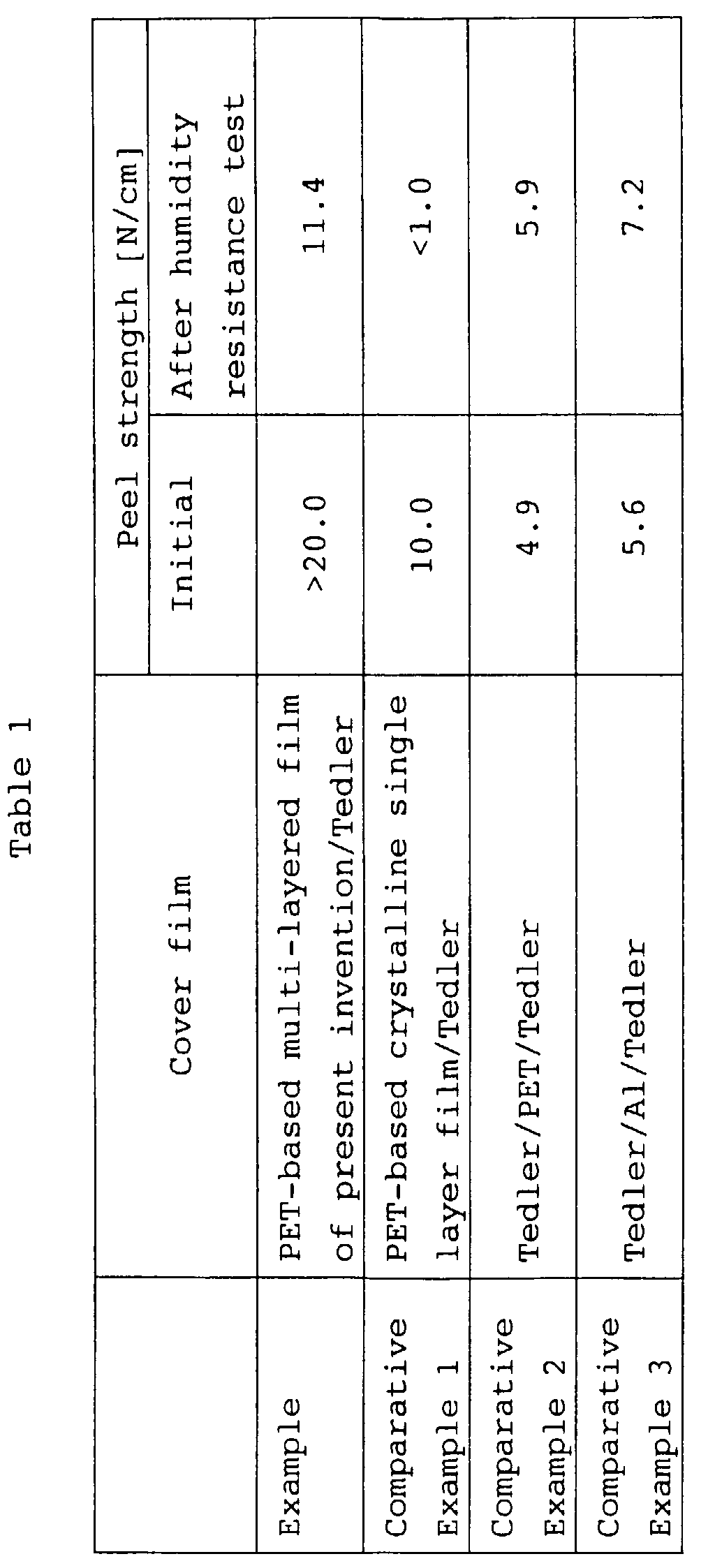
- a peel test was conducted as follows for determining the adhesive strength between the back cover film and the encapsulant resin in respect of the back cover film of the present invention shown in FIG. 3, which consists of the PET-based multi-layered film/fluorocarbon resin film, and the conventional back cover films consisting of a laminate of PET-based crystalline single layer film/fluorocarbon resin film, a laminate of fluorocarbon resin/Al/fluorocarbon resin, and a laminate of fluorocarbon resin/PET/fluorocarbon resin.
- Melinex D387 described above was used as the PET-based multi-layered film.
- Melinex M542 was used as the PET-based crystalline single layer film.
- Tedler was used as the fluorocarbon resin.
- an EVA sheet and Melinex D387 were successively placed on a glass substrate such that the heat seal layer is in contact with the EVA sheet, followed by laminating the structure at 150°C for two hours by using a vacuum laminator.
- additional samples were prepared as above, except that a laminate of Tedler/PET/Tedler or a laminate of Tedler/Al/Tedler was used in place of Melinex D387.
- those portions of the EVA sheet and the cover film which protruded from the periphery of the glass substrate were cut off.
- each of these samples was subjected to a peel test in which the cover film was cut to make two parallel slits with a space of 15 mm and then the cover film alone was peeled in a direction of 90° at a speed of 100 mm/min, thereby force per unit length during the peeling was measured so as to evaluate the initial peel strength at the interface between the EVA layer and the sample.
- a similar peel test was also conducted after each sample was subjected to 10 cycles of humidity resistance test in which each sample was alternately exposed to an environment of 85°C and a relative humidity of 85% and to an environment of -40°C so as to evaluate the peel strength after humidity resistance test. Table 1 shows the results.
- the cover film using a PET-based crystalline single layer film as in Comparative Example 1 substantially failed to exhibit a peel strength after the humidity resistance test, supporting that the cover film had poor environmental resistance.
- the cover film of the Example of the present invention having an amorphous polyester-based heat seal layer exhibited a high initial peel strength and a sufficiently high peel strength even after the humidity resistance test.
- the cover film of the present invention was excellent in its environmental resistance.
- the cover film of the Example of the present invention was also found to be superior to the conventional fluorocarbon resin film (Comparative Examples 2 and 3) in each of the initial peel strength and the peel strength after the humidity resistance test.
- the above description is directed to a thin film photovoltaic module. Needless to say, however, the back cover film of the present invention can also be applied to a crystalline photovoltaic module.
Landscapes
- Photovoltaic Devices (AREA)
- Laminated Bodies (AREA)
- Sealing Material Composition (AREA)
Abstract
Description
Claims (6)
- A photovoltaic module, comprising:characterized in that the back cover film (7) comprises at least a multi-layered film of a polyethylene terephthalate-based supporting film (71) and an amorphous polyester-based heat seal layer (72) formed on the surface of the supporting film (71) which is positioned on the side of the encapsulant resin (6).a transparent substrate (1);solar cells (5) formed on the back surface of the transparent substrate (1);an encapsulant resin (6) for sealing the solar cells (5); anda back cover film (7) formed on the back surface of the encapsulant resin (6),
- The photovoltaic module according to claim 1, characterized in that said back cover film (7) consists of a laminate including a multi-layered film of a polyethylene terephthalate-based supporting film (71) and an amorphous polyester-based heat seal layer (72), and a fluorocarbon resin film (73) bonded to the back surface of the supporting film (71) constituting the multi-layered film.
- The photovoltaic module according to claim 1 or 2, characterized in that said multi-layered film has a thickness of 30 to 100 µm.
- The photovoltaic module according to any of claims 1 to 3, characterized in that said heat seal layer (72) has a glass transition point not higher than 100°C.
- The photovoltaic module according to claim 4, characterized in that said heat seal layer (72) has a glass transition point not higher than 75°C.
- The photovoltaic module according to any of claims 1 to 5, characterized in that said multi-layered film can be heat-sealed under temperatures falling within a range of between 140°C and 200°C.
Applications Claiming Priority (2)
| Application Number | Priority Date | Filing Date | Title |
|---|---|---|---|
| JP33013999 | 1999-11-19 | ||
| JP33013999A JP4459341B2 (en) | 1999-11-19 | 1999-11-19 | Solar cell module |
Publications (3)
| Publication Number | Publication Date |
|---|---|
| EP1102330A2 true EP1102330A2 (en) | 2001-05-23 |
| EP1102330A3 EP1102330A3 (en) | 2006-04-26 |
| EP1102330B1 EP1102330B1 (en) | 2016-01-20 |
Family
ID=18229259
Family Applications (1)
| Application Number | Title | Priority Date | Filing Date |
|---|---|---|---|
| EP00104539.2A Expired - Lifetime EP1102330B1 (en) | 1999-11-19 | 2000-03-13 | Photovoltaic module |
Country Status (4)
| Country | Link |
|---|---|
| US (1) | US6222115B1 (en) |
| EP (1) | EP1102330B1 (en) |
| JP (1) | JP4459341B2 (en) |
| AU (1) | AU771041B2 (en) |
Cited By (2)
| Publication number | Priority date | Publication date | Assignee | Title |
|---|---|---|---|---|
| US8835749B2 (en) | 2007-03-09 | 2014-09-16 | 3M Innovative Properties Company | Multilayer film |
| US10439086B2 (en) | 2014-07-08 | 2019-10-08 | Dupont Teijin Films U.S. Limited Partnership | Polyester film comprising amorphous polyester |
Families Citing this family (38)
| Publication number | Priority date | Publication date | Assignee | Title |
|---|---|---|---|---|
| JP2000294813A (en) * | 1999-04-07 | 2000-10-20 | Bridgestone Corp | Back cover material for solar cell and solar cell |
| EP1071137A3 (en) * | 1999-07-21 | 2007-03-21 | Kaneka Corporation | Roofing tile having photovoltaic module to generate power |
| US6911593B2 (en) * | 2002-09-24 | 2005-06-28 | Board Of Trustees Of The University Of Arkansas | Transparent self-cleaning dust shield |
| DE10393792T5 (en) * | 2002-11-27 | 2005-11-03 | The University Of Toledo, Toledo | Integrated photoelectrochemical cell and system with a liquid electrolyte |
| JP2004288677A (en) * | 2003-03-19 | 2004-10-14 | Sharp Corp | Solar cell module subassembly and double-glazed solar cell module |
| US20070125420A1 (en) * | 2003-08-06 | 2007-06-07 | Fujikura Ltd. | Photoelectric converter and method for manufacturing same |
| JP4194468B2 (en) * | 2003-10-10 | 2008-12-10 | シャープ株式会社 | Solar cell and method for manufacturing the same |
| US7667133B2 (en) * | 2003-10-29 | 2010-02-23 | The University Of Toledo | Hybrid window layer for photovoltaic cells |
| US20060127463A1 (en) * | 2004-12-15 | 2006-06-15 | Nugara Peter N | Composite structure including a low vinyl acetate layer |
| KR101217549B1 (en) * | 2005-02-03 | 2013-01-02 | 삼성전자주식회사 | Nucleic acid purification apparatus containing photovoltaic device, microfluidic apparatus and the purification method using the same |
| WO2006110613A2 (en) * | 2005-04-11 | 2006-10-19 | The University Of Toledo | Integrated photovoltaic-electrolysis cell |
| JP2007048944A (en) * | 2005-08-10 | 2007-02-22 | Toppan Printing Co Ltd | Solar cell backside sealing sheet |
| US7655542B2 (en) * | 2006-06-23 | 2010-02-02 | Applied Materials, Inc. | Methods and apparatus for depositing a microcrystalline silicon film for photovoltaic device |
| US8203071B2 (en) * | 2007-01-18 | 2012-06-19 | Applied Materials, Inc. | Multi-junction solar cells and methods and apparatuses for forming the same |
| US20080173350A1 (en) * | 2007-01-18 | 2008-07-24 | Applied Materials, Inc. | Multi-junction solar cells and methods and apparatuses for forming the same |
| US7582515B2 (en) * | 2007-01-18 | 2009-09-01 | Applied Materials, Inc. | Multi-junction solar cells and methods and apparatuses for forming the same |
| US20080223440A1 (en) * | 2007-01-18 | 2008-09-18 | Shuran Sheng | Multi-junction solar cells and methods and apparatuses for forming the same |
| US20080245414A1 (en) * | 2007-04-09 | 2008-10-09 | Shuran Sheng | Methods for forming a photovoltaic device with low contact resistance |
| US7875486B2 (en) * | 2007-07-10 | 2011-01-25 | Applied Materials, Inc. | Solar cells and methods and apparatuses for forming the same including I-layer and N-layer chamber cleaning |
| US20090104733A1 (en) * | 2007-10-22 | 2009-04-23 | Yong Kee Chae | Microcrystalline silicon deposition for thin film solar applications |
| WO2009059240A1 (en) * | 2007-11-02 | 2009-05-07 | Applied Materials, Inc. | Intrinsic amorphous silicon layer |
| US7741144B2 (en) * | 2007-11-02 | 2010-06-22 | Applied Materials, Inc. | Plasma treatment between deposition processes |
| US20090242020A1 (en) * | 2008-04-01 | 2009-10-01 | Seung-Yeop Myong | Thin-film photovoltaic cell, thin-film photovoltaic module and method of manufacturing thin-film photovoltaic cell |
| KR101476120B1 (en) * | 2008-06-12 | 2014-12-26 | 주성엔지니어링(주) | Thin film solar cell and its manufacturing method |
| US8895842B2 (en) * | 2008-08-29 | 2014-11-25 | Applied Materials, Inc. | High quality TCO-silicon interface contact structure for high efficiency thin film silicon solar cells |
| US20100059110A1 (en) * | 2008-09-11 | 2010-03-11 | Applied Materials, Inc. | Microcrystalline silicon alloys for thin film and wafer based solar applications |
| WO2010079798A1 (en) * | 2009-01-07 | 2010-07-15 | 東洋紡績株式会社 | Polyester film for solar cell back surface protection film |
| KR101393837B1 (en) | 2009-03-31 | 2014-05-13 | 데이진 듀폰 필름 가부시키가이샤 | Laminated polyester film for protection of solar cell undersides |
| US8418418B2 (en) | 2009-04-29 | 2013-04-16 | 3Form, Inc. | Architectural panels with organic photovoltaic interlayers and methods of forming the same |
| KR101039156B1 (en) * | 2009-04-30 | 2011-06-03 | 한양대학교 산학협력단 | Solar cell including carbon nanotube layer |
| WO2011011301A2 (en) * | 2009-07-23 | 2011-01-27 | Applied Materials, Inc. | A mixed silicon phase film for high efficiency thin film silicon solar cells |
| JP5494269B2 (en) * | 2009-09-29 | 2014-05-14 | 東洋紡株式会社 | Polyester film for solar cell back surface protective film |
| WO2011046664A2 (en) * | 2009-10-15 | 2011-04-21 | Applied Materials, Inc. | A barrier layer disposed between a substrate and a transparent conductive oxide layer for thin film silicon solar cells |
| US20110126875A1 (en) * | 2009-12-01 | 2011-06-02 | Hien-Minh Huu Le | Conductive contact layer formed on a transparent conductive layer by a reactive sputter deposition |
| US20110232753A1 (en) * | 2010-03-23 | 2011-09-29 | Applied Materials, Inc. | Methods of forming a thin-film solar energy device |
| WO2012044891A2 (en) * | 2010-09-30 | 2012-04-05 | University Of Delaware | Devices and methods for increasing solar hydrogen conversion efficiency in photovoltaic electrolysis |
| JP2014103310A (en) * | 2012-11-21 | 2014-06-05 | Keiwa Inc | Sheet set for solar cell module back protective plate, solar cell module back protective plate, solar cell module, manufacturing method of solar cell module, sheet for solar cell module back protective plate, and rework method of solar cell module |
| US20150020863A1 (en) * | 2013-07-22 | 2015-01-22 | International Business Machines Corporation | Segmented thin film solar cells |
Family Cites Families (13)
| Publication number | Priority date | Publication date | Assignee | Title |
|---|---|---|---|---|
| US4067764A (en) * | 1977-03-15 | 1978-01-10 | Sierracin Corporation | Method of manufacture of solar cell panel |
| JPS5817685A (en) | 1981-07-24 | 1983-02-01 | Fuji Electric Co Ltd | Resin material for sealing solar cell |
| US4433200A (en) * | 1981-10-02 | 1984-02-21 | Atlantic Richfield Company | Roll formed pan solar module |
| US4526831A (en) * | 1982-06-21 | 1985-07-02 | Edward Hatchadoorian | Process for thermoforming reinforced polymer sheets |
| US4468426A (en) | 1982-11-24 | 1984-08-28 | E. I. Du Pont De Nemours And Company | Adherable reinforced poly(ethylene terephthalate) composite sheet |
| JPS60150658A (en) | 1984-01-18 | 1985-08-08 | Hitachi Ltd | Solar cell module |
| JPH0766441A (en) * | 1993-08-25 | 1995-03-10 | Asahi Glass Co Ltd | Solar cell module |
| KR100235423B1 (en) * | 1993-08-30 | 1999-12-15 | 이.아이,듀우판드네모아앤드캄파니 | Multilayer film having self-limiting heat seal |
| US5478402A (en) * | 1994-02-17 | 1995-12-26 | Ase Americas, Inc. | Solar cell modules and method of making same |
| JP4063896B2 (en) * | 1995-06-20 | 2008-03-19 | 株式会社半導体エネルギー研究所 | Colored see-through photovoltaic device |
| JP3222361B2 (en) * | 1995-08-15 | 2001-10-29 | キヤノン株式会社 | Method of manufacturing solar cell module and solar cell module |
| EP0874404B1 (en) * | 1997-04-21 | 2004-06-30 | Canon Kabushiki Kaisha | Solar cell module and method for manufacturing the same |
| JPH11289103A (en) * | 1998-02-05 | 1999-10-19 | Canon Inc | Semiconductor device, solar cell module and disassembly method thereof |
-
1999
- 1999-11-19 JP JP33013999A patent/JP4459341B2/en not_active Expired - Lifetime
-
2000
- 2000-03-10 AU AU20826/00A patent/AU771041B2/en not_active Ceased
- 2000-03-13 EP EP00104539.2A patent/EP1102330B1/en not_active Expired - Lifetime
- 2000-03-14 US US09/524,633 patent/US6222115B1/en not_active Expired - Lifetime
Cited By (2)
| Publication number | Priority date | Publication date | Assignee | Title |
|---|---|---|---|---|
| US8835749B2 (en) | 2007-03-09 | 2014-09-16 | 3M Innovative Properties Company | Multilayer film |
| US10439086B2 (en) | 2014-07-08 | 2019-10-08 | Dupont Teijin Films U.S. Limited Partnership | Polyester film comprising amorphous polyester |
Also Published As
| Publication number | Publication date |
|---|---|
| AU771041B2 (en) | 2004-03-11 |
| US6222115B1 (en) | 2001-04-24 |
| AU2082600A (en) | 2001-05-24 |
| JP4459341B2 (en) | 2010-04-28 |
| EP1102330A3 (en) | 2006-04-26 |
| JP2001148497A (en) | 2001-05-29 |
| EP1102330B1 (en) | 2016-01-20 |
Similar Documents
| Publication | Publication Date | Title |
|---|---|---|
| EP1102330B1 (en) | Photovoltaic module | |
| US4578526A (en) | Solar module | |
| KR101314698B1 (en) | Backside protective sheet for solar cell and solar cell module comprising the same | |
| US20090260675A1 (en) | Encapsulation of solar modules | |
| US11430903B2 (en) | Multi-junction solar cell module and photovoltaic system | |
| US20120125391A1 (en) | Methods for interconnecting photovoltaic cells | |
| US20110277834A1 (en) | Polymer sheet for solar cell backsheet and solar cell module | |
| JPH10229214A (en) | Solar cell module | |
| JPH08139350A (en) | Solar cell module | |
| JP2003282900A (en) | Solar cell module | |
| EP0874404A2 (en) | Solar cell module and method for manufacturing the same | |
| US20120328869A1 (en) | Solar cell backsheet | |
| US20110197950A1 (en) | Photovoltaic module and method for manufacturing the same | |
| JPH0661518A (en) | Solar cell module | |
| EP3363052A1 (en) | Forming front metal contact on solar cell with enhanced resistance to stress | |
| CN103168416A (en) | Flexible building-integrated photovoltaic structure | |
| JP2006310680A (en) | Thin film solar cell module | |
| JP2007136911A (en) | Sheet for back surface sealing for solar cells | |
| JP2000307137A (en) | Solar cell cover film and solar cell module using the same | |
| JP2010114154A (en) | Backside sealer for photovoltaics, and photovoltaics using the same | |
| JP2009212122A (en) | Rear surface protecting sheet for solar cell and solar cell using this | |
| CN222706898U (en) | High voltage photovoltaic module | |
| CN220121852U (en) | Photovoltaic module | |
| US20130037107A1 (en) | Adhesive layer for photovoltaic module | |
| JP2586868B2 (en) | Solar cell module and method of manufacturing the same |
Legal Events
| Date | Code | Title | Description |
|---|---|---|---|
| PUAI | Public reference made under article 153(3) epc to a published international application that has entered the european phase |
Free format text: ORIGINAL CODE: 0009012 |
|
| AK | Designated contracting states |
Kind code of ref document: A2 Designated state(s): AT BE CH CY DE DK ES FI FR GB GR IE IT LI LU MC NL PT SE |
|
| AX | Request for extension of the european patent |
Free format text: AL;LT;LV;MK;RO;SI |
|
| PUAL | Search report despatched |
Free format text: ORIGINAL CODE: 0009013 |
|
| AK | Designated contracting states |
Kind code of ref document: A3 Designated state(s): AT BE CH CY DE DK ES FI FR GB GR IE IT LI LU MC NL PT SE |
|
| AX | Request for extension of the european patent |
Extension state: AL LT LV MK RO SI |
|
| 17P | Request for examination filed |
Effective date: 20060609 |
|
| AKX | Designation fees paid |
Designated state(s): AT BE CH CY DE DK ES FI FR GB GR IE IT LI LU MC NL PT SE |
|
| 17Q | First examination report despatched |
Effective date: 20070212 |
|
| RAP1 | Party data changed (applicant data changed or rights of an application transferred) |
Owner name: KANEKA CORPORATION |
|
| GRAP | Despatch of communication of intention to grant a patent |
Free format text: ORIGINAL CODE: EPIDOSNIGR1 |
|
| INTG | Intention to grant announced |
Effective date: 20150708 |
|
| GRAS | Grant fee paid |
Free format text: ORIGINAL CODE: EPIDOSNIGR3 |
|
| GRAA | (expected) grant |
Free format text: ORIGINAL CODE: 0009210 |
|
| RAP1 | Party data changed (applicant data changed or rights of an application transferred) |
Owner name: KANEKA CORPORATION |
|
| AK | Designated contracting states |
Kind code of ref document: B1 Designated state(s): AT BE CH CY DE DK ES FI FR GB GR IE IT LI LU MC NL PT SE |
|
| REG | Reference to a national code |
Ref country code: GB Ref legal event code: FG4D |
|
| REG | Reference to a national code |
Ref country code: CH Ref legal event code: EP |
|
| REG | Reference to a national code |
Ref country code: IE Ref legal event code: FG4D |
|
| REG | Reference to a national code |
Ref country code: AT Ref legal event code: REF Ref document number: 772081 Country of ref document: AT Kind code of ref document: T Effective date: 20160215 |
|
| REG | Reference to a national code |
Ref country code: DE Ref legal event code: R096 Ref document number: 60049181 Country of ref document: DE |
|
| REG | Reference to a national code |
Ref country code: NL Ref legal event code: MP Effective date: 20160120 |
|
| REG | Reference to a national code |
Ref country code: AT Ref legal event code: MK05 Ref document number: 772081 Country of ref document: AT Kind code of ref document: T Effective date: 20160120 |
|
| PG25 | Lapsed in a contracting state [announced via postgrant information from national office to epo] |
Ref country code: NL Free format text: LAPSE BECAUSE OF FAILURE TO SUBMIT A TRANSLATION OF THE DESCRIPTION OR TO PAY THE FEE WITHIN THE PRESCRIBED TIME-LIMIT Effective date: 20160120 |
|
| PG25 | Lapsed in a contracting state [announced via postgrant information from national office to epo] |
Ref country code: FI Free format text: LAPSE BECAUSE OF FAILURE TO SUBMIT A TRANSLATION OF THE DESCRIPTION OR TO PAY THE FEE WITHIN THE PRESCRIBED TIME-LIMIT Effective date: 20160120 Ref country code: ES Free format text: LAPSE BECAUSE OF FAILURE TO SUBMIT A TRANSLATION OF THE DESCRIPTION OR TO PAY THE FEE WITHIN THE PRESCRIBED TIME-LIMIT Effective date: 20160120 Ref country code: GR Free format text: LAPSE BECAUSE OF FAILURE TO SUBMIT A TRANSLATION OF THE DESCRIPTION OR TO PAY THE FEE WITHIN THE PRESCRIBED TIME-LIMIT Effective date: 20160421 |
|
| PG25 | Lapsed in a contracting state [announced via postgrant information from national office to epo] |
Ref country code: AT Free format text: LAPSE BECAUSE OF FAILURE TO SUBMIT A TRANSLATION OF THE DESCRIPTION OR TO PAY THE FEE WITHIN THE PRESCRIBED TIME-LIMIT Effective date: 20160120 Ref country code: PT Free format text: LAPSE BECAUSE OF FAILURE TO SUBMIT A TRANSLATION OF THE DESCRIPTION OR TO PAY THE FEE WITHIN THE PRESCRIBED TIME-LIMIT Effective date: 20160520 Ref country code: SE Free format text: LAPSE BECAUSE OF FAILURE TO SUBMIT A TRANSLATION OF THE DESCRIPTION OR TO PAY THE FEE WITHIN THE PRESCRIBED TIME-LIMIT Effective date: 20160120 Ref country code: BE Free format text: LAPSE BECAUSE OF NON-PAYMENT OF DUE FEES Effective date: 20160331 |
|
| REG | Reference to a national code |
Ref country code: DE Ref legal event code: R097 Ref document number: 60049181 Country of ref document: DE |
|
| PG25 | Lapsed in a contracting state [announced via postgrant information from national office to epo] |
Ref country code: MC Free format text: LAPSE BECAUSE OF FAILURE TO SUBMIT A TRANSLATION OF THE DESCRIPTION OR TO PAY THE FEE WITHIN THE PRESCRIBED TIME-LIMIT Effective date: 20160120 Ref country code: LU Free format text: LAPSE BECAUSE OF FAILURE TO SUBMIT A TRANSLATION OF THE DESCRIPTION OR TO PAY THE FEE WITHIN THE PRESCRIBED TIME-LIMIT Effective date: 20160313 Ref country code: DK Free format text: LAPSE BECAUSE OF FAILURE TO SUBMIT A TRANSLATION OF THE DESCRIPTION OR TO PAY THE FEE WITHIN THE PRESCRIBED TIME-LIMIT Effective date: 20160120 |
|
| REG | Reference to a national code |
Ref country code: CH Ref legal event code: PL |
|
| PLBE | No opposition filed within time limit |
Free format text: ORIGINAL CODE: 0009261 |
|
| STAA | Information on the status of an ep patent application or granted ep patent |
Free format text: STATUS: NO OPPOSITION FILED WITHIN TIME LIMIT |
|
| 26N | No opposition filed |
Effective date: 20161021 |
|
| REG | Reference to a national code |
Ref country code: IE Ref legal event code: MM4A |
|
| PG25 | Lapsed in a contracting state [announced via postgrant information from national office to epo] |
Ref country code: BE Free format text: LAPSE BECAUSE OF FAILURE TO SUBMIT A TRANSLATION OF THE DESCRIPTION OR TO PAY THE FEE WITHIN THE PRESCRIBED TIME-LIMIT Effective date: 20160120 |
|
| REG | Reference to a national code |
Ref country code: FR Ref legal event code: ST Effective date: 20161130 |
|
| PG25 | Lapsed in a contracting state [announced via postgrant information from national office to epo] |
Ref country code: CH Free format text: LAPSE BECAUSE OF NON-PAYMENT OF DUE FEES Effective date: 20160331 Ref country code: LI Free format text: LAPSE BECAUSE OF NON-PAYMENT OF DUE FEES Effective date: 20160331 Ref country code: FR Free format text: LAPSE BECAUSE OF NON-PAYMENT OF DUE FEES Effective date: 20160331 Ref country code: IE Free format text: LAPSE BECAUSE OF NON-PAYMENT OF DUE FEES Effective date: 20160313 |
|
| PGFP | Annual fee paid to national office [announced via postgrant information from national office to epo] |
Ref country code: GB Payment date: 20170308 Year of fee payment: 18 |
|
| PGFP | Annual fee paid to national office [announced via postgrant information from national office to epo] |
Ref country code: IT Payment date: 20170320 Year of fee payment: 18 |
|
| PGFP | Annual fee paid to national office [announced via postgrant information from national office to epo] |
Ref country code: DE Payment date: 20180227 Year of fee payment: 19 |
|
| PG25 | Lapsed in a contracting state [announced via postgrant information from national office to epo] |
Ref country code: CY Free format text: LAPSE BECAUSE OF FAILURE TO SUBMIT A TRANSLATION OF THE DESCRIPTION OR TO PAY THE FEE WITHIN THE PRESCRIBED TIME-LIMIT Effective date: 20160120 |
|
| GBPC | Gb: european patent ceased through non-payment of renewal fee |
Effective date: 20180313 |
|
| PG25 | Lapsed in a contracting state [announced via postgrant information from national office to epo] |
Ref country code: GB Free format text: LAPSE BECAUSE OF NON-PAYMENT OF DUE FEES Effective date: 20180313 Ref country code: IT Free format text: LAPSE BECAUSE OF NON-PAYMENT OF DUE FEES Effective date: 20180313 |
|
| REG | Reference to a national code |
Ref country code: DE Ref legal event code: R119 Ref document number: 60049181 Country of ref document: DE |
|
| PG25 | Lapsed in a contracting state [announced via postgrant information from national office to epo] |
Ref country code: DE Free format text: LAPSE BECAUSE OF NON-PAYMENT OF DUE FEES Effective date: 20191001 |