EP1099964A2 - Method for manufacturing polymer optical waveguide - Google Patents
Method for manufacturing polymer optical waveguide Download PDFInfo
- Publication number
- EP1099964A2 EP1099964A2 EP00310057A EP00310057A EP1099964A2 EP 1099964 A2 EP1099964 A2 EP 1099964A2 EP 00310057 A EP00310057 A EP 00310057A EP 00310057 A EP00310057 A EP 00310057A EP 1099964 A2 EP1099964 A2 EP 1099964A2
- Authority
- EP
- European Patent Office
- Prior art keywords
- polymer
- cladding layer
- layer
- mold
- optical waveguide
- Prior art date
- Legal status (The legal status is an assumption and is not a legal conclusion. Google has not performed a legal analysis and makes no representation as to the accuracy of the status listed.)
- Granted
Links
Images



Classifications
-
- G—PHYSICS
- G02—OPTICS
- G02B—OPTICAL ELEMENTS, SYSTEMS OR APPARATUS
- G02B6/00—Light guides; Structural details of arrangements comprising light guides and other optical elements, e.g. couplings
- G02B6/10—Light guides; Structural details of arrangements comprising light guides and other optical elements, e.g. couplings of the optical waveguide type
- G02B6/12—Light guides; Structural details of arrangements comprising light guides and other optical elements, e.g. couplings of the optical waveguide type of the integrated circuit kind
- G02B6/13—Integrated optical circuits characterised by the manufacturing method
-
- G—PHYSICS
- G02—OPTICS
- G02B—OPTICAL ELEMENTS, SYSTEMS OR APPARATUS
- G02B6/00—Light guides; Structural details of arrangements comprising light guides and other optical elements, e.g. couplings
- G02B6/10—Light guides; Structural details of arrangements comprising light guides and other optical elements, e.g. couplings of the optical waveguide type
- G02B6/12—Light guides; Structural details of arrangements comprising light guides and other optical elements, e.g. couplings of the optical waveguide type of the integrated circuit kind
- G02B6/13—Integrated optical circuits characterised by the manufacturing method
- G02B6/138—Integrated optical circuits characterised by the manufacturing method by using polymerisation
-
- B—PERFORMING OPERATIONS; TRANSPORTING
- B29—WORKING OF PLASTICS; WORKING OF SUBSTANCES IN A PLASTIC STATE IN GENERAL
- B29D—PRODUCING PARTICULAR ARTICLES FROM PLASTICS OR FROM SUBSTANCES IN A PLASTIC STATE
- B29D11/00—Producing optical elements, e.g. lenses or prisms
- B29D11/00663—Production of light guides
-
- G—PHYSICS
- G02—OPTICS
- G02B—OPTICAL ELEMENTS, SYSTEMS OR APPARATUS
- G02B6/00—Light guides; Structural details of arrangements comprising light guides and other optical elements, e.g. couplings
- G02B6/10—Light guides; Structural details of arrangements comprising light guides and other optical elements, e.g. couplings of the optical waveguide type
- G02B6/12—Light guides; Structural details of arrangements comprising light guides and other optical elements, e.g. couplings of the optical waveguide type of the integrated circuit kind
- G02B2006/12035—Materials
- G02B2006/12061—Silicon
-
- G—PHYSICS
- G02—OPTICS
- G02B—OPTICAL ELEMENTS, SYSTEMS OR APPARATUS
- G02B6/00—Light guides; Structural details of arrangements comprising light guides and other optical elements, e.g. couplings
- G02B6/10—Light guides; Structural details of arrangements comprising light guides and other optical elements, e.g. couplings of the optical waveguide type
- G02B6/12—Light guides; Structural details of arrangements comprising light guides and other optical elements, e.g. couplings of the optical waveguide type of the integrated circuit kind
- G02B2006/12166—Manufacturing methods
- G02B2006/12176—Etching
Definitions
- the present invention relates to a method for manufacturing a polymer optical waveguide and particularly to a method for manufacturing an optical component such as an optical integrated circuit, optical interconnection, optical coupler or the like.
- Inorganic materials such as quarts glass, multi-component glass or the like, which are characterized by a low optical transmission loss and a wide transmission band, have been widely used as a base material for optical components or optical fibers.
- polymer materials have also been developed and are made attractive as materials for optical waveguides because they are superior in workability and cost to the inorganic materials.
- a flat plate type optical waveguide having a core-clad structure where a core is formed of a polymer with an excellent transparency, such as polymethyl methacrylate (PMMA) or polystyrene, and a cladding layer is formed of a polymer having a refractive index lower than that of the core material (Japanese Unexamined Patent Publication JP-A 3-188402 (1991)).
- a core is formed of a polymer with an excellent transparency, such as polymethyl methacrylate (PMMA) or polystyrene
- a cladding layer is formed of a polymer having a refractive index lower than that of the core material
- An object of the invention is to provide a method for manufacturing an optical waveguide using a mold for reproducing a core profile to attain costless and simple mass-production of a polymer optical waveguide with low loss and high reliability. In order to achieve such object, it is important that polymer films of various thicknesses are completely stripped from the mold without remaining foreign matters.
- the invention provides a method for manufacturing a polymer optical waveguide comprising at least a cladding layer of a first polymer, and a core portion of a second polymer formed in a recessed portion provided on a surface of the cladding layer of the first polymer, the method comprising the steps of: coating the first polymer in molten state or in solution to a molding plate having a projected shape in cross section for forming the core portion, curing the first polymer by ultraviolet rays or by heat, and then stripping the cured first polymer from the molding plate, thereby obtaining the cladding layer having the recessed portion transferred to the surface thereof from the molding plate.
- the thermal resistance required in soldering for mounting electronic components or the like on an obtained optical waveguide substrate can be achieved.
- the first polymer of lower viscosity can be used for transfer, a high fidelity transfer having a transfer rate of approximately 100% can be achieved.
- An optical waveguide substrate can be molded in the form of a film.
- a multi-mode optical waveguide such as one having a core height of 50 ⁇ m and capable of being molded with high aspect ratio can easily be realized.
- the invention also provides a method for manufacturing a polymer optical waveguide comprising at least a cladding layer of a first polymer, and a core portion of a second polymer formed in a recessed portion provided on a surface of the cladding layer of the first polymer, the method comprising the steps of: coating the second polymer in molten state or in solution to a molding plate having a recessed shape in cross section for forming the core portion, curing the second polymer by ultraviolet rays or by heat, thereto applying the first polymer in molten state or in solution, and after curing, stripping the cured first and second polymers from the molding plate.
- the thermal resistance required in soldering for mounting electronic components or the like on an obtained optical waveguide substrate can be achieved.
- the first polymer of lower viscosity can be used for transfer, a high fidelity transfer having a transfer rate of approximately 100% can be achieved.
- An optical waveguide substrate can be molded in the form of a film.
- a multi-mode optical waveguide such as one having a core height of 50 ⁇ m and capable of being molded with high aspect ratio can easily be realized.
- the first or second polymer is coated on the surface of the molding plate after forming a sacrifice layer for facilitating stripping-off of the polymer from the molding plate.
- the core diameter of the mold can be changed.
- the mixing of a release agent is not required. Therefore, the polymer resin can be easily stripped without lowering the optical performance of the resin.
- the molding plate and the polymer are exposed to an atmosphere of liquid or vapor when the first polymer or the second polymer is stripped from the molding plate.
- the mixing of a release agent is not required. Therefore, the polymer resin can be easily stripped without lowering the optical performance of the resin.
- the sacrifice layer is of a silicon oxide and is removed by etching.
- the molding plate is a silicon wafer and the sacrifice layer is of a silicon oxide obtained by thermally oxidizing the silicon wafer.
- the molding plate is of a polymer resin and the cured polymer is stripped from the molding plate by soaking both in a liquid.
- a second cladding layer of a third polymer is formed on the cladding layer and the core portion.
- the methods mentioned above enable easy stripping of a cured polymer from a molding plate and mass-production of polymer optical waveguides of various film thicknesses.
- the polymer for forming upper and lower cladding layers and a core preferably has a Tg (glass transition temperature) of 150°C, more preferably of 200°C, as measured by DSC (differential scanning calorimetry) in an atmosphere of nitrogen at a temperature-raising rate of 10°C/min.
- Tg glass transition temperature
- the substrate having a recess and projection which provides a core portion for the optical waveguide is obtained by applying a process such as plating, plasma etching, chemical etching, laser abrasion or the like to a surface of a substrate formed of a material such as silicon, glass, aluminum, stainless steel or polyimide, or to a surface of a substrate formed of such material and coated with a polymer.
- a process such as plating, plasma etching, chemical etching, laser abrasion or the like to a surface of a substrate formed of a material such as silicon, glass, aluminum, stainless steel or polyimide, or to a surface of a substrate formed of such material and coated with a polymer.
- a film of metal, glass, polymer or the like as a sacrifice layer for stripping the applied polymer from the substrate by vacuum deposition, spattering, plating, thermal oxidation of the substrate or the like. In this manner, a desired mold is obtained.
- the process for stripping the mold and removing the sacrifice layer includes chemical etching or the like.
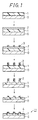
- a method for manufacturing a mold which is obtained by forming a recess and projection on the surface of a polyimide film of a substrate and overlaying a metal film on the polyimide surface is described below.
- a polyamide acid solution which is a precursor of a polyimide, is applied on a surface of a substrate 0 by spin-coating or the like and heated to imide-formation, thereby forming a polyimide layer 1 on the substrate.
- a solvent for the polyamide acid solution is used a polar organic solvent such as N-methyl-2-pyrolidone, N,N-dimethylacetamide, methylsulfoxide or dimethylformamide.
- a mask layer 2 for forming an optical circuit pattern is formed on the polyimide layer 1.
- a metal such as aluminum and titanium, silicon oxide, spin-on glass (SOG), silicon-containing resist, photosensitive polyimide and the like.
- a photoresist After forming the mask layer 2, application of a photoresist, pre-bake, exposure, development andafter-bake are carried out to obtained a patterned resist layer 3. Then, a portion of the mask layer which is not protected by the resist layer 3 is removed by a reactive ion etching or using an etching solution or the like, thereby giving a desired waveguide pattern.
- a silicon-containing resist or a photosensitive polyimide is used for the mask layer 2, the use of a photoresist is not necessary.
- the remaining mask layer 2 is removed by using a reactive ion etching or a release solution.
- a film of a metal such as aluminum, copper or the like is formed on it as a sacrifice layer 4 by vacuum deposition technique, spattering technique or plating technique. In this manner, the desired mold 11 is obtained.
- the layer of silica glass of 10 nm thick is formed by spattering on the substrate having a recess and projection formed thereon. In this manner, the desired mold is obtained.
- a recess and projection corresponding to a core pattern is formed on the silicon wafer using the plasma etching technique or chemical etching technique fully developed as the semiconductor LSI technique.
- silicon oxide is formed. In this manner, the desired mold for manufacturing a polymer optical waveguide can be manufactured.
- a mold for manufacturing a polymer optical waveguide can be manufactured repeatedly by subjecting a silicon wafer to thermal oxidation. Since the thickness of the silica glass layer is as small as 10 nm or less, formable width and depth of groove of the lower cladding layer can be kept within the desired width ⁇ 50 nm even when ten plates are manufactured.
- a reference numeral 11 denotes a mold
- reference numeral 12 a lower cladding layer
- reference numeral 13 a core layer
- reference numeral 14 an upper cladding layer
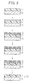
- the reference numeral 11 denotes amold
- a reference numeral 4 a sacrifice layer.
- the lower cladding layer 12 of polyimide is formed on the mold 11 by applying a first polyamide acid solution to the obtained mold 11 for a polymer optical waveguide by spin-coating or the like and heating the applied solution for imide-formation.
- the lower cladding layer is stripped from the mold by etching the sacrifice layer 4 by soaking or the like in a solution which exerts etching effect on the sacrifice layer alone. Then, a surface which has been contacted with the mold is turned upward, and by applying a second polyamide acid solution which is a precursor of a polyimide for forming the core layer 13, to the surface of the lower cladding layer by spin-coating or the like and heating the applied solution for imide-formation, a core layer of polyimide is formed on the lower cladding layer. Then, an excess core layer formed on the lower cladding layer is removed by reactive ion etching or the like.
- a first polyamide acid solution which is a precursor of a polyimide for forming the upper cladding layer 14 is applied by spin-coating or the like and the applied solution is heated for imide-formation.
- a molded-in polymer optical waveguide can be manufactured using a mold for polymer optical waveguide.
- DMAc N,N-dimethylacetamide
- TFDB 2,2-bis(trifluoromethyl)-4,4'-diaminobiphenyl
- a silicon-containing resist layer of 1.5 ⁇ m thick was applied to the polyimide film, and thereafter pre-baked at about 90°C. Then, after subjecting to the contact exposure using a photomask having a 40 line-linear optical waveguide pattern of 6 ⁇ m in width of line and 10 cm in length at 100 ⁇ m intervals, the photoresist on the exposed part was removed by development using a development solution. Then, post-bake was carried out at 90°C. The polyimide film was etched to a depth of 6 ⁇ m from the film surface by oxygen reactive ion etching using the resist layer with patterning as a mask. Then, the resist layer remained in the upper layer of polyimide was removed by a release solution.
- a surface of the lower cladding layer which had been contacted with the mold was turned upward, and by applying about 15 wt% DMAc solution of polyamide acids of 6FDA and 4,4'-oxydianiline (ODA) for forming the core layer to the surface by spin-coating or the like and heating for imide-formation, a core layer of polyimide was formed on the lower cladding layer. Then, an excess core layer formed on the lower cladding layer was removed by the reactive ion etching.
- DMAc solution of polyamide acids of 6FDA and 4,4'-oxydianiline (ODA) for forming the core layer to the surface by spin-coating or the like and heating for imide-formation
- DMAc N,N-dimethylacetamide
- TFDB 2,2-bis (trifluoromethyl)-4,4'-diaminobiphenyl
- a silicon-containing resist layer of 1.5 ⁇ m thick is applied to the polyimide film, and thereafter pre-baked at about 90°C. Then, after subjecting to the contact exposure using a photomask having a 40 line-linear optical waveguide pattern of 6 ⁇ m in width of line and 10 cm in length at 100 ⁇ m intervals, the photoresist on the exposed part was removed by development using a development solution. Then, post-bake was carried out at 90°C. The polyimide film was etched to a depth of 6 ⁇ m from the film surface by oxygen reactive ion etching using the resist layer with patterning as a mask. Then, the resist layer remained in the upper layer of polyimide was removed by a release solution.
- a mold for polymer optical waveguide was manufactured by subjecting a 4 inch-wafer having a ridge of 6 ⁇ m in width and 6 ⁇ m in height formed by plasma etching to thermal oxidation so that a silicon oxide of 10 nm thickn was formed. Then, 15 wt% DMAc solution of polyamide acids of 6FDA and TFDB was coated on the mold by the printing method so that a film of 0.7 mm thick is formed after heating. Thereafter, the polyimide film was stripped from the mold by soaking the mold and all in 2% aqueous hydrofluoric acid solution for etching silicon oxide, thereby forming a lower cladding layer.
- DMAc N,N-dimethylacetamide
- TFDB 2,2-bis(trifluoromethyl)-4,4'-diaminobiphenyl
- a silicon-containing resist layer of 1.5 ⁇ m thick was applied to the polyimide film, and thereafter pre-baked at about 90°C. Then, after subjecting to the contact exposure using a photomask having a 40 line-linear optical waveguide pattern of 6 pm in width of line and 10 cm in length at 100 ⁇ m intervals, the photoresist on the exposed part was removed by development using a development solution. Then, post-bake was carried out at 90°C. The polyimide film was etched to a depth of 6 ⁇ m from the film surface by oxygen reactive ion etching using the resist layer with patterning as a mask. Then, the resist layer remained in the upper layer of polyimide was removed by a release solution.
- a silica glass of 10 nm thick was deposited on the polyimide upper layer by the spattering method.
- the recess and projection of the surface was observed by SEM and it was found that the height and width of a ridge were 6 ⁇ m, respectively, demonstrating that a mold having a desired form could be manufactured.
- the substrate having a recess and projection which provides a core portion for the optical waveguide is obtained by applying a process such as plating, plasma etching, chemical etching, laser abrasion or the like to a surface of a substrate formed of a material such as silicon, glass, aluminum, stainless steel or polyimide, or to a surface of a substrate formed of such material and coated with a polymer.
- a process such as plating, plasma etching, chemical etching, laser abrasion or the like to a surface of a substrate formed of a material such as silicon, glass, aluminum, stainless steel or polyimide, or to a surface of a substrate formed of such material and coated with a polymer.
- a method for manufacturing a mold which is prepared by forming a recess and projection on the surface of a polyimide film of a substrate, is described below with reference to Fig. 3.
- a polyamide acid solution which is a precursor of a polyimide, is applied to a surface of a substrate 0 by spin-coating or the like and heated to imide-formation, thereby forming a polyimide layer 1 on the substrate.
- a solvent for the polyamide acid solution is used a polar organic solvent such as N-methyl-2-pyrolidone, N,N-dimethylacetamide, methylsulfoxide or dimethylformamide.
- a mask layer 2 for forming an optical circuit pattern is formed on the polyimide layer.
- a metal such as aluminum, titanium and the like, silicon oxide, spin-on glass (SOG), silicon-containing resist, photosensitive polyimide and the like.
- a photoresist After forming the mask layer, application of a photoresist, pre-bake, exposure, development and after-bake are carried out to obtained a patterned resist layer 3. Then, a portion of the mask layer which is not protected by the resist layer is removed by a reactive ion etching or using an etching solution or the like, thereby giving a desired waveguide pattern.
- a silicon-containing resist or a photosensitive polyimide is used for the mask layer 2, the use of a photoresist is not necessary.
- the remaining mask layer 2 is removed by using a reactive ion etching or a release solution.
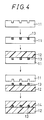
- FIG. 4 An example of steps for a case in which an optical waveguide is manufactured using a mold is shown in the form of a flow chart in Fig. 4.
- the symbol 11 stands for a mold, 12 a lower cladding layer, 13 a core layer, and 14 an upper cladding layer.
- a core layer 13 is embedded in a recessed portion of the mold by applying a first polyamide acid solution to the obtained mold 11 for a polymer optical waveguide by spin-coating or the like and heating it for imide-formation.
- the lower cladding layer 12 is formed by applying a second polyamide acid solution by spin-coating or the like and heating it for imide-formation.
- the polymer is stripped from the mold by soaking in a liquid or by placing in a vapor. This allows manufacturing of a ridge type polymer optical waveguide.
- a surface which has been contacted with the mold is turned upward, and a second polyamide acid solution which is a precursor of a polyimide for forming the upper cladding layer 14 is applied to the surface of the lower cladding layer by spin-coating or the like and it is heated for imide-formation, thereby forming the upper cladding layer.
- a molded-in polymer optical waveguide can be manufactured using a mold for polymer optical waveguide.
- a surface of a glass substrate was etched with C-F etching gas to 6 ⁇ m so that 40 recesses of linear optical waveguide pattern of 6 ⁇ m in width of line and 10 cm in length at 100 ⁇ m intervals.
- the recess and projection of the surface was observed by SEM and it was found that the height and width of grooves were 6 ⁇ m, respectively, demonstrating that a mold having a desired form could be manufactured.
- DMAc N,N-dimethylacetamide
- 6FDA 2, 2-bis (3,4-dicarboxyphenyl)hexafluoropropane dianhydride
- ODA 4,4'-oxydianiline
- a surface which had been contacted with the mold was turned upward, and 15 wt% DMAc solution of polyamide acids of 6FDA and TFDB for forming an upper cladding layer was applied by spin-coating or the like and it was heated for imide-formation, thereby forming the upper cladding layer. In this manner, a molded-in optical waveguide could be manufactured.
- the polyimide film was etched to a depth of 6 ⁇ m from the film surface by oxygen reactive ion etching using the resist layer with patterning as a mask. Then, the resist layer remained in the upper layer of polyimide was removed by a release solution. The recess and projection of the surface was observed by SEM and it was found that the width andheight of a ridge were 6 ⁇ m and 6 ⁇ m, respectively, demonstrating that a mold having a desired form could be manufactured.
- 15 wt% DMAc solution of polyamide acids of 6FDA and ODA for forming a core layer was applied in the recessed portion of the mold by spin-coating method or the like and embedded by heating for imide-formation.
- the polyimide film obtained in this manner had a Tg of 308°C.
- about 15 wt% DMAc polyamide acid solution of 6FDA and TFDB for forming a cladding layer was applied by the printing method so that a cladding layer of 0.7 mm thick is formed after heating and it was heated for imide-formation. Thereafter, the polyimide laminate film was stripped from the mold by soaking in an aqueous solution at room temperature for 10 minutes.
- a surface which had been contacted with the mold was turned upward, and 15 wt% DMAc solution of polyamide acids of 6FDA and TFDB for forming an upper cladding layer was applied by spin-coating or the like and it was heated for imide-formation. In this manner, a molded-in optical waveguide could be manufactured.
- the mold having a recess and projection which provides the core portion for the optical waveguide is one which is processed to give a recess and projection which provides the core portion for the optical waveguide on the surface of a substrate made from silicon, glass, aluminum, stainless steel, polyimide or the like or a substrate surface of polymer coated on these substrate by a process such as plating, plasma etching, chemical etching, laser abrasion or the like.
- a method for manufacturing a mold, which is prepared by forming a recess and projection on the surface of a polyimide film of a substrate, is described below with reference to Fig. 5.
- a polyamide acid solution which is a precursor of a polyimide, is applied to a surface of a substrate 0 by spin-coating or the like and heated to imide-formation, thereby forming a polyimide layer 1 on the substrate.
- a solvent for the polyamide acid solution is used a polar organic solvent such as N-methyl-2-pyrolidone, N,N-dimethylacetamide, methylsulfoxide or dimethylformamide.
- a mask layer 2 for forming an optical circuit pattern is formed on the polyimide layer 1.
- a metal such as aluminum and titanium, silicon oxide, spin-on glass (SOG), silicon-containing resist, photosensitive polyimide and the like.
- a photoresist After forming the mask layer 2, application of a photoresist, pre-bake, exposure, development and after-bake are carried out to obtained a patterned resist layer 3. Then, a portion of the mask layer which is not protected by the resist layer 3 is removed by a reactive ion etching or using an etching solution or the like, thereby giving a desired waveguide pattern.
- a silicon-containing resist or a photosensitive polyimide is used for the mask layer 2, the use of a photoresist is not necessary.
- the remaining mask layer 2 is removed by using a reactive ion etching or a release solution.
- FIG. 6 An example of steps for a case in which an optical waveguide is manufactured using a mold is shown in the form of a flow chart in Fig. 6.
- the symbol 11 stands for a mold, 12 a lower cladding layer, 13 a core layer, and 14 an upper cladding layer.
- a lower cladding layer 12 is formed on the mold by applying a first polyamide acid solution to the obtained mold 11 for polymer optical waveguides by spin-coating or the like and heating it for imide-formation.
- the lower cladding layer is stripped from the mold by possibly soaking in a liquid for 10 minutes.
- a core layer of a polyimide is formed on the lower cladding layer by turning upward a surface which has been contacted with the mold, applying a second polyamide acid solution which is a precursor of a polyimide for forming the core layer 13 to the surface of the lower cladding layer by spin-coating or the like and heating it for imide-formation.
- an excess core layer formed on the lower cladding layer is removed by the reactive ion etching or the like.
- a first polyamide acid solution which is a precursor of a polyimide for forming the upper cladding layer 14 is applied by spin-coating or the like and it is heated for imide-formation.
- a molded-in polymer optical waveguide can be manufactured using a mold for polymer optical waveguides.
- a surface of a glass substrate was etched with C-F etching gas to 6 ⁇ m so that 40 projections of linear optical waveguide pattern of 6 ⁇ m in width of line and 10 cm in length at 100 ⁇ m intervals.
- the recess andprojection of the surface was observed by SEM and it was found that the height and width of grooves were 6 ⁇ m, demonstrating that a mold having a desired form could be manufactured.
- a core layer of polyimide was formed on the lower cladding layer by turning upward a surface which had been contacted with the mold, applying about 15 wt% DMAc solution of polyamide acids of 6FDA and 4,4'-oxydianiline (ODA) for forming a core layer by spin-coating or the like and heating it for imide-formation. Then, an excess core layer formed on the lower cladding layer was removed by the reactive ion etching. Finally, 15 wt% DMAc solution of a polyamide acid of 6FDA and TFDB for forming the upper cladding layer was applied by spin-coating or the like and it is heated for imide-formation. In this manner, a molded-in optical waveguide having a lower cladding layerof 0.1 mm thick could be manufactured.
- ODA 4,4'-oxydianiline
- N,N-dimethylacetamide (DMAc) solution of polyamide acids of pyromellitic acid dianhydride (PMDA) and 4,4'-oxydianiline (ODA) was applied to the polyimide film, and thereafter pre-baked at about 90°C.
- the photoresist on the exposed part was removed by development using a development solution.
- post-bake was carried out at 90°C.
- the polyimide film was etched to a depth of 6 ⁇ m from the film surface by oxygen reactive ion etching using the resist layer with patterning as a mask.
- the resist layer remained in the upper layer of polyimide was removed by a release solution.
- the recess and projection of the surface was observed by SEM and it was found that the height and width of a ridge were 6 ⁇ m, respectively, demonstrating that a mold having a desired form could be manufactured.
- 15 wt% DMAc solution of polyamide acids of 6FDA and TFDB was coated on the mold by the printing method so that a film of 0.7 mm thick is formed after heating. Thereafter, the polyimide film was stripped from the mold by dipping in an aqueous solution. Then, a core layer of polyimide was formed on the lower cladding layer by turning upward a surface which had been contacted with the mold, applying about 15 wt% DMAc solution of polyamide acids of 6FDA and ODA for forming a core layer by spin-coating or the like and heating it for imide-formation. Then, an excess core layer formed on the lower cladding layer was removed by the reactive ion etching.
- the upper and lower cladding layers, the core layer and the polymers used for coating the molding plate substrates are typically polyimide, polyurethane or polyester resins.
- the said first polymer is typically a polyimide, polyurethane or polyester, and is preferably a polyimide.
- the said second polymer is typically a polyimide, polyurethane or polyester, and is preferably a polyimide.
- the said third polymer is typically a polyimide, polyurethane or polyester, and is preferably a polyimide.
- the polymer is typically a polyimide, polyurethane or polyester, and is preferably a polyimide.
Landscapes
- Physics & Mathematics (AREA)
- Engineering & Computer Science (AREA)
- Microelectronics & Electronic Packaging (AREA)
- General Physics & Mathematics (AREA)
- Optics & Photonics (AREA)
- Health & Medical Sciences (AREA)
- Manufacturing & Machinery (AREA)
- Ophthalmology & Optometry (AREA)
- Mechanical Engineering (AREA)
- Optical Integrated Circuits (AREA)
Abstract
Description
coating the first polymer in molten state or in solution to a molding plate having a projected shape in cross section for forming the core portion, curing the first polymer by ultraviolet rays or by heat, and then stripping the cured first polymer from the molding plate, thereby obtaining the cladding layer having the recessed portion transferred to the surface thereof from the molding plate.
coating the second polymer in molten state or in solution to a molding plate having a recessed shape in cross section for forming the core portion, curing the second polymer by ultraviolet rays or by heat, thereto applying the first polymer in molten state or in solution, and after curing, stripping the cured first and second polymers from the molding plate.
2, 2-bis (3,4-dicarboxyphenyl)hexafluoropropane dianhydride (6FDA) and 4,4'-oxydianiline (ODA) for forming a core layer was applied in the recessed portion of the mold by spin-coating method or the like and embedded by heating for imide-formation. In addition, about 15 wt% DMAc polyamide acid solution of 6FDA and 2,2-bis (trifluoromethyl) -4,4'-diaminobiphenyl (TFDB) for forming a cladding layer was applied by the printing method so that a film of 0.1 mm thick is formed after heating and it was heated for imide-formation. Thereafter, the polyimide laminate film was stripped from the mold by soaking in an aqueous solution at room temperature for 10 minutes. A surface which had been contacted with the moldwas turned upward, and 15 wt% DMAc solution of polyamide acids of 6FDA and TFDB for forming an upper cladding layer was applied by spin-coating or the like and it was heated for imide-formation, thereby forming the upper cladding layer. In this manner, a molded-in optical waveguide could be manufactured.
Claims (10)
- A method for manufacturing a polymer optical waveguide comprising at least a cladding layer (12) of a first polymer, and a core portion (13) of a second polymer formed in a recessed portion provided on a surface of the cladding layer (12) of the first polymer, the method comprising the steps of:coating with the first polymer, in molten state or in solution, a molding plate (11) having a projected shape in cross section for forming the core portion (13);curing the first polymer by ultraviolet rays or by heat; andstripping the cured first polymer from the molding plate (11), thereby obtaining the cladding layer (12) having the recessed portion transferred to the surface thereof from the molding plate (11).
- A method for manufacturing a polymer optical waveguide comprising at least a cladding layer (12) of a first polymer, and a core portion (13) of a second polymer formed in a recessed portion provided on a surface of the cladding layer (12) of the first polymer, the method comprising the steps of:coating with the second polymer in molten state or in solution, a molding plate (11) having a recessed shape in cross section for forming the core portion (13);curing the second polymer by ultraviolet rays or by heat, thereto applying the first polymer in molten state or in solution; andafter curing, stripping the cured first and second polymers from the molding plate (11).
- A method according to claim 1 or 2, wherein the first or second polymer is coated on the surface of the molding plate (11) after forming a sacrifice layer (4) for facilitating stripping-off of the polymer from the molding plate (11).
- A method according to any one of the preceding claims, wherein the molding plate (11) and the polymer are exposed to an atmosphere of liquid or vapor when the first polymer or the second polymer is stripped from the molding plate (11).
- A method according to claim 3 or 4, wherein the sacrifice layer (4) is of a silicon oxide and is removed by etching.
- A method according to any one of claims 3 to 5, wherein the molding plate (11) is a silicon wafer and the sacrifice layer (4) is of a silicon oxide obtained by thermally oxidizing the silicon wafer.
- A method according to claim 4, wherein the molding plate (11) is of a polymer resin and the cured polymer is stripped from the molding plate (11) by soaking both in a liquid.
- A method according to any one of the preceding claims, wherein a second cladding layer (14) of a third polymer is formed on the cladding layer (12) and the core portion (13).
- A method according to claim 1, further comprising(d) applying to the cladding layer (12) a said second polymer in molten state or in solution;(e) optionally removing excess second polymer from the surface of the cladding layer; and(f) curing the second polymer.
- A method for manufacturing an optical integrated circuit, optical interconnection or optic coupler, which method comprises:(a) manufacturing a polymer optical waveguide by a process according to any one of the preceding claims; and(b) incorporating the thus obtained waveguide into an optical integrated circuit, optical interconnection or optic coupler.
Applications Claiming Priority (4)
| Application Number | Priority Date | Filing Date | Title |
|---|---|---|---|
| JP32082299 | 1999-11-11 | ||
| JP32082299 | 1999-11-11 | ||
| JP2000082191 | 2000-03-23 | ||
| JP2000082191 | 2000-03-23 |
Publications (3)
| Publication Number | Publication Date |
|---|---|
| EP1099964A2 true EP1099964A2 (en) | 2001-05-16 |
| EP1099964A3 EP1099964A3 (en) | 2002-06-19 |
| EP1099964B1 EP1099964B1 (en) | 2008-07-09 |
Family
ID=26570219
Family Applications (1)
| Application Number | Title | Priority Date | Filing Date |
|---|---|---|---|
| EP00310057A Expired - Lifetime EP1099964B1 (en) | 1999-11-11 | 2000-11-13 | Method for manufacturing polymer optical waveguide |
Country Status (5)
| Country | Link |
|---|---|
| US (1) | US6500603B1 (en) |
| EP (1) | EP1099964B1 (en) |
| KR (1) | KR100362829B1 (en) |
| CA (1) | CA2325679A1 (en) |
| DE (1) | DE60039401D1 (en) |
Cited By (4)
| Publication number | Priority date | Publication date | Assignee | Title |
|---|---|---|---|---|
| EP1298462A3 (en) * | 2001-09-28 | 2004-06-16 | Omron Corporation | Optical wave guide and method for producing the same |
| US7050691B2 (en) * | 2002-09-20 | 2006-05-23 | Toppan Printing Co., Ltd. | Optical waveguide and method of manufacturing the same |
| US7455971B2 (en) | 1998-06-24 | 2008-11-25 | Illumina, Inc. | Multiplex decoding of array sensors with microspheres |
| WO2012154026A1 (en) * | 2011-05-12 | 2012-11-15 | Mimos Bhd. | A method of forming structures in polymer films |
Families Citing this family (50)
| Publication number | Priority date | Publication date | Assignee | Title |
|---|---|---|---|---|
| US7087179B2 (en) * | 2000-12-11 | 2006-08-08 | Applied Materials, Inc. | Optical integrated circuits (ICs) |
| US7413688B2 (en) * | 2001-09-17 | 2008-08-19 | Kenneth Noddings | Fabrication of optical devices and assemblies |
| JP2003172841A (en) * | 2001-09-28 | 2003-06-20 | Omron Corp | Optical waveguide and method of manufacturing the same |
| US7132736B2 (en) | 2001-10-31 | 2006-11-07 | Georgia Tech Research Corporation | Devices having compliant wafer-level packages with pillars and methods of fabrication |
| US7518737B2 (en) * | 2002-03-29 | 2009-04-14 | Georgia Tech Research Corp. | Displacement-measuring optical device with orifice |
| US7440117B2 (en) * | 2002-03-29 | 2008-10-21 | Georgia Tech Research Corp. | Highly-sensitive displacement-measuring optical device |
| US7135777B2 (en) * | 2002-05-03 | 2006-11-14 | Georgia Tech Research Corporation | Devices having compliant wafer-level input/output interconnections and packages using pillars and methods of fabrication thereof |
| US7099525B2 (en) * | 2002-08-26 | 2006-08-29 | Georgia Tech Research Corporation | Dual-mode/function optical and electrical interconnects, methods of fabrication thereof, and methods of use thereof |
| JP2004144987A (en) * | 2002-10-24 | 2004-05-20 | Fuji Xerox Co Ltd | Manufacturing method of polymeric optical waveguide |
| US20040184704A1 (en) * | 2003-03-17 | 2004-09-23 | Bakir Muhannad S. | Curved metal-polymer dual-mode/function optical and electrical interconnects, methods of fabrication thereof, and uses thereof |
| JP4175183B2 (en) * | 2003-06-04 | 2008-11-05 | 富士ゼロックス株式会社 | Method for producing polymer optical waveguide |
| US20050257709A1 (en) * | 2003-08-28 | 2005-11-24 | Tony Mule | Systems and methods for three-dimensional lithography and nano-indentation |
| JP2005181662A (en) * | 2003-12-19 | 2005-07-07 | Fuji Xerox Co Ltd | Method for manufacturing macromolecular optical waveguide |
| JP4225207B2 (en) * | 2004-01-23 | 2009-02-18 | 富士ゼロックス株式会社 | Method for producing polymer optical waveguide |
| JP4067504B2 (en) * | 2004-03-17 | 2008-03-26 | 三洋電機株式会社 | Optical waveguide and manufacturing method thereof |
| JP2006030919A (en) * | 2004-07-22 | 2006-02-02 | Kansai Paint Co Ltd | Method of manufacturing optical waveguide |
| US7283695B2 (en) * | 2004-08-31 | 2007-10-16 | Georgia Tech Research Corporation | Optical interconnects in microelectronics based on azimuthally asymmetric long-period fiber grating couplers |
| US7266267B2 (en) * | 2004-11-16 | 2007-09-04 | Georgia Tech Research Corp. | Microfluidic, optical, and electrical input output interconnects, methods of fabrication thereof, and methods of use thereof |
| JP2014029386A (en) * | 2012-07-31 | 2014-02-13 | International Business Maschines Corporation | Method for producing polymer waveguide array assembly of single mode |
| WO2014065304A1 (en) * | 2012-10-26 | 2014-05-01 | 三菱レイヨン株式会社 | Light-guiding body, light-guiding body fabrication method, optical shutter, and planar light source device |
| JP2019162565A (en) * | 2016-07-25 | 2019-09-26 | 富士フイルム株式会社 | Gas separation membrane, gas separation membrane module and gas separator |
| US10224224B2 (en) | 2017-03-10 | 2019-03-05 | Micromaterials, LLC | High pressure wafer processing systems and related methods |
| US10622214B2 (en) | 2017-05-25 | 2020-04-14 | Applied Materials, Inc. | Tungsten defluorination by high pressure treatment |
| CN110678973B (en) | 2017-06-02 | 2023-09-19 | 应用材料公司 | Dry stripping of boron carbide hard masks |
| US10269571B2 (en) | 2017-07-12 | 2019-04-23 | Applied Materials, Inc. | Methods for fabricating nanowire for semiconductor applications |
| US10234630B2 (en) * | 2017-07-12 | 2019-03-19 | Applied Materials, Inc. | Method for creating a high refractive index wave guide |
| US10179941B1 (en) | 2017-07-14 | 2019-01-15 | Applied Materials, Inc. | Gas delivery system for high pressure processing chamber |
| KR102405723B1 (en) | 2017-08-18 | 2022-06-07 | 어플라이드 머티어리얼스, 인코포레이티드 | High pressure and high temperature annealing chamber |
| US10276411B2 (en) | 2017-08-18 | 2019-04-30 | Applied Materials, Inc. | High pressure and high temperature anneal chamber |
| WO2019055415A1 (en) | 2017-09-12 | 2019-03-21 | Applied Materials, Inc. | Apparatus and methods for manufacturing semiconductor structures using protective barrier layer |
| US10643867B2 (en) | 2017-11-03 | 2020-05-05 | Applied Materials, Inc. | Annealing system and method |
| EP3707746B1 (en) | 2017-11-11 | 2023-12-27 | Micromaterials LLC | Gas delivery system for high pressure processing chamber |
| WO2019099125A1 (en) | 2017-11-16 | 2019-05-23 | Applied Materials, Inc. | High pressure steam anneal processing apparatus |
| JP2021503714A (en) | 2017-11-17 | 2021-02-12 | アプライド マテリアルズ インコーポレイテッドApplied Materials,Incorporated | Capacitor system for high pressure processing system |
| JP7299898B2 (en) | 2018-01-24 | 2023-06-28 | アプライド マテリアルズ インコーポレイテッド | Seam repair using high pressure annealing |
| KR102702244B1 (en) | 2018-03-09 | 2024-09-03 | 어플라이드 머티어리얼스, 인코포레이티드 | High pressure annealing process for metal containing materials |
| US10714331B2 (en) | 2018-04-04 | 2020-07-14 | Applied Materials, Inc. | Method to fabricate thermally stable low K-FinFET spacer |
| US10950429B2 (en) | 2018-05-08 | 2021-03-16 | Applied Materials, Inc. | Methods of forming amorphous carbon hard mask layers and hard mask layers formed therefrom |
| US10566188B2 (en) | 2018-05-17 | 2020-02-18 | Applied Materials, Inc. | Method to improve film stability |
| US10704141B2 (en) | 2018-06-01 | 2020-07-07 | Applied Materials, Inc. | In-situ CVD and ALD coating of chamber to control metal contamination |
| US10748783B2 (en) | 2018-07-25 | 2020-08-18 | Applied Materials, Inc. | Gas delivery module |
| US10675581B2 (en) | 2018-08-06 | 2020-06-09 | Applied Materials, Inc. | Gas abatement apparatus |
| JP7179172B6 (en) | 2018-10-30 | 2022-12-16 | アプライド マテリアルズ インコーポレイテッド | Method for etching structures for semiconductor applications |
| CN112996950B (en) | 2018-11-16 | 2024-04-05 | 应用材料公司 | Film deposition using enhanced diffusion process |
| WO2020117462A1 (en) | 2018-12-07 | 2020-06-11 | Applied Materials, Inc. | Semiconductor processing system |
| DE102020109869A1 (en) | 2019-05-03 | 2020-11-05 | Docter Optics Se | Process for the production of an optical element from glass |
| US11901222B2 (en) | 2020-02-17 | 2024-02-13 | Applied Materials, Inc. | Multi-step process for flowable gap-fill film |
| CN112379480B (en) * | 2020-11-17 | 2022-05-24 | 济南晶正电子科技有限公司 | Preparation method of waveguide structure composite substrate, composite substrate and photoelectric crystal film |
| CN114488399A (en) * | 2022-01-30 | 2022-05-13 | 华中科技大学 | Template for preparing optical waveguide device and preparation method and application thereof |
| CN116160593A (en) * | 2022-12-21 | 2023-05-26 | 深圳珑璟光电科技有限公司 | Grating waveguide mold, manufacturing method thereof, grating waveguide and near-eye display device |
Family Cites Families (11)
| Publication number | Priority date | Publication date | Assignee | Title |
|---|---|---|---|---|
| US4116753A (en) | 1976-06-14 | 1978-09-26 | Olympus Optical Co., Ltd. | Method for the manufacture of optical mold for reproducing curved surfaces having the same shape as an optical prototype |
| JPS57155507A (en) | 1981-03-20 | 1982-09-25 | Fuji Photo Film Co Ltd | Manufacture of high density photoconductive sheet |
| JPS61138903A (en) | 1984-12-12 | 1986-06-26 | Nippon Telegr & Teleph Corp <Ntt> | Production of optical waveguide |
| JPH02191906A (en) * | 1988-10-20 | 1990-07-27 | Matsushita Electric Ind Co Ltd | Method of manufacturing optical waveguide |
| JP2599497B2 (en) | 1989-09-27 | 1997-04-09 | 日本電信電話株式会社 | Flat plastic optical waveguide |
| JP2813713B2 (en) | 1990-04-27 | 1998-10-22 | 日本電信電話株式会社 | Polyimide optical waveguide |
| US5265184A (en) | 1992-05-28 | 1993-11-23 | Motorola, Inc. | Molded waveguide and method for making same |
| JPH09189818A (en) * | 1996-01-10 | 1997-07-22 | Nippon Telegr & Teleph Corp <Ntt> | Method for producing mold for producing polymer optical waveguide |
| JPH09281351A (en) | 1996-04-18 | 1997-10-31 | Sharp Corp | Method for manufacturing polymer optical waveguide |
| JP3188402B2 (en) | 1996-10-02 | 2001-07-16 | 有限会社トーカイタック | Walnut button |
| JPH10221556A (en) | 1997-02-05 | 1998-08-21 | Sharp Corp | Manufacturing method of optical waveguide |
-
2000
- 2000-11-09 US US09/708,520 patent/US6500603B1/en not_active Expired - Fee Related
- 2000-11-10 KR KR1020000066733A patent/KR100362829B1/en not_active Expired - Fee Related
- 2000-11-10 CA CA002325679A patent/CA2325679A1/en not_active Abandoned
- 2000-11-13 DE DE60039401T patent/DE60039401D1/en not_active Expired - Lifetime
- 2000-11-13 EP EP00310057A patent/EP1099964B1/en not_active Expired - Lifetime
Cited By (6)
| Publication number | Priority date | Publication date | Assignee | Title |
|---|---|---|---|---|
| US7455971B2 (en) | 1998-06-24 | 2008-11-25 | Illumina, Inc. | Multiplex decoding of array sensors with microspheres |
| US8460865B2 (en) | 1998-06-24 | 2013-06-11 | Illumina, Inc. | Multiplex decoding of array sensors with microspheres |
| EP1298462A3 (en) * | 2001-09-28 | 2004-06-16 | Omron Corporation | Optical wave guide and method for producing the same |
| US7050691B2 (en) * | 2002-09-20 | 2006-05-23 | Toppan Printing Co., Ltd. | Optical waveguide and method of manufacturing the same |
| US7289713B2 (en) | 2002-09-20 | 2007-10-30 | Toppan Printing Co., Ltd. | Optical waveguide and method of manufacturing the same |
| WO2012154026A1 (en) * | 2011-05-12 | 2012-11-15 | Mimos Bhd. | A method of forming structures in polymer films |
Also Published As
| Publication number | Publication date |
|---|---|
| KR20010060293A (en) | 2001-07-06 |
| EP1099964A3 (en) | 2002-06-19 |
| EP1099964B1 (en) | 2008-07-09 |
| US6500603B1 (en) | 2002-12-31 |
| DE60039401D1 (en) | 2008-08-21 |
| CA2325679A1 (en) | 2001-05-11 |
| KR100362829B1 (en) | 2002-11-29 |
Similar Documents
| Publication | Publication Date | Title |
|---|---|---|
| US6500603B1 (en) | Method for manufacturing polymer optical waveguide | |
| EP0616234B1 (en) | Method of manufacturing a polyimide optical waveguide | |
| JP3947457B2 (en) | Manufacturing method of polyimide optical waveguide | |
| JP4799764B2 (en) | Photosensitive polyimide precursor composition for optical waveguide, photosensitive polyimide composition for optical waveguide, and optical waveguide using the same | |
| KR100976671B1 (en) | Manufacturing method of optical waveguide | |
| JP3943827B2 (en) | Method for producing polymer optical waveguide | |
| JP3327356B2 (en) | Fluorinated polyimide optical waveguide and method for manufacturing the same | |
| JPH09251113A (en) | Heat resistant high refractive index difference polymer optical waveguide and method for manufacturing the same | |
| US20080128929A1 (en) | Method for Manufacturing Optical Devices | |
| JP2001318257A (en) | Method for producing polymeric optical waveguide | |
| JP2002277663A (en) | Method for manufacturing optical waveguide | |
| JP2816771B2 (en) | Polyimide optical waveguide and method of manufacturing the same | |
| JP2000056147A (en) | Method for manufacturing polymer optical waveguide | |
| JP2003248311A (en) | Photosensitive polyimide resin precursor composition, optical polyimide and optical waveguide obtained therefrom | |
| JP2001074949A (en) | Optical waveguide made of resin with protective layer, its production and optical parts | |
| EP1778462B1 (en) | Method for manufacturing optical devices | |
| JP2002148455A (en) | Polymer optical waveguide device | |
| JP4310795B2 (en) | RESIN OPTICAL WAVEGUIDE PROVIDED WITH FLATTING LAYER, ITS MANUFACTURING METHOD, AND OPTICAL COMPONENT | |
| JPH06347658A (en) | Plastic optical waveguide | |
| JP3335276B2 (en) | Method for manufacturing polymer optical waveguide | |
| JP2003172838A (en) | Optical waveguide device and method of manufacturing the same | |
| JP2000321456A (en) | Production of polyimide optical waveguide | |
| JPH09189818A (en) | Method for producing mold for producing polymer optical waveguide | |
| JP2005103952A (en) | Transfer mold and optical waveguide manufacturing method | |
| JP2005189646A (en) | Optical waveguide |
Legal Events
| Date | Code | Title | Description |
|---|---|---|---|
| PUAI | Public reference made under article 153(3) epc to a published international application that has entered the european phase |
Free format text: ORIGINAL CODE: 0009012 |
|
| AK | Designated contracting states |
Kind code of ref document: A2 Designated state(s): AT BE CH CY DE DK ES FI FR GB GR IE IT LI LU MC NL PT SE TR |
|
| AX | Request for extension of the european patent |
Free format text: AL;LT;LV;MK;RO;SI |
|
| PUAL | Search report despatched |
Free format text: ORIGINAL CODE: 0009013 |
|
| AK | Designated contracting states |
Kind code of ref document: A3 Designated state(s): AT BE CH CY DE DK ES FI FR GB GR IE IT LI LU MC NL PT SE TR |
|
| AX | Request for extension of the european patent |
Free format text: AL;LT;LV;MK;RO;SI |
|
| 17P | Request for examination filed |
Effective date: 20021121 |
|
| 17Q | First examination report despatched |
Effective date: 20030120 |
|
| AKX | Designation fees paid |
Designated state(s): DE FR GB |
|
| RAP1 | Party data changed (applicant data changed or rights of an application transferred) |
Owner name: MITSUI CHEMICALS, INC. |
|
| GRAP | Despatch of communication of intention to grant a patent |
Free format text: ORIGINAL CODE: EPIDOSNIGR1 |
|
| GRAS | Grant fee paid |
Free format text: ORIGINAL CODE: EPIDOSNIGR3 |
|
| GRAA | (expected) grant |
Free format text: ORIGINAL CODE: 0009210 |
|
| AK | Designated contracting states |
Kind code of ref document: B1 Designated state(s): DE FR GB |
|
| REG | Reference to a national code |
Ref country code: GB Ref legal event code: FG4D |
|
| REF | Corresponds to: |
Ref document number: 60039401 Country of ref document: DE Date of ref document: 20080821 Kind code of ref document: P |
|
| PLBE | No opposition filed within time limit |
Free format text: ORIGINAL CODE: 0009261 |
|
| STAA | Information on the status of an ep patent application or granted ep patent |
Free format text: STATUS: NO OPPOSITION FILED WITHIN TIME LIMIT |
|
| 26N | No opposition filed |
Effective date: 20090414 |
|
| GBPC | Gb: european patent ceased through non-payment of renewal fee |
Effective date: 20081113 |
|
| REG | Reference to a national code |
Ref country code: FR Ref legal event code: ST Effective date: 20090731 |
|
| PG25 | Lapsed in a contracting state [announced via postgrant information from national office to epo] |
Ref country code: GB Free format text: LAPSE BECAUSE OF NON-PAYMENT OF DUE FEES Effective date: 20081113 |
|
| PG25 | Lapsed in a contracting state [announced via postgrant information from national office to epo] |
Ref country code: FR Free format text: LAPSE BECAUSE OF NON-PAYMENT OF DUE FEES Effective date: 20081130 |
|
| PGFP | Annual fee paid to national office [announced via postgrant information from national office to epo] |
Ref country code: DE Payment date: 20131106 Year of fee payment: 14 |
|
| REG | Reference to a national code |
Ref country code: DE Ref legal event code: R119 Ref document number: 60039401 Country of ref document: DE |
|
| PG25 | Lapsed in a contracting state [announced via postgrant information from national office to epo] |
Ref country code: DE Free format text: LAPSE BECAUSE OF NON-PAYMENT OF DUE FEES Effective date: 20150602 |