EP1099953A2 - Semiconductor device with testing capability - Google Patents
Semiconductor device with testing capability Download PDFInfo
- Publication number
- EP1099953A2 EP1099953A2 EP00305720A EP00305720A EP1099953A2 EP 1099953 A2 EP1099953 A2 EP 1099953A2 EP 00305720 A EP00305720 A EP 00305720A EP 00305720 A EP00305720 A EP 00305720A EP 1099953 A2 EP1099953 A2 EP 1099953A2
- Authority
- EP
- European Patent Office
- Prior art keywords
- test
- chip
- chips
- commands
- stage
- Prior art date
- Legal status (The legal status is an assumption and is not a legal conclusion. Google has not performed a legal analysis and makes no representation as to the accuracy of the status listed.)
- Granted
Links
Images


Classifications
-
- G—PHYSICS
- G01—MEASURING; TESTING
- G01R—MEASURING ELECTRIC VARIABLES; MEASURING MAGNETIC VARIABLES
- G01R31/00—Arrangements for testing electric properties; Arrangements for locating electric faults; Arrangements for electrical testing characterised by what is being tested not provided for elsewhere
- G01R31/28—Testing of electronic circuits, e.g. by signal tracer
- G01R31/317—Testing of digital circuits
- G01R31/3181—Functional testing
- G01R31/3185—Reconfiguring for testing, e.g. LSSD, partitioning
- G01R31/318533—Reconfiguring for testing, e.g. LSSD, partitioning using scanning techniques, e.g. LSSD, Boundary Scan, JTAG
- G01R31/318536—Scan chain arrangements, e.g. connections, test bus, analog signals
-
- G—PHYSICS
- G11—INFORMATION STORAGE
- G11C—STATIC STORES
- G11C29/00—Checking stores for correct operation ; Subsequent repair; Testing stores during standby or offline operation
-
- G—PHYSICS
- G01—MEASURING; TESTING
- G01R—MEASURING ELECTRIC VARIABLES; MEASURING MAGNETIC VARIABLES
- G01R31/00—Arrangements for testing electric properties; Arrangements for locating electric faults; Arrangements for electrical testing characterised by what is being tested not provided for elsewhere
- G01R31/28—Testing of electronic circuits, e.g. by signal tracer
- G01R31/317—Testing of digital circuits
- G01R31/3181—Functional testing
- G01R31/3185—Reconfiguring for testing, e.g. LSSD, partitioning
- G01R31/318505—Test of Modular systems, e.g. Wafers, MCM's
-
- H—ELECTRICITY
- H10—SEMICONDUCTOR DEVICES; ELECTRIC SOLID-STATE DEVICES NOT OTHERWISE PROVIDED FOR
- H10W—GENERIC PACKAGES, INTERCONNECTIONS, CONNECTORS OR OTHER CONSTRUCTIONAL DETAILS OF DEVICES COVERED BY CLASS H10
- H10W90/00—Package configurations
- H10W90/701—Package configurations characterised by the relative positions of pads or connectors relative to package parts
- H10W90/751—Package configurations characterised by the relative positions of pads or connectors relative to package parts of bond wires
- H10W90/754—Package configurations characterised by the relative positions of pads or connectors relative to package parts of bond wires between a chip and a stacked insulating package substrate, interposer or RDL
-
- H—ELECTRICITY
- H10—SEMICONDUCTOR DEVICES; ELECTRIC SOLID-STATE DEVICES NOT OTHERWISE PROVIDED FOR
- H10W—GENERIC PACKAGES, INTERCONNECTIONS, CONNECTORS OR OTHER CONSTRUCTIONAL DETAILS OF DEVICES COVERED BY CLASS H10
- H10W90/00—Package configurations
- H10W90/701—Package configurations characterised by the relative positions of pads or connectors relative to package parts
- H10W90/751—Package configurations characterised by the relative positions of pads or connectors relative to package parts of bond wires
- H10W90/756—Package configurations characterised by the relative positions of pads or connectors relative to package parts of bond wires between a chip and a stacked lead frame, conducting package substrate or heat sink
Definitions
- the present invention relates to a semiconductor device in which a plurality of semiconductor integrated circuit chips are integrally sealed, and in particular to a structure for performing a test thereon.
- a stacked package in which a plurality of semiconductor integrated circuit chips are provided in a stacked structure of upper and lower layers or multiple layers, or a multi-chip module in which semiconductor integrated circuit chips are disposed on a plane surface.
- the boundary scan test is a method for testing whether pins of IC or LSI package devices mounted on a print substrate are properly connected by feeding signals from a tester such as an external host computer of the print substrate.
- a device compatible with the boundary scan test has a structure, for example, as shown in Fig. 6, and it includes, in addition to a core logic 1 for realizing an intended function of the device, a boundary scan register ("BSR" hereinafter) 2, instruction register 3, bypass register 4, option register 5, test access port (“TAP” hereinafter) 6 for controlling these elements, and controller (“TAPC” hereinafter) 7 for controlling the TAP 6.
- the core logic 1 may have any arrangement.
- the TAP 6 is a serial interface which performs input and output of commands, data, and test result with respect to the core logic 1, and in accordance with the specifications of the boundary scan test, it includes five signal lines TDI, TDO, TCK, TMS, and TRST, of which TRST is optional.
- the BSR 2 is made up of a serially connected shift registers 2s called "cells", which are provided between pins 8 and input and output terminals of the core logic 1, and the shift registers 2s perform a function equivalent to that of a conventional probe and connect the signal lines TDI and TDO and the input and output terminals of the core logic 1. Between the signal lines TDI and TDO are provided the bypass register 4, instruction register 3, and option register 5, which are disposed parallel to each other.
- the TDI is a signal line for serially inputting commands and data with respect to the core logic 1
- TDO is a signal line for serially outputting data from the core logic 1
- TCK is a signal line for supplying a test clock independently from a system clock which is exclusive to the core logic 1
- TMS is a signal line for controlling a test operation
- TRST is a signal line for initializing the TAPC to be asynchronous.
- the boundary scan test is enabled by controlling these five signal lines with an external host computer.
- Fig. 7 is a drawing explaining a method of a conventional boundary scan test.
- a print substrate 11 to be subjected to the test On a print substrate 11 to be subjected to the test are mounted a plurality of devices IC1, IC2, ..., and ICn (will be indicated by reference symbol “IC" when referring to the chips in general).
- IC the number of devices in the print substrate 11
- a connector 12 On a periphery of the print substrate 11 is mounted a connector 12, which is connected to a host computer 13.
- pins corresponding to the signal lines TCK, TMS, and TRST are connected, parallel to each other, via a pattern formed on the print substrate 11, to their corresponding pins of the connector 12.
- pins corresponding to the signal lines TDI and TDO a pin corresponding to the signal line TDO and a pin corresponding to the signal line TDI are successively and serially connected to each other between devices of preceding and following stages, and a pin corresponding to the signal line TDI of the device of the first stage and a pin corresponding to the signal line TDO of the device of the last stage are connected to their corresponding pins of the connector 12, respectively.
- each device IC is controlled by the host computer 13 so as to carry out the boundary scan test all at once with respect to all the device ICs. Note that, a discrete function test of each device is individually performed one after another for each device IC using other pins.
- each chip requires the five signal lines as noted above and the number of pins provided becomes large, and in response to this increase in the pin number, the test pattern length on the substrate is increased. Further, the test needs to be performed for the number of chips provided.
- a semiconductor device of the present invention includes:
- an integrally sealed arrangement of multiple chips would require large numbers of (e.g., 5) signal lines to perform the boundary scan test, which results in increased pin number and in turn increased test pattern length on the substrate. Also, the test needs to be performed for the number of chips provided.
- a test signal input terminal for receiving an externally supplied test signal
- a test result output terminal for outputting a test result of the plurality of chips to outside
- control signal input terminals for receiving externally supplied test control signals
- test signal input terminal test result output terminal
- control signal input terminals are not required to be provided for each chip, making it possible to minimize the required number of the input and output terminals.
- the test can be carried out accurately and only once with a smaller number of pins with respect to the plurality of integrally sealed chips.
- Another semiconductor device of the present invention includes:
- test signal an externally inputted test signal and test control signal are inputted to one of the plural chips.
- the test signal is then successively transferred from this single chip through the other chips, and after being inputted again to the single chip, outputted to outside as a test result.
- the test control signals are individually supplied to each of the other chips from the single chip.
- test signal input terminal test result output terminal
- control signal input terminals are not required to be provided for each chip, thus accurately carrying out the test only once with a smaller number of pins with respect to the plurality of integrally sealed chips.
- an externally supplied signal is directly given to only one of the multiple chips.
- the test circuit of this single chip it is not required to individually provide the test circuit for the other chips.
- the number of gates and chip area of the other chips, as well as the number of manufacturing steps can be reduced.
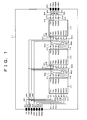
- Fig. 1 is an electrical circuit diagram in a stacked device as a semiconductor device in accordance with one embodiment of the present invention.
- Fig. 2 is a cross sectional view showing one example of a structure of the stacked device as shown in Fig. 1 and Fig. 5.
- Fig. 3 is an electrical circuit diagram in a stacked device as a semiconductor device in accordance with another embodiment of the present invention.
- Fig. 4 is a cross sectional view showing one example of a structure of the stacked device as shown in Fig. 3.
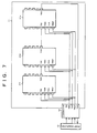
- Fig. 5 is an electrical circuit diagram in a stacked device as a semiconductor device in accordance with yet another embodiment of the present invention.
- Fig. 6 is a block diagram showing one example of a device which is compatible with the boundary scan test.
- Fig. 7 is a block diagram explaining a method of a conventional boundary scan test.
- Fig. 1 is an electrical circuit diagram in a stacked device 21, which is a semiconductor device of one embodiment of the present invention.
- a stacked device 21 which is a semiconductor device of one embodiment of the present invention.
- chips ic1, ic2, and ic3 (will be indicated by reference symbol “ic" when referring to the chips in general) which are sealed integrally.
- Each chip ic includes, in addition to a core logic 1 as shown in Fig. 6 for realizing an intended function of the device, BSR 2, instruction register 3, bypass register 4, option register 5, TAP 6 for controlling these elements, and TAPC 7 for controlling the TAP 6.
- the core logic 1 may have any arrangement.
- Pads AC, AM, and AR of each chip ic are connected, parallel to each other, via wires WC, WM, and WR, to their corresponding pins BC, BM, and BR of the stacked device 21.
- pad AO corresponding to the signal line TDO and pad AI corresponding to the signal line TDI are successively and serially connected to each other via wire WOI connecting the chips between devices of preceding and following stages, and pad AI corresponding to the signal line TDI of the chip icl of the first stage and pad AO corresponding to the signal line TDO of the chip ic3 of the last stage are connected to their corresponding pins BI and BO, respectively.
- pads A1, A2, and A3, and pads A4, A5, and A6, respectively corresponding to signal lines PAD1, PAD2, and PAD3, and signal lines PAD 4, PADS, and PAD6 for the common core logic 1 the pads A4, A5, and A6, respectively corresponding to the output signal lines PAD4, PADS, and PAD 6 of the chip of a preceding stage are connected, parallel to each other, via wires W41, W52, and W63 connecting the chips, to the pads A1, A2, and A3, respectively corresponding to the input signal lines PAD1, PAD2, and PAD 3 of the chip of the following stage, respectively.
- pads A1, A2, and A3, respectively corresponding to the input signal lines PAD1, PAD2, and PAD3 of the chip ic1 of the first stage are connected, parallel to each other, via wires W1, W2, and W3 connecting the chips, to their corresponding pins B1, B2, and B3, respectively.
- the pads A4, A5, and A6, respectively corresponding to the output signal lines PAD4, PAD5, and PAD6 of the chip ic3 of the last stage are connected, parallel to each other, via wires W4, W5, and W6, to their corresponding pins B4, B5, B6, respectively.
- the semiconductor device of the present embodiment includes a plurality of chips ic which are integrally sealed, a test signal input terminal (pin BI) for receiving an externally supplied test signal, a test result output terminal (pin BO) for outputting the test result of the plural chips ic to outside, and control signal input terminals (pins BC, BM, and BR) for receiving externally supplied test control signals.
- the test signal inputted from the test signal input terminal (pin BI) is successively transferred through the plural chips ic, whereas test control signals inputted from the control signal input terminals (pin BC, BM, and BR) are individually supplied to each chip ic.
- the stacked device 21 structured as above is mounted as the device IC1 or IC2 as shown in Fig. 7 on a substrate 11 to be subjected to a test, and TAP 6 of each chip is controlled by a host computer 13 so as to carry out the boundary scan test all at once with respect to all the chips ic in the stacked device 21. Note that, a discrete function test of each chip ic is individually carried out one after another for each chip ic using pins B1 to B6, etc.
- test commands/data input and output pins BI and BO and input pins BC, BM, and BR of signals to be used in a test of the device can be provided with the minimum required number of 4 (when omitting BR) or 5, thus carrying out the test with a smaller number of pins and reducing a test pattern length on the print substrate 11. Further, a test needs to be carried out only once.
- Fig. 2 is a cross section showing one example of a structure of the stacked device 21. Note that, even though Fig. 1 described the case of three chips ic1, ic2, and ic3, for convenience of explanation, only two chips are provided in Fig. 2.
- the stacked device 21 is a semiconductor device of a BGA structure in which two chips ic1 and ic2 are stacked on one surface of a substrate 22 and solder bump 23 is provided in a matrix on the other surface of the substrate 22.
- the chips icl and ic2 are connected to each other by a pad on the substrate 22 and wire W, and to the solder bump 23 via a pattern on the substrate 22.
- the chips icl and ic2 are integrally sealed air-tight by mold resin 24.
- two chips icl and ic2 are stacked on one surface of the substrate 22, and the chips ic1 and ic2 can be connected to each other by wire WOI, W41, W52. or W63.
- Fig. 3 is an electrical circuit diagram in a stacked device 31, which is a semiconductor device of another embodiment of the present invention.
- the stacked device 31 is analogous to the foregoing stacked device 21, and thus corresponding parts or elements are given the same reference numerals and explanations thereof are omitted here.
- the chips ic1 and ic2 each includes, in addition to the core logic 1 for realizing an intended function of the device, BSR2, instruction register 3, bypass register 4, option register 5, TAP 6 for controlling these elements, and TAPC 7 for controlling the TAP 6, along with other elements.
- pads AC, AM, and AR, respectively corresponding to signal lines TCK, TMS, and TRST are connected, parallel to each other, via wires WC, WM, and WR, to their corresponding pins BC, BM, and BR of the stacked device 31.
- pad AO corresponding to the signal line TDO is connected via wire WO to pin BO, which is individually provided for each of the chips icl and ic2, and a boundary scan test output is serially outputted therefrom.
- a pad AI corresponding to signal line TDI of the chip icl of the first stage is connected via wire W1 to its corresponding pin BI, whereas a pad AI corresponding to signal line TDI of the chip ic2 of the following stage is connected via wire WOI to pin BO which corresponds to signal line TDO of the chip ic1 of the preceding stage.
- pads A1, A2, and A3, and pads A4, A5, and A6, respectively corresponding to the signal lines PAD1, PAD2, and PAD3 and signal lines PAD4, PADS, and PAD6 for the common core logic 1 of each chip ic are connected, parallel to each other, via wires W1, W2, and W3, and wires W4, W5, and W6, to the pins B1, B2, and B3 and pins B4, B5, and B6, respectively, which are separately provided.
- test commands/data output pin BO of the device for each of the chips ic1 and ic2, to provide the other test commands/data input pin BI and input pins BC, BM, and BR of signals to be used in a test with the minimum required number of 3 (when omitting BR) or 4, thus carrying out the test with a smaller number of pins and reducing a test pattern length on the print substrate 11. Further, the test needs to be carried out only once.
- Fig. 4 is a cross section showing one example of a structure of the stacked device 31.
- the stacked device 31 is a semiconductor device of a DIL (Dual In Line) structure in which chips icl and ic2 are stuck on the front and back surfaces of a substrate 32, respectively, and pins 33 are disposed in a row from the both ends of the pair of the chips ic1 and ic2. Due to this structure, unlike the foregoing structure, the chips icl and ic2, respectively on the front and back surfaces of the substrate 32, cannot be connected to each other by wire, and thus the chips ic1 and ic2 are connected to each other via test commands/data output pin BO. Also, the chips icl and ic2 are integrally sealed air-tight by mold resin 24.
- DIL Direct In Line
- Fig. 5 is an electrical circuit diagram in a stacked device 41, which is a semiconductor device of yet another embodiment of the present invention.
- the stacked device 41 is analogous to the foregoing stacked devices 21 and 31, and corresponding parts or elements will be given the same reference numerals and explanations thereof are omitted here.
- the chips icla, ic2a, and ic3a of the stacked device 41 are the same as the foregoing chips ic1, ic2, and ic3 in the structure where the BSR2 and TAP 6 are provided for each chip in addition to the core logic 1 for realizing an intended function of the device, as shown in Fig. 6, yet they are different with regard to TAPC 7, instruction register 3, bypass register 4, and option register 5, etc., which are not provided on the chips ic2a and ic3a of the second and subsequent stages, but are provided only on the chip icla of the first stage.
- the chip icla is provided with relay signal lines TDIa and TDOa of the signal lines TDI and TDO, and output signal lines TAPO, TAP1, TAP2, TAP3, and TAP4 corresponding to the signal lines TCK, TMS, and TRST.
- the chips ic2a and ic3a are each provided with signal lines TDI and TDO, as well as signal lines TAPO, TAP1, TAP2, TAP3, and TAP4.
- Pads AI, AC, AM, and AR of the chip icla of the first stage, respectively corresponding to the signal lines TD1, TCK, TMS, and TRST are connected, parallel to each other, via wires WI, WC, WM, and WR, to their corresponding pins BI, BC, BM, and BR of the stacked device 41.
- Pad AOa which corresponds to the relay signal line TDOa is connected to pin BO via wire WO.
- pads C0, C1, C2, C3, and C4, respectively corresponding to signal lines TAP0, TAP1, TAP2, TAP3, and TAP4 are connected, parallel to each other, via wires W10, W11, W12, W13, and W14, to their corresponding pads C0, C1, C2, C3, and C4 of the signal lines TAP0, TAP1, TAP2, TAP3, and TAP4 of the chips ic2a and ic3a, respectively.
- pad AO corresponding to signal line TDO is connected, via wire WOI connecting the chips, to pad AI which corresponds to signal line TDI of the chip ic2a
- pad AO corresponding to signal line TDO of the chip ic2a is connected, via wire WOI connecting the chips, to pad AI which corresponds to signal line TDI of the chip ic3a
- pad AO corresponding to signal line TDO of the chip ic3a is connected, via wire WOI connecting the chips, to pad AIa which corresponds to signal line TDIa of the chip icla.
- pads A1, A2, and A3 and pads A4, A5, and A6, respectively corresponding to the signal lines PAD1, PAD2, and PAD3 and signal lines PAD4, PADS, and PAD6 for the common core logic 1 of each chip ic are connected, parallel to each other, via wires W1, W2, and W3 and wires W4, W5, and W6, to the pins B1, B2, and B3 and pins B4, B5, and B6, respectively, which are separately provided.
- the semiconductor device of the present embodiment includes a plurality of chips which are integrally sealed, test signal input terminal (pin BI) for receiving an externally supplied test signal, test result output terminal (pin BO) for outputting the test result of the plural chips ic to outside, and control signal input terminals (pins BC, BM, and BR) for receiving externally supplied test control signals.
- test signal input terminal pin BI
- test result output terminal pin BO
- control signal input terminals pins BC, BM, and BR
- test signal is inputted to the chip icla, and successively transferred through the other chips, and after being inputted again into the chip icla, outputted as a test result to outside. Meanwhile, the test control signals are individually supplied to the other chips from the chip icla.
- the TAP6 of each chip ic is controlled by way of TAPC 7 of the chip icla by the host computer 13 as shown in Fig. 7 so as to perform the boundary scan test all at once with respect to all the chips ic in the stacked device 41.
- test commands/data input and output pins BI and BO and input pins BC, BM, and BR of signals to be used in a test of the device can be provided with the minimum required number of 4 (when omitting BR) or 5, thus carrying out the test with a smaller number of pins and reducing a test pattern length on the print substrate 11. Further, the test needs to be carried out only once.
- the number of gates of the chips ic2a and ic3a can be reduced, thereby reducing the chip area and the number of manufacturing steps.
- the number of gates a single TAPC possesses is equivalent to twenty to thirty BSRs, and thus the number of gates reduced in each of the chips ic2a and ic3a is equivalent to twenty to thirty BSRs.
- the chips are connected to each other, and thus the structure thereof is, for example, as shown in Fig. 2, as with the stacked device 21.
- the semiconductor device of the present invention in which a plurality of semiconductor integrated circuit chips are integrally sealed, may have an arrangement including: a test register provided for each of input and output terminals of a core logic of each chip; and a control circuit for controlling the test register for testing the chip, test commands/data input and output terminals connected to the control circuit, and input terminals of signals to be used in the test, which are all mounted on each chip, a test commands/data input terminal of a device being connected to the test commands/data input terminal of a chip of a first stage, and the test commands/data output terminal of a chip of a preceding stage being serially connected to the test commands/data input terminal of a chip of a following stage, and the test commands/data output terminal of a chip of a last stage being connected to a test commands/data output terminal of the device, and input terminals of the device for the signals to be used in the test being connected to the corresponding input terminals of each chip for the signals to be used in the test.
- each chip in testing, for example, by the boundary scan test, a semiconductor device in which a plurality of semiconductor integrated circuit chips are integrally sealed, each chip would mount a test register such as a BSR of a boundary scan test compatible chip, and a control circuit such as TAPC, in addition to test commands/data input and output terminals such as TDI and TDO, and input terminals of signals to be used in the test, such as TCK, TMS, and TRST.
- a test register such as a BSR of a boundary scan test compatible chip
- TAPC control circuit
- test commands/data input terminal of the device is connected to the test commands/data input terminal of the chip of the first stage, and the test commands/data output terminal of the chip of the last stage is connected to the test commands/data output terminal of the device, and the test commands/data output terminal and test commands/data input terminal are serially connected between chips of preceding and following stages within the device, utilizing the connections between the chips, and the input terminal of the device for the signal to be used in the test is connected to the corresponding input terminal of the signal of each chip.
- test commands/data input and output terminals and input terminals of a signal to be used in the test of the device can be provided with the minimum required number of 4 or 5, for example, when responding to the boundary scan test, thus carrying out the test with a smaller number of pins and reducing a test pattern length on the substrate. Further, the test needs to be carried out only once.
- the semiconductor device of the present invention in which a plurality of chips are integrally sealed, may have an arrangement including: a test register provided for each of input and output terminals of a core logic of each chip; and a control circuit for controlling the test register for testing the chip, test commands/data input and output terminals connected to the control circuit, and input terminals of signals, connected to the control circuit, to be used in the test, which are all mounted on each chip, a test commands/data input terminal of a device being connected to the test commands/data input terminal of a chip of a first stage, and the test commands/data output terminal of each chip being connected to a corresponding output terminal of the device and serially to the test commands/data input terminal of a chip of a following stage via the output terminal of the device, and input terminals of the device for the signals to be used in the test being connected to the corresponding input terminals of each chip for the signals to be used in the test.
- each chip in testing, for example, by the boundary scan test, a semiconductor device in which a plurality of semiconductor integrated circuit chips are integrally sealed, each chip would mount a test register such as a BSR of a boundary scan test compatible chip, and a control circuit such as TAPC, in addition to test commands/data input and output terminals such as TDI and TDO, and input terminals of signals to be used in the test, such as TCK, TMS, and TRST.
- a test register such as a BSR of a boundary scan test compatible chip
- TAPC control circuit
- test commands/data input terminal of the device is connected to the test commands/data input terminal of the chip of the first stage, and the test commands/data output terminal of each chip is connected to the test commands/data output terminal of the device, and due to the structure which prevents a direct connection between the chips, the test commands/data output terminal and test commands/data input terminal are serially connected to each other between the chips of preceding and following stages, and the input terminal of the device for a signal to be used in the test is connected to the corresponding input terminal of the signal of each chip.
- the test commands/data output terminal of the device needs to be provided for the number of chips provided in cases where the chips cannot be directly connected to each other
- the test commands/data input terminal and input terminal of a signal to be used in the test of the device can be provided with the minimum required number of 3 or 4, for example, when responding to the boundary scan test, thus carrying out the test with a smaller number of pins and reducing a test pattern length on the substrate. Further, the test needs to be carried out only once.
- the semiconductor device of the present invention in which a plurality of semiconductor integrated circuit chips are integrally sealed, may have an arrangement including: a test register provided for each of input and output terminals of a core logic of each chip; and a control circuit for controlling the test register for testing the chip, test commands/data relay input and output terminals connected to the control circuit, and output terminals of signals to be used in the test outputted from the control circuit, which are all mounted on a chip of a first stage, test commands/data input and output terminals of a device being respectively connected to the test commands/data input and output terminals of the chip of the first stage, and the relay output terminal of the chip of the first stage being connected to a test commands/data input terminal of a chip of a following stage, and a test commands/data output terminal and a test commands/data input terminal being serially and successively connected between chips of a preceding stage and a following stage, and a test commands/data output terminal of a chip of a last stage being connected to the relay input terminal of the chip of the
- each chip would mount a test register such as a BSR of a boundary scan test compatible chip, in addition to test commands/data input and output terminals such as TDI and TDO, and input terminals of signals to be used in the test, such as TCK, TMS, and TRST.
- a test register such as a BSR of a boundary scan test compatible chip
- test commands/data input and output terminals such as TDI and TDO
- input terminals of signals to be used in the test such as TCK, TMS, and TRST.
- the control circuit such as TAPC is mounted only on the chip of the first stage. Accordingly, the chip of the first stage would mount test commands/data relay input and output terminals and output terminals of test signals outputted from the control circuit, and the test signal is distributed from the chip of the first stage to the other chip, using the connections between the chips.
- the relay output terminal of the chip of the first stage is connected to the test commands/data input terminal of the chip of the following stage using the connection between the chips, and the test commands/data output terminal and test commands/data input terminal are serially connected to each other between the chips of preceding and following stages, and the test commands/data output terminal of the chip of the last stage is connected to the relay input terminal of the chip of the first stage so as to form a loop, thereby supplying the test commands and data to each chip.
- the test commands/data input and output terminals and input terminal of a signal to be used in the test of the device can be provided with the minimum required number of 4 or 5, for example, when responding to the boundary scan test, thus carrying out the test with a smaller number of pins and reducing a test pattern length on the substrate. Further, the test needs to be carried out only once. Further, the control circuit which is common to the plurality of chips only needs to be provided on the chip of the first stage, thus reducing the number of the other chips and in turn chip area, as well as the number of manufacturing steps.
Landscapes
- Engineering & Computer Science (AREA)
- General Engineering & Computer Science (AREA)
- Physics & Mathematics (AREA)
- General Physics & Mathematics (AREA)
- Tests Of Electronic Circuits (AREA)
- Semiconductor Integrated Circuits (AREA)
- Testing Or Measuring Of Semiconductors Or The Like (AREA)
Abstract
Description
Claims (7)
- A semiconductor device, comprising:a plurality of chips (ic), which are integrally sealed;a test signal input terminal (BI) for receiving an externally supplied test signal;a test result output terminal (BO) for outputting a test result of said plurality of chips (ic) to outside; andcontrol signal input terminals (BC, BM, BR) for receiving externally supplied test control signals,the test signal inputted from said test signal input terminal (BI) being successively transferred through said plurality of chips (ic), andthe test control signals inputted from said control signal input terminals (BC, BM, BR) being individually supplied to each of said plurality of chips (ic).
- The semiconductor device as set forth in claim 1, wherein said plurality of chips (ic) are connected to each other via said test result output terminal (BO).
- A semiconductor device, comprising:a plurality of chips (ic), which are integrally sealed;a test signal input terminal (BI) for receiving an externally supplied test signal;a test result output terminal (BO) for outputting a test result of said plurality of chips (ic) to outside; andcontrol signal input terminals (BC, BM, BR) for receiving externally supplied test control signals,only one (ic1a) of said plurality of chips (ic) being connected to said test signal input terminal (BI), to said test result output terminal (BO), and to said control signal input terminals (BC, BM, BR),the test signal being inputted to the one (ic1a) of said plurality of chips (ic) and successively transferred through the other chips, and after being inputted again into the one (ic1a) of said plurality of chips (ic), outputted as the test result to outside, andthe test control signals being individually supplied from the one (ic1a) of said plurality of chips (ic) to each of the other chips.
- The semiconductor device as set forth in claim 3, wherein only the one (ic1a) of said plurality of chips (ic) includes a controller (7) for controlling an input/output interface (6) of the test signal.
- A semiconductor device in which a plurality of chips (ic) are integrally sealed, comprising:a test register (2) provided between a core logic (1) and each of input and output terminals (8) of each chip (ic); anda control circuit (7) for controlling said test register (2) for testing the chip (ic), test commands/data input and output terminals (AI, AO) connected to said control circuit (7), and input terminals (AC, AM, AR) of signals to be used in the test, which are all mounted on each chip (ic),a test commands/data input terminal (BI) of a device being connected to the test commands/data input terminal (AI) of a chip (ic1) of a first stage, and the test commands/data output terminal (AO) of a chip of a preceding stage being serially connected to the test commands/data input terminal (AI) of a chip of a following stage, and the test commands/data output terminal (AO) of a chip (ic3) of a last stage being connected to a test commands/data output terminal (BO) of the device, and input terminals (BC, BM, BR) of the device for the signals to be used in the test being connected to the corresponding input terminals (AC, AM, AR) of the signals of each chip (ic).
- A semiconductor device in which a plurality of chips (ic) are integrally sealed, comprising:a test register (2) provided between a core logic (1) and each of input and output terminals (8) of each chip (ic); anda control circuit (7) for controlling said test register (2) for testing the chip (ic), test commands/data input and output terminals (AI, AO) connected to said control circuit (7), and input terminals (AC, AM, AR) of signals, connected to said control circuit (7), to be used in the test, which are all mounted on each chip (ic),a test commands/data input terminal (BI) of a device being connected to the test commands/data input terminal (AI) of a chip (ic1) of a first stage, and the test commands/data output terminal (AO) of each chip (ic) being connected to a corresponding output terminal (BO) of the device and serially to the test commands/data input terminal (AI) of a chip (ic) of a following stage via the output terminal (BO) of the device, and input terminals (BC, BM, BR) of the device for the signals to be used in the test being connected to the corresponding input terminals (AC, AM, AR) of the signals of each chip (ic) .
- A semiconductor device in which a plurality of chips (ic) are integrally sealed, comprising:a test register (2) provided between a core logic (1) and each of input and output terminals (8) of each chip (ic); anda control circuit (7) for controlling the test register (2) for testing the chip (ic) , test commands/data relay input and output terminals (AIa, AO) connected to said control circuit (7), and output terminals (C0-4) of signals to be used in the test outputted from the control circuit (7), which are all mounted on a chip (icla) of a first stage,test commands/data input and output terminals (BI, BO) of a device being respectively connected to the test commands/data input and output terminals (AI, AO) of the chip (ic1a) of the first stage, and the relay output terminal (AO) of the chip (ic1a) of the first stage being connected to a test commands/data input terminal (AI) of a chip (ic) of a following stage, and a test commands/data output terminal (AO) and a test commands/data input terminal (AI) being serially and successively connected between chips (ic) of preceding and following stages, and a test commands/data output terminal (AO) of a chip (ic3a) of a last stage being connected to the relay input terminal (AIa) of the chip (ic1a) of the first stage so as to form a loop, and the output terminals (C0-4) of the chip (ic1a) of the first stage for the signals to be used in the test being connected to input terminals (C0-4) of the signals of the other chips (ic).
Applications Claiming Priority (2)
| Application Number | Priority Date | Filing Date | Title |
|---|---|---|---|
| JP31848599A JP3763385B2 (en) | 1999-11-09 | 1999-11-09 | Semiconductor device |
| JP31848599 | 1999-11-09 |
Publications (3)
| Publication Number | Publication Date |
|---|---|
| EP1099953A2 true EP1099953A2 (en) | 2001-05-16 |
| EP1099953A3 EP1099953A3 (en) | 2001-05-23 |
| EP1099953B1 EP1099953B1 (en) | 2006-08-30 |
Family
ID=18099655
Family Applications (1)
| Application Number | Title | Priority Date | Filing Date |
|---|---|---|---|
| EP00305720A Expired - Lifetime EP1099953B1 (en) | 1999-11-09 | 2000-07-06 | Semiconductor device with testing capability |
Country Status (6)
| Country | Link |
|---|---|
| US (1) | US7036058B1 (en) |
| EP (1) | EP1099953B1 (en) |
| JP (1) | JP3763385B2 (en) |
| KR (1) | KR100392300B1 (en) |
| DE (1) | DE60030391T2 (en) |
| TW (1) | TW472154B (en) |
Cited By (2)
| Publication number | Priority date | Publication date | Assignee | Title |
|---|---|---|---|---|
| CN100427964C (en) * | 2003-08-04 | 2008-10-22 | 华为技术有限公司 | A Boundary Scan Test Method for Circuit Board |
| US7467341B2 (en) | 2003-02-12 | 2008-12-16 | Sharp Kabushiki Kaisha | Boundary scan controller, semiconductor apparatus, semiconductor-circuit-chip identification method for semiconductor apparatus, and semiconductor-circuit-chip control method for semiconductor apparatus |
Families Citing this family (10)
| Publication number | Priority date | Publication date | Assignee | Title |
|---|---|---|---|---|
| EP1544631B1 (en) * | 2003-12-17 | 2007-06-20 | STMicroelectronics Limited | Reset mode for scan test modes |
| EP1706752B1 (en) * | 2004-01-13 | 2008-05-07 | Nxp B.V. | Jtag test architecture for multi-chip pack |
| JP4525125B2 (en) * | 2004-03-24 | 2010-08-18 | ソニー株式会社 | Multi-chip type semiconductor device |
| KR100630716B1 (en) | 2004-11-11 | 2006-10-02 | 삼성전자주식회사 | Semiconductor memory device that can write various pattern data and its electrical test method |
| US7650542B2 (en) * | 2004-12-16 | 2010-01-19 | Broadcom Corporation | Method and system of using a single EJTAG interface for multiple tap controllers |
| KR100850208B1 (en) | 2007-01-09 | 2008-08-04 | 삼성전자주식회사 | Parallel Bit Test apparatus and Parallel Bit Test method |
| US8621301B2 (en) * | 2009-03-04 | 2013-12-31 | Alcatel Lucent | Method and apparatus for virtual in-circuit emulation |
| KR102566994B1 (en) | 2015-12-14 | 2023-08-14 | 삼성전자주식회사 | Method for performing multi-chip debugging and multi-chip system adopting the same |
| US11199582B2 (en) * | 2020-04-06 | 2021-12-14 | Xilinx, Inc. | Implementing a JTAG device chain in multi-die integrated circuit |
| CN114597195B (en) * | 2022-03-02 | 2026-04-24 | 上海壁仞科技股份有限公司 | Multi-chip systems and their operation methods |
Family Cites Families (17)
| Publication number | Priority date | Publication date | Assignee | Title |
|---|---|---|---|---|
| JPS55111151A (en) | 1979-02-20 | 1980-08-27 | Nec Corp | Integrated circuit device |
| JP2874248B2 (en) | 1990-02-26 | 1999-03-24 | 日本電気株式会社 | Electronic circuit with scan path for diagnostics |
| JP2627464B2 (en) | 1990-03-29 | 1997-07-09 | 三菱電機株式会社 | Integrated circuit device |
| US5068886A (en) * | 1990-06-28 | 1991-11-26 | Monica Lavia | Catheter or cannula position indicator for use in hemodynamic monitoring and the like |
| JPH05322988A (en) | 1992-05-18 | 1993-12-07 | Sony Corp | Inspection method for electronic device |
| US5627842A (en) * | 1993-01-21 | 1997-05-06 | Digital Equipment Corporation | Architecture for system-wide standardized intra-module and inter-module fault testing |
| US5621740A (en) * | 1993-05-14 | 1997-04-15 | Matsushita Electric Industrial Co., Ltd. | Output pad circuit for detecting short faults in integrated circuits |
| US6006343A (en) * | 1993-07-30 | 1999-12-21 | Texas Instruments Incorporated | Method and apparatus for streamlined testing of electrical circuits |
| JP3479653B2 (en) * | 1993-10-15 | 2003-12-15 | コーニンクレッカ フィリップス エレクトロニクス エヌ ヴィ | Test equipment |
| US5448525A (en) * | 1994-03-10 | 1995-09-05 | Intel Corporation | Apparatus for configuring a subset of an integrated circuit having boundary scan circuitry connected in series and a method thereof |
| US6058602A (en) * | 1998-09-21 | 2000-05-09 | Integrated Packaging Assembly Corporation | Method for encapsulating IC packages with diamond substrate |
| JPH09186418A (en) | 1995-12-28 | 1997-07-15 | Oki Electric Ind Co Ltd | Connecting structure of printed circuit board for boundary scan test |
| US5808877A (en) * | 1996-09-19 | 1998-09-15 | Samsung Electronics Co., Ltd. | Multichip package having exposed common pads |
| US6260165B1 (en) * | 1996-10-18 | 2001-07-10 | Texas Instruments Incorporated | Accelerating scan test by re-using response data as stimulus data |
| US6199182B1 (en) * | 1997-03-27 | 2001-03-06 | Texas Instruments Incorporated | Probeless testing of pad buffers on wafer |
| US6000051A (en) * | 1997-10-10 | 1999-12-07 | Logic Vision, Inc. | Method and apparatus for high-speed interconnect testing |
| US6163867A (en) * | 1998-08-28 | 2000-12-19 | Hewlett-Packard Company | Input-output pad testing using bi-directional pads |
-
1999
- 1999-11-09 JP JP31848599A patent/JP3763385B2/en not_active Expired - Fee Related
-
2000
- 2000-07-06 DE DE60030391T patent/DE60030391T2/en not_active Expired - Lifetime
- 2000-07-06 EP EP00305720A patent/EP1099953B1/en not_active Expired - Lifetime
- 2000-07-06 TW TW089113402A patent/TW472154B/en not_active IP Right Cessation
- 2000-07-13 KR KR10-2000-0040162A patent/KR100392300B1/en not_active Expired - Fee Related
- 2000-07-13 US US09/615,956 patent/US7036058B1/en not_active Expired - Fee Related
Cited By (2)
| Publication number | Priority date | Publication date | Assignee | Title |
|---|---|---|---|---|
| US7467341B2 (en) | 2003-02-12 | 2008-12-16 | Sharp Kabushiki Kaisha | Boundary scan controller, semiconductor apparatus, semiconductor-circuit-chip identification method for semiconductor apparatus, and semiconductor-circuit-chip control method for semiconductor apparatus |
| CN100427964C (en) * | 2003-08-04 | 2008-10-22 | 华为技术有限公司 | A Boundary Scan Test Method for Circuit Board |
Also Published As
| Publication number | Publication date |
|---|---|
| JP2001135786A (en) | 2001-05-18 |
| JP3763385B2 (en) | 2006-04-05 |
| TW472154B (en) | 2002-01-11 |
| EP1099953B1 (en) | 2006-08-30 |
| DE60030391T2 (en) | 2007-08-30 |
| KR100392300B1 (en) | 2003-07-22 |
| EP1099953A3 (en) | 2001-05-23 |
| US7036058B1 (en) | 2006-04-25 |
| DE60030391D1 (en) | 2006-10-12 |
| KR20010049778A (en) | 2001-06-15 |
Similar Documents
| Publication | Publication Date | Title |
|---|---|---|
| KR0174334B1 (en) | Multichip module with integrated test circuit disposed inside interposer board and manufacturing method thereof | |
| US6727723B2 (en) | Test system and manufacturing of semiconductor device | |
| US4812678A (en) | Easily testable semiconductor LSI device | |
| TWI447408B (en) | Test interposer having active circuit component and method therefor | |
| US6734549B2 (en) | Semiconductor device having a device for testing the semiconductor | |
| US11526644B2 (en) | Controlling test networks of chips using integrated processors | |
| EP2341356B1 (en) | Method and device for measuring inter-chip signals | |
| US7808092B2 (en) | Semiconductor device with a plurality of ground planes | |
| US4967142A (en) | Electronic module comprising a first substrate element with a functional part, and a second substrate element for testing an interconnection function, socket, substrate element and electronic apparatus therefor | |
| US6218202B1 (en) | Semiconductor device testing and burn-in methodology | |
| EP1099953B1 (en) | Semiconductor device with testing capability | |
| EP1498949A2 (en) | Module with tailored interconnections between integrated circuit chips | |
| US5805865A (en) | Semiconductor device | |
| US20210333326A1 (en) | Switch-Mode Based Interposer Enabling Self-Testing Of An MCM Without Known Good Die | |
| KR100687687B1 (en) | Multichip Module Packaging Method | |
| CN1996035B (en) | Device with programmable scan chains for multi-chip modules | |
| US7071719B2 (en) | Semiconductor device | |
| JP3566157B2 (en) | Semiconductor device and manufacturing method thereof | |
| Maly et al. | Multi-Chip Module Smart Substrate System | |
| JPH11218560A (en) | Inspection circuit | |
| JP2000243914A (en) | Semiconductor device | |
| Sasidhar et al. | Low cost test of MCMs using testable die carriers |
Legal Events
| Date | Code | Title | Description |
|---|---|---|---|
| PUAI | Public reference made under article 153(3) epc to a published international application that has entered the european phase |
Free format text: ORIGINAL CODE: 0009012 |
|
| PUAL | Search report despatched |
Free format text: ORIGINAL CODE: 0009013 |
|
| AK | Designated contracting states |
Kind code of ref document: A2 Designated state(s): DE FR GB NL |
|
| AX | Request for extension of the european patent |
Free format text: AL;LT;LV;MK;RO;SI |
|
| AK | Designated contracting states |
Kind code of ref document: A3 Designated state(s): AT BE CH CY DE DK ES FI FR GB GR IE IT LI LU MC NL PT SE |
|
| AX | Request for extension of the european patent |
Free format text: AL;LT;LV;MK;RO;SI |
|
| 17P | Request for examination filed |
Effective date: 20010606 |
|
| AKX | Designation fees paid |
Free format text: DE FR GB NL |
|
| 17Q | First examination report despatched |
Effective date: 20040422 |
|
| GRAP | Despatch of communication of intention to grant a patent |
Free format text: ORIGINAL CODE: EPIDOSNIGR1 |
|
| GRAS | Grant fee paid |
Free format text: ORIGINAL CODE: EPIDOSNIGR3 |
|
| RIN1 | Information on inventor provided before grant (corrected) |
Inventor name: YAMASHITA, TOSHIFUMI Inventor name: MIYACHI, KUMI |
|
| GRAA | (expected) grant |
Free format text: ORIGINAL CODE: 0009210 |
|
| AK | Designated contracting states |
Kind code of ref document: B1 Designated state(s): DE FR GB NL |
|
| REG | Reference to a national code |
Ref country code: GB Ref legal event code: FG4D |
|
| REF | Corresponds to: |
Ref document number: 60030391 Country of ref document: DE Date of ref document: 20061012 Kind code of ref document: P |
|
| ET | Fr: translation filed | ||
| PLBE | No opposition filed within time limit |
Free format text: ORIGINAL CODE: 0009261 |
|
| STAA | Information on the status of an ep patent application or granted ep patent |
Free format text: STATUS: NO OPPOSITION FILED WITHIN TIME LIMIT |
|
| 26N | No opposition filed |
Effective date: 20070531 |
|
| PGFP | Annual fee paid to national office [announced via postgrant information from national office to epo] |
Ref country code: NL Payment date: 20100716 Year of fee payment: 11 |
|
| PGFP | Annual fee paid to national office [announced via postgrant information from national office to epo] |
Ref country code: DE Payment date: 20100630 Year of fee payment: 11 Ref country code: FR Payment date: 20100805 Year of fee payment: 11 Ref country code: GB Payment date: 20100630 Year of fee payment: 11 |
|
| REG | Reference to a national code |
Ref country code: NL Ref legal event code: V1 Effective date: 20120201 |
|
| GBPC | Gb: european patent ceased through non-payment of renewal fee |
Effective date: 20110706 |
|
| REG | Reference to a national code |
Ref country code: FR Ref legal event code: ST Effective date: 20120330 |
|
| PG25 | Lapsed in a contracting state [announced via postgrant information from national office to epo] |
Ref country code: DE Free format text: LAPSE BECAUSE OF NON-PAYMENT OF DUE FEES Effective date: 20120201 Ref country code: FR Free format text: LAPSE BECAUSE OF NON-PAYMENT OF DUE FEES Effective date: 20110801 |
|
| REG | Reference to a national code |
Ref country code: DE Ref legal event code: R119 Ref document number: 60030391 Country of ref document: DE Effective date: 20120201 |
|
| PG25 | Lapsed in a contracting state [announced via postgrant information from national office to epo] |
Ref country code: NL Free format text: LAPSE BECAUSE OF NON-PAYMENT OF DUE FEES Effective date: 20120201 |
|
| PG25 | Lapsed in a contracting state [announced via postgrant information from national office to epo] |
Ref country code: GB Free format text: LAPSE BECAUSE OF NON-PAYMENT OF DUE FEES Effective date: 20110706 |