EP1099151B1 - A system to reduce power consumption - Google Patents
A system to reduce power consumption Download PDFInfo
- Publication number
- EP1099151B1 EP1099151B1 EP00930452A EP00930452A EP1099151B1 EP 1099151 B1 EP1099151 B1 EP 1099151B1 EP 00930452 A EP00930452 A EP 00930452A EP 00930452 A EP00930452 A EP 00930452A EP 1099151 B1 EP1099151 B1 EP 1099151B1
- Authority
- EP
- European Patent Office
- Prior art keywords
- arm
- coprocessor
- power reduction
- instruction
- register
- Prior art date
- Legal status (The legal status is an assumption and is not a legal conclusion. Google has not performed a legal analysis and makes no representation as to the accuracy of the status listed.)
- Expired - Lifetime
Links
Images


Classifications
-
- G—PHYSICS
- G06—COMPUTING; CALCULATING OR COUNTING
- G06F—ELECTRIC DIGITAL DATA PROCESSING
- G06F9/00—Arrangements for program control, e.g. control units
- G06F9/06—Arrangements for program control, e.g. control units using stored programs, i.e. using an internal store of processing equipment to receive or retain programs
- G06F9/30—Arrangements for executing machine instructions, e.g. instruction decode
- G06F9/30181—Instruction operation extension or modification
- G06F9/30189—Instruction operation extension or modification according to execution mode, e.g. mode flag
-
- G—PHYSICS
- G06—COMPUTING; CALCULATING OR COUNTING
- G06F—ELECTRIC DIGITAL DATA PROCESSING
- G06F1/00—Details not covered by groups G06F3/00 - G06F13/00 and G06F21/00
- G06F1/26—Power supply means, e.g. regulation thereof
- G06F1/32—Means for saving power
- G06F1/3203—Power management, i.e. event-based initiation of a power-saving mode
- G06F1/3234—Power saving characterised by the action undertaken
- G06F1/3237—Power saving characterised by the action undertaken by disabling clock generation or distribution
-
- G—PHYSICS
- G06—COMPUTING; CALCULATING OR COUNTING
- G06F—ELECTRIC DIGITAL DATA PROCESSING
- G06F1/00—Details not covered by groups G06F3/00 - G06F13/00 and G06F21/00
- G06F1/26—Power supply means, e.g. regulation thereof
- G06F1/32—Means for saving power
- G06F1/3203—Power management, i.e. event-based initiation of a power-saving mode
- G06F1/3234—Power saving characterised by the action undertaken
- G06F1/3287—Power saving characterised by the action undertaken by switching off individual functional units in the computer system
-
- G—PHYSICS
- G06—COMPUTING; CALCULATING OR COUNTING
- G06F—ELECTRIC DIGITAL DATA PROCESSING
- G06F9/00—Arrangements for program control, e.g. control units
- G06F9/06—Arrangements for program control, e.g. control units using stored programs, i.e. using an internal store of processing equipment to receive or retain programs
- G06F9/30—Arrangements for executing machine instructions, e.g. instruction decode
- G06F9/30003—Arrangements for executing specific machine instructions
- G06F9/30076—Arrangements for executing specific machine instructions to perform miscellaneous control operations, e.g. NOP
-
- G—PHYSICS
- G06—COMPUTING; CALCULATING OR COUNTING
- G06F—ELECTRIC DIGITAL DATA PROCESSING
- G06F9/00—Arrangements for program control, e.g. control units
- G06F9/06—Arrangements for program control, e.g. control units using stored programs, i.e. using an internal store of processing equipment to receive or retain programs
- G06F9/30—Arrangements for executing machine instructions, e.g. instruction decode
- G06F9/30181—Instruction operation extension or modification
-
- G—PHYSICS
- G06—COMPUTING; CALCULATING OR COUNTING
- G06F—ELECTRIC DIGITAL DATA PROCESSING
- G06F9/00—Arrangements for program control, e.g. control units
- G06F9/06—Arrangements for program control, e.g. control units using stored programs, i.e. using an internal store of processing equipment to receive or retain programs
- G06F9/30—Arrangements for executing machine instructions, e.g. instruction decode
- G06F9/38—Concurrent instruction execution, e.g. pipeline, look ahead
- G06F9/3877—Concurrent instruction execution, e.g. pipeline, look ahead using a slave processor, e.g. coprocessor
-
- Y—GENERAL TAGGING OF NEW TECHNOLOGICAL DEVELOPMENTS; GENERAL TAGGING OF CROSS-SECTIONAL TECHNOLOGIES SPANNING OVER SEVERAL SECTIONS OF THE IPC; TECHNICAL SUBJECTS COVERED BY FORMER USPC CROSS-REFERENCE ART COLLECTIONS [XRACs] AND DIGESTS
- Y02—TECHNOLOGIES OR APPLICATIONS FOR MITIGATION OR ADAPTATION AGAINST CLIMATE CHANGE
- Y02D—CLIMATE CHANGE MITIGATION TECHNOLOGIES IN INFORMATION AND COMMUNICATION TECHNOLOGIES [ICT], I.E. INFORMATION AND COMMUNICATION TECHNOLOGIES AIMING AT THE REDUCTION OF THEIR OWN ENERGY USE
- Y02D10/00—Energy efficient computing, e.g. low power processors, power management or thermal management
Definitions
- the present invention relates to the field of computer processing systems and methods. More particularly, the present invention relates to a system and method to improve power consumption in Advanced RISC Machines (ARM) based systems by turning off certain features when operating in THUMB state.
- ARM Advanced RISC Machines
- the document ARM10 Thumb Family ARM Product Overview discloses an ARM coprocessor system.
- the ARM10TDMI integer core features the ARM 32-bit RISC instruction set, and Thumb compressed 16-bit instruction set.
- US-A-5,392,437 discloses a mechanism for powering down a functional unit on an integrated circuit having multiple functional units. Some of the functional units are clocked independently of each other. That document also shows a method and mechanism for indicating to the functional unit whether it is required for use, as well as a method and mechanism for powering down the functional unit transparent and independent of the rest of the functional units when the functional unit is not required for use.
- Computer systems and circuits have made a significant contribution towards the advancement of modem society and are utilized in a number of applications to achieve advantageous results.
- Computer systems typically include a processor that operates in accordance with a set of instructions.
- Numerous electronic technologies such as digital computers, calculators, audio devices, video equipment, and telephone systems include processors that have facilitated increased productivity and reduced costs in analyzing and communicating data, ideas and trends in most areas of business, science, education and entertainment.
- the processors designed to provide these results are Advanced RISC Machines (ARM) that operate in accordance with a reduced instruction set computer architecture (RISC).
- RISC reduced instruction set computer architecture
- ARM machines typically utilize coprocessors that consume significant power even when they are not engaged in supporting current ARM operations.
- ARM processors deliver relatively high performance and offer significant flexibility through a very powerful instruction set.
- the relative simplicity of a typical ARM processor facilitates a high instruction throughput and efficient time interrupt response from a compact and cost effective device.
- Pipelining is utilized to enable multiple components of the processing and memory systems to operate at the same time. For example, while one instruction is being executed, a subsequent instruction is being decoded, and a third instruction is fetched from memory.
- One state or instruction set includes a 32-bit ARM set and another state or instruction set includes a 16-bit THUMB set.
- the THUMB set of instructions operates on the same 32-bit registers as the ARM set of instructions and achieves approximately twice the density of the ARM set while maintaining most of the ARM set performance advantages.
- a coprocessor is usually included in a system.
- An ARM coprocessor provides additional processing power in the ARM state. Often it is advantageous to have the coprocessor executing particular instructions while a main ARM processor is performing other functions. For example a coprocessor often performs functions such as floating point operations, graphics transformations, and image compression.
- Coprocessors usually consume significant amounts of system power even though the coprocessor is not contributing to primary system operations. Reducing power consumption by components that are not contributing to the functionality of an ARM system offers many benefits. For example, power availability is often critical in wireless communication systems that utilize ARM systems to provide processing capabilities. Wireless communication systems often rely on batteries as a power supply and reducing power consumption results in longer battery life. Reducing power consumption also permits battery sizes to be reduced which permits smaller wireless communication devices to be produced. Compact wireless communication devices usually offer greater practical application utility.
- the system does not interfere with the operational functionality of the ARM system.
- Coprocessor register switching during THUMB state operations is reduced by the present invention and the present invention also facilitates the reduction of power supply requirements.
- the invention is based on the following recognitions.
- some of the coprocessor features are continuously maintained even though the coprocessor is not being utilized to process instructions or information.
- the coprocessor is not contributing to primary system operations during 16-bit THUMB transactions since a coprocessor is not used to perform 16-bit transactions.
- the THUMB instruction set is smaller than the ARM instruction set and while operating in the THUMB state the coprocessor in an ARM system is not utilized.
- the coprocessor continues to consume power even when the coprocessor is not processing instructions or information. For example the clock in the coprocessor continues to run and the coprocessor registers continue to switch state which consumes power.
- an ARM coprocessor power reduction system and method detects when an ARM system is engaging in activities that do not utilize an ARM coprocessor and turns off the ARM coprocessor clock.
- the ARM coprocessor power reduction system and method of the present invention tracks if the ARM core is engaging in ARM state or THUMB state operations.
- ARM coprocessor power reduction system and method analyzes a THUMB bit (TBIT) signal that indicates whether the ARM core is performing in an ARM state or THUMB state. If the ARM core is engaging in THUMB state operations the ARM coprocessor power reduction system and method of the present invention instructs a coprocessor clock to turn off. If the ARM core is engaging in ARM state operations the ARM coprocessor power reduction system and method of the present invention instructs a coprocessor clock to turn on.
- TBIT THUMB bit
- the present invention is an ARM coprocessor power reduction system and method that detects when an ARM system is engaging in activities that do not utilize an ARM coprocessor and turns off the ARM coprocessor clock.
- the ARM coprocessor power reduction system and method of the present invention tracks signals from the ARM core periphery to determine if the ARM core is attempting to facilitate ARM state or THUMB state operations. If the ARM coprocessor power reduction system and method of the present invention detects that the ARM core is attempting to facilitate THUMB state operations the ARM coprocessor power reduction system and method signals a clock associated with the ARM coprocessor to turn off. Since the ARM coprocessor clock is turned off the registers in the ARM coprocessor are not switching and consuming power. If the ARM coprocessor power reduction system and method of the present invention senses the ARM core is attempting to facilitate ARM state operations the ARM coprocessor power reduction system and method signals a clock associated with the ARM coprocessor to turn on.
- the ARM pipeline comprises a fetch stage, a decode stage and an execute stage.
- the ARM coprocessor power reduction system of the present invention tracks what stage a particular instruction is at in the ARM core (whether it is in fetch, decode or execute stage).
- a change in state of operation e.g., a change from ARM state to THUMB state or vice versa
- an instruction indicating the change flows though the ARM pipeline.
- the instruction is fetched, decoded and then in the execute stage the ARM core determines if the instruction is directing the ARM core to switch to a 16 bit THUMB instruction set or the 32 bit ARM instruction set.
- TBIT TSUMB Bit
- the state change instruction gets executed there are potentially two more operations to get executed pending in the pipeline, one operation in the fetch stage and one operation in the decode stage. If the operation state is changing from ARM state to THUMB state the ARM coprocessor power reduction system and method does not power off the ARM coprocessor clocks until the remaining two operations in the decode and execute stage are fully executed. Thus, if the remaining two operations in the decode stage and execute stage include ARM state operations the coprocessor has its clocks running and available to continue processing 32 bit ARM state operations.
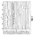
- FIG. 1 is one example of a coprocessor clock stop waveform table 100 associated with one embodiment of an ARM coprocessor power reduction system and method of the present invention.
- Coprocessor clock stop waveform table 100 illustrates when first ARM instruction 110, second ARM instruction 111 and third ARM instruction 112 and their corresponding first ARM data transfer 120, second ARM data transfer 121 and third ARM data transfer 123 are fetched, the value in a CPSTOPC register is high indicating the coprocessor clock is running.
- first THUMB instruction 113 is fetched signal AC_TBIT transitions from a logical zero (low) to a logical one (high).
- signal CP_STOPC does not switch a logical zero (instructing the coprocessor clock to continue running) to a logical one (instructing the coprocessor clock to stop running).
- Signal CP_STOPC does not transition until second THUMB instruction 114 and third THUMB instruction 116 and their associated second THUMB data transfer 124 and third THUMB data transfer 126 are complete.
- Signal CP_STOPC even senses the extended processing duration indicated by the coprocessor absent instruction 115 and its associated coprocessor absent data transaction 125 between second THUMB data transfer 124 and third THUMB data transfer 126.
- the AC_TBIT signal remains at a logical one (high) for forth THUMB instruction 117, fifth THUMB instruction 118 and forth THUMB data transfer 127.
- the TBIT signal When an ARM system is exiting the THUMB state and going to the ARM state the TBIT signal will indicate (e.g., go low) it is processing ARM state operations.
- the coprocessor clock starts during the same cycle when the ARM system is exiting the THUMB state and going to the ARM state.
- the coprocessor is available to continue processing 32 bit ARM state operations if the next instruction that gets executed is a 32 bit ATM state operation.
- FIG. 2 is one example of a coprocessor clock start waveform table 200 associated with one embodiment of an ARM coprocessor power reduction system and method of the present invention.
- Coprocessor clock stop waveform table 200 illustrates when first THUMB instruction 210, second THUMB instruction 211 and third THUMB instruction 212 and their corresponding first THUMB data transfer 220, second THUMB data transfer 221 and third THUMB data transfer 223 are fetched, the value in a CPSTOPC register is low indicating the coprocessor clock is not running.
- first ARM instruction 213 is fetched signal AC_TBIT transitions from a logical one to a logical zero.
- Signal CP_STOPC transitions from a logical one to a logical zero instructing the coprocessor clock to start running.
- the value in the CPSTOPC register transitions from a logical zero to a logical one indicating the clock started running.
- the value in the CPSTOPC register remains at a logical one for second ARM instruction 214, third ARM instruction 215, first ARM data transfer 223, second ARM data transfer 224 and third ARM data transfer 225.
- the ARM core utilizes several signals to indicate progress and advancement through the stages of the ARM coprocessor pipeline follower.
- the not memory request signal (MREQ_N or nMREQ) indicates whether a memory access is required in the next cycle. If NMREQ is low the ARM core processor requires a memory access in the next cycle.
- the not op-code fetch signal (OPC_N or nOPC) indicates whether an ARM core processor is fetching an instruction from memory. If OPC_N is low the ARM core processor is fetching an instruction from memory and if OPC_N is high data is being transferred (if there is data present).
- the not wait (WAIT_N or nWAIT) signal is utilized to cause an ARM core to wait or stall for an integer number of memory clock input (MCLK) cycles.
- MCLK is a clock that times ARM core memory accesses and internal operations.
- WAIT_N is low the ARM core waits or is stalled.
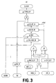
- FIG. 3 is a schematic of ARM coprocessor power reduction system 300, one embodiment of the present invention.
- ARM coprocessor power reduction system 300 comprises THUMB bit register TBIT_PF 310, wait register WAIT_N_PF 321, first logic OR component 325, not op-code fetch register OPC_N_PF 327, third logic AND component 328, second logic AND component 329, data hold register DATA_HOLD_NF 331, multiplexer MUX 332, decode register DECODE_NF 333, execute register EXECUTE_NF 334, first logic AND component 340 and stop clock register STOPCLK_NF 345.
- Registers that include a PF in their identification comprise flip flops triggered by a positive going edge of a signal and registers that include a NF in their identification comprise flip flops triggered by a negative going edge of a signal.
- TBIT_PF 310 is coupled to first logic AND component 340.
- Third logic AND component 328 is coupled to WAIT_N_PF 321, first logic OR component 325, OPC_N_PF 327, and DATA_HOLD_NF 331.
- Second logic AND component 329 is coupled to WAIT_N_PF 321, first logic OR component 325, OPC_N_PF 327, DECODE_NF 333, and EXECUTE _NF 334.
- MUX 332 is coupled to DATA_HOLD_NF 331 and DECODE_NF 333 which is coupled to EXECUTE_NF 334.
- EXECUTE_NF 334 is coupled to first logic AND component 340 which is coupled to STOPCLK_NF 345.
- First logic AND component 340 is adapted to logically analyze input signals and provide a signal that turns on or off a coprocessor clock based upon the state of instructions in an ARM pipeline. For example, first logic AND component 340 provides a signal that turns off the coprocessor clock if instructions in the ARM pipeline are THUMB state instructions and turns on the coprocessor clock if an instruction in the ARM pipeline is an ARM state instruction.
- THUMB bit register TBIT_PF 310 stores a logical value of a THUMB bit (TBIT) signal that indicates whether an instruction in an ARM pipeline is operating in a THUMB state or ARM state.
- Execute register EXECUTE_NF 334 stores information associated with an execution stage of said ARM pipeline.
- Second logic AND component 329 controls advancement of instructions and data through the ARM pipeline.
- Logic OR component 325 transmits a logical one value if an input (e.g., a not memory request signal (MREQ_N and a not op-code fetch signal OPC_N) to logic OR component 325 is a logical 1 and a logical zero if said input to logic OR component 325 is a logical zero.
- Wait register WAIT_N_PF 321 captures a value of a not wait signal (e.g., WAIT_N).
- Third logic AND component 328 transmits a signal directing stored data to be forwarded in the ARM pipeline.
- Data hold register DATA_HOLD_NF 331 stores data waiting to be processed in the ARM pipeline.
- Not op-code fetch register OPC_N_PF 327 stores the status of a not op-code fetch signal that indicates whether an ARM core processor is fetching an instruction from memory.
- Decode register DECODE_NF 333 stores information associated with a decode stage of the ARM pipeline.
- Multiplexer MUX 332 selects a signal to transmit to said decode register, such as a signal from a data hold register or from a data in signal.
- ARM instruction pipeline logic examines the information in WAIT_N_PF 321, and logical status of signals OPC_N and MREQ_N to determine when to latch instructions from an ARM system data bus through various ARM core registers. TBIT value from the previous rising edge is sampled and sent along with the data which is moving towards decode and execute stages. This enables ARM coprocessor power reduction system 300 to properly start/stop the coprocessor clock.
- FIG. 4 is an illustration of ARM coprocessor power reduction truth table 400.
- ARM coprocessor power reduction truth table 400 is the truth table for ARM coprocessor power reduction system 300.
- OPC_N signal is a logical zero
- MREQ_N signal is a logical zero at the rising edge of the clock
- the instruction remains on the ARM core data bus and no instructions are moved between DATA_HOLD_NF 331, multiplexer MUX 332, decode register DECODE_NF 333, or execute register EXECUTE _NF 334 if the value stored in WAIT_N_PF is a logical zero. No instructions are moved between DATA_HOLD_NF 331, multiplexer MUX 332, decode register DECODE_NF 333, or execute register EXECUTE_NF 334 if the value stored in register OPC_N_PF 327 is a logical one and the signal OPC_N or signal MREQ_N is a logical one.
- the ARM core does not move the current instruction through the decode stage and execute stage. However, it continues with data processing if data is present. If the information in OPC_N_PF is a logical 0, then the instruction on the ARM data bus is put in DATA_HOLD_NF 331 and is in an "on-hold" status.
- OPC_N_PF 327 If the information in OPC_N_PF 327 is a logical zero, then the instruction on the ARM data bus is put in REGISTER DECODE_NF 333 for decoding. If the value in WAIT_N_PF 321 is a logical 1 and signal OPC_N is a logical zero and signal MREQ_N is a logical zero at the falling edge of the clock, the contents of register DECODE_NF 333 flows to register EXECUTE_NF 334 for execution.
- First logic AND component 340 transmits a logical one value if its inputs, the value stored in TBIT_PF 310 and the TBIT of the value stored in EXECUTE_NF 343 are a logical one and a logical zero value if any of the inputs are a logical zero value.
- the logical values transmitted by First logic AND component 340 are temporarily stored in STOPCLK_NF 345 and then forwarded as signal CLKSTOP to the coprocessor clock. If CLKSTOP is a logical one the coprocessor clock is stopped and if CLKSTOP is a logical zero the coprocessor is started.
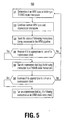
- FIG. 5 is a flow chart of ARM coprocessor power reduction method 500, one embodiment of the present invention.
- ARM coprocessor power reduction method 500 establishes if an ARM system is engaging in activities that do not utilize an ARM coprocessor and reduces power consumption by the ARM coprocessor.
- ARM coprocessor power reduction method 500 inspects signals from an ARM core periphery to determine if the ARM core is attempting to facilitate ARM state or THUMB state operations. If ARM coprocessor power reduction method 500 detects the ARM core is attempting to facilitate THUMB state operations, ARM coprocessor power reduction method 500 signals a clock associated with the ARM coprocessor to turn off.
- ARM coprocessor power reduction method 500 establishes that the series of instructions in an ARM pipeline are all THUMB state operations ARM coprocessor power reduction method 500 causes the coprocessor clock to turn off. Since the ARM coprocessor clock is turned off the registers in the ARM coprocessor are not switching and consuming power.
- ARM coprocessor power reduction method 500 determines if an ARM core is fetching a THUMB state instruction. In one embodiment, ARM coprocessor power reduction method 500 checks if the ARM processor is engaging in an instruction fetch. If an instruction is being fetched, ARM coprocessor power reduction method 500 captures the logical state of a TBIT signal associated with the instruction being fetched. For example, ARM coprocessor power reduction method 500 scans a not memory request signal (MREQ_N or nMREQ), a not op-code fetch signal (OPC_N or nOPC) and a not wait signal (WAIT_N or nWAIT) to determine if an ARM core is fetching an instruction.
- MREQ_N or nMREQ not memory request signal
- OPC_N or nOPC not op-code fetch signal
- WAIT_N or nWAIT WAIT_N or nWAIT
- a logical zero (low) TBIT signal indicates an ARM state instruction and a logical one (high) TBIT signal indicates a THUMB state instruction.
- ARM coprocessor power reduction method 500 continues normal ARM core and coprocessing procedures in Step 520 ARM.
- ARM coprocessor power reduction method 500 continues normal ARM core and coprocessing procedures by moving an instruction from the fetch stage to the decode stage and advancing the instruction on to the execution stage.
- ARM coprocessor power reduction method 500 tracks the state of following instructions being processed in the ARM pipeline.
- ARM coprocessor power reduction method 500 stores the logical value of a TBIT signal in a TBIT register (e.g., TBIT_PF 210).
- TBIT_PF 210 a TBIT register
- the TBIT value is stored when an instruction is moved from the fetch stage into the decode stage of the pipeline.
- Step 540 ARM coprocessor power reduction method 500 analyzes if it is appropriate to turn off a coprocessor clock.
- ARM coprocessor power reduction method 500 it is appropriate to turn off a coprocessor clock if ARM coprocessor power reduction method 500 establishes the instructions being processing in an ARM pipeline are THUMB state instructions or data associated with a THUMB state instruction. For example, if THUMB state instruction or data associated with the THUMB state instructions are occupying the stages of the ARM pipeline it is appropriate to turn off the coprocessor clock. If it is not appropriate to turn off a coprocessor clock ARM coprocessor power reduction method 500 loops back to step 520. If it is appropriate to turn off a coprocessor clock ARM coprocessor power reduction method 500 proceeds to step 550.
- ARM coprocessor power reduction method 500 turns off the coprocessor clock. In one embodiment of the present invention ARM coprocessor power reduction method 500 transmits a signal to the coprocessor clock to stop.
- ARM coprocessor power reduction method 500 examines if it is appropriate to turn on a coprocessor clock. In one embodiment of ARM coprocessor power reduction method 500 it is appropriate to turn on a coprocessor clock if ARM coprocessor power reduction method 500 ascertains an instruction in an ARM pipeline is an ARM state instruction or data associated with an ARM state instruction. For example, if an ARM state instruction or data associated with the ARM state instruction is occupying an ARM pipeline register it is appropriate to turn on the coprocessor clock. In one embodiment, ARM coprocessor power reduction method 500 continues to monitor a TBIT signal associated with instruction fetches after the coprocessor clock is turned off.
- ARM coprocessor power reduction method 500 interprets a TBIT value of logical zero to indicate the associated instruction fetch is an ARM state instruction fetch. If a following fetch is an ARM state instruction then it is appropriate to turn on the coprocessor clock. If it is not appropriate to turn on a coprocessor clock ARM coprocessor power reduction method 500 loops back to step 550. If it is appropriate to turn on a coprocessor clock ARM coprocessor power reduction method 500 proceeds to step 570.
- step 570 ARM coprocessor power reduction method 500 switches on a coprocessor clock and loops back to step 510.
- ARM coprocessor power reduction method 500 establishes in step 540 if an instruction being processing in an ARM pipeline are THUMB state instructions or data associated with a THUMB state instruction.
- a stored wait value e.g., WAIT_N_PF 221
- WAIT_N_PF 221 a stored wait value
- OPC_N signal and a MREQ_N signal are a logical zero
- ARM coprocessor power reduction method 500 compares the TBIT associated with an instruction in a pipeline execute register (e.g., EXECUTE_NF 234) and a stored TBIT value in a TBIT register (e.g., TBIT_PF 210).
- both the TBIT associated with an instruction in a pipeline execute register e.g., EXECUTE_NF 234
- a stored TBIT value in the TBIT register e.g., TBIT_PF_210
- ARM coprocessor power reduction method 500 stops the coprocessor clock. If either the TBIT associated with an instruction in a pipeline execute register (e.g., EXECUTE_NF 234) or a stored TBIT value in the TBIT register (e.g., TBIT_PF 210) is a logical zero, ARM coprocessor power reduction method 500 does not stop the coprocessor clock.
- the system and method of the present invention reduces power consumption by coprocessors in an ARM system.
- the system and method does not interfere with the operational functionality of the ARM system.
- Coprocessor register switching during THUMB state operations is reduced by the present invention and the present invention also facilitates the reduction of power supply requirements.
Abstract
Description
- The present invention relates to the field of computer processing systems and methods. More particularly, the present invention relates to a system and method to improve power consumption in Advanced RISC Machines (ARM) based systems by turning off certain features when operating in THUMB state.
- The document ARM10 Thumb Family ARM Product Overview discloses an ARM coprocessor system. The ARM10TDMI integer core features the ARM 32-bit RISC instruction set, and Thumb compressed 16-bit instruction set.
- US-A-5,392,437 discloses a mechanism for powering down a functional unit on an integrated circuit having multiple functional units. Some of the functional units are clocked independently of each other. That document also shows a method and mechanism for indicating to the functional unit whether it is required for use, as well as a method and mechanism for powering down the functional unit transparent and independent of the rest of the functional units when the functional unit is not required for use.
- Computer systems and circuits have made a significant contribution towards the advancement of modem society and are utilized in a number of applications to achieve advantageous results. Computer systems typically include a processor that operates in accordance with a set of instructions. Numerous electronic technologies such as digital computers, calculators, audio devices, video equipment, and telephone systems include processors that have facilitated increased productivity and reduced costs in analyzing and communicating data, ideas and trends in most areas of business, science, education and entertainment. Frequently, the processors designed to provide these results are Advanced RISC Machines (ARM) that operate in accordance with a reduced instruction set computer architecture (RISC). However, ARM machines typically utilize coprocessors that consume significant power even when they are not engaged in supporting current ARM operations.
- Typically ARM processors deliver relatively high performance and offer significant flexibility through a very powerful instruction set. The relative simplicity of a typical ARM processor facilitates a high instruction throughput and efficient time interrupt response from a compact and cost effective device. Pipelining is utilized to enable multiple components of the processing and memory systems to operate at the same time. For example, while one instruction is being executed, a subsequent instruction is being decoded, and a third instruction is fetched from memory.
- Usually an ARM processor utilizes two states or instruction sets. One state or instruction set includes a 32-bit ARM set and another state or instruction set includes a 16-bit THUMB set. The THUMB set of instructions operates on the same 32-bit registers as the ARM set of instructions and achieves approximately twice the density of the ARM set while maintaining most of the ARM set performance advantages. However, there are some instances in which more functionality and higher performance are required. In these situations a coprocessor is usually included in a system.
- An ARM coprocessor provides additional processing power in the ARM state. Often it is advantageous to have the coprocessor executing particular instructions while a main ARM processor is performing other functions. For example a coprocessor often performs functions such as floating point operations, graphics transformations, and image compression.
- Coprocessors usually consume significant amounts of system power even though the coprocessor is not contributing to primary system operations. Reducing power consumption by components that are not contributing to the functionality of an ARM system offers many benefits. For example, power availability is often critical in wireless communication systems that utilize ARM systems to provide processing capabilities. Wireless communication systems often rely on batteries as a power supply and reducing power consumption results in longer battery life. Reducing power consumption also permits battery sizes to be reduced which permits smaller wireless communication devices to be produced. Compact wireless communication devices usually offer greater practical application utility.
- It is, inter alia, an object of the invention to reduce power consumption by coprocessors in an ARM system. The invention is defined in the independent claims. Advantageous embodiments are defined in the dependent claims.
- The system does not interfere with the operational functionality of the ARM system. Coprocessor register switching during THUMB state operations is reduced by the present invention and the present invention also facilitates the reduction of power supply requirements.
- The invention is based on the following recognitions. In typical ARM systems with coprocessors, some of the coprocessor features are continuously maintained even though the coprocessor is not being utilized to process instructions or information. In particular the coprocessor is not contributing to primary system operations during 16-bit THUMB transactions since a coprocessor is not used to perform 16-bit transactions. The THUMB instruction set is smaller than the ARM instruction set and while operating in the THUMB state the coprocessor in an ARM system is not utilized. Usually the coprocessor continues to consume power even when the coprocessor is not processing instructions or information. For example the clock in the coprocessor continues to run and the coprocessor registers continue to switch state which consumes power.
- In one embodiment of the present invention, an ARM coprocessor power reduction system and method detects when an ARM system is engaging in activities that do not utilize an ARM coprocessor and turns off the ARM coprocessor clock. The ARM coprocessor power reduction system and method of the present invention tracks if the ARM core is engaging in ARM state or THUMB state operations. For example, ARM coprocessor power reduction system and method analyzes a THUMB bit (TBIT) signal that indicates whether the ARM core is performing in an ARM state or THUMB state. If the ARM core is engaging in THUMB state operations the ARM coprocessor power reduction system and method of the present invention instructs a coprocessor clock to turn off. If the ARM core is engaging in ARM state operations the ARM coprocessor power reduction system and method of the present invention instructs a coprocessor clock to turn on.
-
- Figure 1 is one example of a coprocessor clock stop waveform table associated with one embodiment of an ARM coprocessor power reduction system and method of the present invention.
- Figure 2 is one example of a coprocessor clock start waveform table associated with one embodiment of an ARM coprocessor power reduction system and method of the present invention.
- Figure 3 is a schematic of an ARM coprocessor power reduction system, one embodiment of the present invention.
- Figure 4 is an illustration of an ARM coprocessor power reduction truth table for an ARM coprocessor power reduction system of the present invention.
- Figure 5 is a flow chart of one embodiment of an ARM coprocessor power reduction method of the present invention.
- Reference will now be made in detail to the preferred embodiments of the invention, a system and method to reduce power consumption in advanced RISC machine (arm) based systems, examples of which are illustrated in the accompanying drawings. While the invention will be described in conjunction with the preferred embodiments, it will be understood that they are not intended to limit the invention to these embodiments. On the contrary, the invention is intended to cover alternatives, modifications and equivalents, which may be included within the spirit and scope of the invention as defined by the appended claims. Furthermore, in the following detailed description of the present invention, numerous specific details are set forth in order to provide a thorough understanding of the present invention. However, it will be obvious to one ordinarily skilled in the art that the present invention may be practiced without these specific details. In other instances, well known methods, procedures, components, and circuits have not been described in detail as not to unnecessarily obscure aspects of the current invention.
- The present invention is an ARM coprocessor power reduction system and method that detects when an ARM system is engaging in activities that do not utilize an ARM coprocessor and turns off the ARM coprocessor clock. For example, the ARM coprocessor power reduction system and method of the present invention tracks signals from the ARM core periphery to determine if the ARM core is attempting to facilitate ARM state or THUMB state operations. If the ARM coprocessor power reduction system and method of the present invention detects that the ARM core is attempting to facilitate THUMB state operations the ARM coprocessor power reduction system and method signals a clock associated with the ARM coprocessor to turn off. Since the ARM coprocessor clock is turned off the registers in the ARM coprocessor are not switching and consuming power. If the ARM coprocessor power reduction system and method of the present invention senses the ARM core is attempting to facilitate ARM state operations the ARM coprocessor power reduction system and method signals a clock associated with the ARM coprocessor to turn on.
- As instructions are processed by the ARM core, they are also captured by an ARM pipeline that includes three stages. The ARM pipeline comprises a fetch stage, a decode stage and an execute stage. The ARM coprocessor power reduction system of the present invention tracks what stage a particular instruction is at in the ARM core (whether it is in fetch, decode or execute stage). Whenever there is a change in state of operation (e.g., a change from ARM state to THUMB state or vice versa) an instruction indicating the change flows though the ARM pipeline. The instruction is fetched, decoded and then in the execute stage the ARM core determines if the instruction is directing the ARM core to switch to a 16 bit THUMB instruction set or the 32 bit ARM instruction set. When a state change instruction gets executed a TBIT (THUMB Bit) signal will change. For example, TBIT changes from a logical zero to a logical one when the instruction is a THUMB state instruction or from a logical one to a logical zero when the instruction is an ARM state instruction.
- Even though the state change instruction gets executed there are potentially two more operations to get executed pending in the pipeline, one operation in the fetch stage and one operation in the decode stage. If the operation state is changing from ARM state to THUMB state the ARM coprocessor power reduction system and method does not power off the ARM coprocessor clocks until the remaining two operations in the decode and execute stage are fully executed. Thus, if the remaining two operations in the decode stage and execute stage include ARM state operations the coprocessor has its clocks running and available to continue processing 32 bit ARM state operations.
- Figure 1 is one example of a coprocessor clock stop waveform table 100 associated with one embodiment of an ARM coprocessor power reduction system and method of the present invention. Coprocessor clock stop waveform table 100 illustrates when
first ARM instruction 110,second ARM instruction 111 andthird ARM instruction 112 and their corresponding first ARM data transfer 120, second ARM data transfer 121 and third ARM data transfer 123 are fetched, the value in a CPSTOPC register is high indicating the coprocessor clock is running. Whenfirst THUMB instruction 113 is fetched signal AC_TBIT transitions from a logical zero (low) to a logical one (high). However, signal CP_STOPC does not switch a logical zero (instructing the coprocessor clock to continue running) to a logical one (instructing the coprocessor clock to stop running). Signal CP_STOPC does not transition untilsecond THUMB instruction 114 andthird THUMB instruction 116 and their associated second THUMB data transfer 124 and third THUMB data transfer 126 are complete. Signal CP_STOPC even senses the extended processing duration indicated by the coprocessorabsent instruction 115 and its associated coprocessor absent data transaction 125 between second THUMB data transfer 124 and third THUMB data transfer 126. The AC_TBIT signal remains at a logical one (high) forforth THUMB instruction 117,fifth THUMB instruction 118 and forth THUMB data transfer 127. - When an ARM system is exiting the THUMB state and going to the ARM state the TBIT signal will indicate (e.g., go low) it is processing ARM state operations. The coprocessor clock starts during the same cycle when the ARM system is exiting the THUMB state and going to the ARM state. Thus, the coprocessor is available to continue processing 32 bit ARM state operations if the next instruction that gets executed is a 32 bit ATM state operation.
- Figure 2 is one example of a coprocessor clock start waveform table 200 associated with one embodiment of an ARM coprocessor power reduction system and method of the present invention. Coprocessor clock stop waveform table 200 illustrates when
first THUMB instruction 210,second THUMB instruction 211 andthird THUMB instruction 212 and their corresponding first THUMB data transfer 220, second THUMB data transfer 221 and third THUMB data transfer 223 are fetched, the value in a CPSTOPC register is low indicating the coprocessor clock is not running. Whenfirst ARM instruction 213 is fetched signal AC_TBIT transitions from a logical one to a logical zero. Signal CP_STOPC transitions from a logical one to a logical zero instructing the coprocessor clock to start running. The value in the CPSTOPC register transitions from a logical zero to a logical one indicating the clock started running. The value in the CPSTOPC register remains at a logical one forsecond ARM instruction 214,third ARM instruction 215, firstARM data transfer 223, second ARM data transfer 224 and third ARM data transfer 225. - The ARM core utilizes several signals to indicate progress and advancement through the stages of the ARM coprocessor pipeline follower. The not memory request signal (MREQ_N or nMREQ) indicates whether a memory access is required in the next cycle. If NMREQ is low the ARM core processor requires a memory access in the next cycle. The not op-code fetch signal (OPC_N or nOPC) indicates whether an ARM core processor is fetching an instruction from memory. If OPC_N is low the ARM core processor is fetching an instruction from memory and if OPC_N is high data is being transferred (if there is data present). The not wait (WAIT_N or nWAIT) signal is utilized to cause an ARM core to wait or stall for an integer number of memory clock input (MCLK) cycles. MCLK is a clock that times ARM core memory accesses and internal operations. When WAIT_N is low the ARM core waits or is stalled.
- Figure 3 is a schematic of ARM coprocessor
power reduction system 300, one embodiment of the present invention. ARM coprocessorpower reduction system 300 comprises THUMB bit registerTBIT_PF 310, waitregister WAIT_N_PF 321, first logic ORcomponent 325, not op-code fetchregister OPC_N_PF 327, third logic ANDcomponent 328, second logic ANDcomponent 329, data holdregister DATA_HOLD_NF 331,multiplexer MUX 332, decoderegister DECODE_NF 333, executeregister EXECUTE_NF 334, first logic ANDcomponent 340 and stopclock register STOPCLK_NF 345. Registers that include a PF in their identification comprise flip flops triggered by a positive going edge of a signal and registers that include a NF in their identification comprise flip flops triggered by a negative going edge of a signal.TBIT_PF 310 is coupled to first logic ANDcomponent 340. Third logic ANDcomponent 328 is coupled toWAIT_N_PF 321, first logic ORcomponent 325,OPC_N_PF 327, andDATA_HOLD_NF 331. Second logic ANDcomponent 329 is coupled toWAIT_N_PF 321, first logic ORcomponent 325,OPC_N_PF 327,DECODE_NF 333, and EXECUTE_NF 334.MUX 332 is coupled toDATA_HOLD_NF 331 andDECODE_NF 333 which is coupled toEXECUTE_NF 334.EXECUTE_NF 334 is coupled to first logic ANDcomponent 340 which is coupled toSTOPCLK_NF 345. - The components of ARM coprocessor
power reduction system 300 cooperatively operate to forward ARM instructions through an ARM pipeline and initiate a signal to turn off a coprocessor clock if the ARM pipeline is processing THUMB state instructions. First logic ANDcomponent 340 is adapted to logically analyze input signals and provide a signal that turns on or off a coprocessor clock based upon the state of instructions in an ARM pipeline. For example, first logic ANDcomponent 340 provides a signal that turns off the coprocessor clock if instructions in the ARM pipeline are THUMB state instructions and turns on the coprocessor clock if an instruction in the ARM pipeline is an ARM state instruction. THUMB bit registerTBIT_PF 310 stores a logical value of a THUMB bit (TBIT) signal that indicates whether an instruction in an ARM pipeline is operating in a THUMB state or ARM state. Executeregister EXECUTE_NF 334 stores information associated with an execution stage of said ARM pipeline. - Second logic AND
component 329 controls advancement of instructions and data through the ARM pipeline. Logic ORcomponent 325 transmits a logical one value if an input (e.g., a not memory request signal (MREQ_N and a not op-code fetch signal OPC_N) to logic ORcomponent 325 is a logical 1 and a logical zero if said input to logic ORcomponent 325 is a logical zero. Waitregister WAIT_N_PF 321 captures a value of a not wait signal (e.g., WAIT_N). - Third logic AND
component 328 transmits a signal directing stored data to be forwarded in the ARM pipeline. Data holdregister DATA_HOLD_NF 331 stores data waiting to be processed in the ARM pipeline. Not op-code fetchregister OPC_N_PF 327 stores the status of a not op-code fetch signal that indicates whether an ARM core processor is fetching an instruction from memory. Decoderegister DECODE_NF 333 stores information associated with a decode stage of the ARM pipeline.Multiplexer MUX 332 selects a signal to transmit to said decode register, such as a signal from a data hold register or from a data in signal. - ARM instruction pipeline logic examines the information in
WAIT_N_PF 321, and logical status of signals OPC_N and MREQ_N to determine when to latch instructions from an ARM system data bus through various ARM core registers. TBIT value from the previous rising edge is sampled and sent along with the data which is moving towards decode and execute stages. This enables ARM coprocessorpower reduction system 300 to properly start/stop the coprocessor clock. - Figure 4 is an illustration of ARM coprocessor power reduction truth table 400. ARM coprocessor power reduction truth table 400 is the truth table for ARM coprocessor
power reduction system 300. In one embodiment of the present invention, if the output of WAIT_N_PF is a logical one, OPC_N signal is a logical zero and MREQ_N signal is a logical zero at the rising edge of the clock, then the ARM core is fetching an instruction. The instruction itself is put on the ARM core data bus at the following falling edge of the clock. The instruction remains on the ARM core data bus and no instructions are moved betweenDATA_HOLD_NF 331,multiplexer MUX 332, decoderegister DECODE_NF 333, or execute register EXECUTE _NF 334 if the value stored in WAIT_N_PF is a logical zero. No instructions are moved betweenDATA_HOLD_NF 331,multiplexer MUX 332, decoderegister DECODE_NF 333, or executeregister EXECUTE_NF 334 if the value stored inregister OPC_N_PF 327 is a logical one and the signal OPC_N or signal MREQ_N is a logical one. If the value inWAIT_N_PF 321 is a logical one and either the OPC_N signal is a logical one or the MREQ_N signal is a logical one at the falling edge of the clock, the ARM core does not move the current instruction through the decode stage and execute stage. However, it continues with data processing if data is present. If the information in OPC_N_PF is a logical 0, then the instruction on the ARM data bus is put inDATA_HOLD_NF 331 and is in an "on-hold" status. - During the remaining states of ARM coprocessor power reduction truth table 400 instructions are moving through stages of the pipeline. If the information in
WAIT_N_PF 321 is a logical one and the OPC_N signal is a logical zero and the MREQ_N signal is a logical zero at the falling edge of the clock, the ARM core moves a current instruction to the decode stage. The status of the information inOPC_NPF 327 determines which instruction is moved to the decode stage. If the information inOPC_N_PF 327 is a logical one then the instruction inDATA_HOLD_NF 331 is moved to the decode stage because the instruction inDATA_HOLD_NF 331 didn't go through decode stage yet. If the information inOPC_N_PF 327 is a logical zero, then the instruction on the ARM data bus is put inREGISTER DECODE_NF 333 for decoding. If the value inWAIT_N_PF 321 is a logical 1 and signal OPC_N is a logical zero and signal MREQ_N is a logical zero at the falling edge of the clock, the contents ofregister DECODE_NF 333 flows to registerEXECUTE_NF 334 for execution. - First logic AND
component 340 transmits a logical one value if its inputs, the value stored inTBIT_PF 310 and the TBIT of the value stored in EXECUTE_NF 343 are a logical one and a logical zero value if any of the inputs are a logical zero value. The logical values transmitted by First logic ANDcomponent 340 are temporarily stored inSTOPCLK_NF 345 and then forwarded as signal CLKSTOP to the coprocessor clock. If CLKSTOP is a logical one the coprocessor clock is stopped and if CLKSTOP is a logical zero the coprocessor is started. - Figure 5 is a flow chart of ARM coprocessor
power reduction method 500, one embodiment of the present invention. ARM coprocessorpower reduction method 500 establishes if an ARM system is engaging in activities that do not utilize an ARM coprocessor and reduces power consumption by the ARM coprocessor. In one embodiment, ARM coprocessorpower reduction method 500 inspects signals from an ARM core periphery to determine if the ARM core is attempting to facilitate ARM state or THUMB state operations. If ARM coprocessorpower reduction method 500 detects the ARM core is attempting to facilitate THUMB state operations, ARM coprocessorpower reduction method 500 signals a clock associated with the ARM coprocessor to turn off. For example, if ARM coprocessorpower reduction method 500 establishes that the series of instructions in an ARM pipeline are all THUMB state operations ARM coprocessorpower reduction method 500 causes the coprocessor clock to turn off. Since the ARM coprocessor clock is turned off the registers in the ARM coprocessor are not switching and consuming power. - In
Step 510 ARM coprocessorpower reduction method 500 determines if an ARM core is fetching a THUMB state instruction. In one embodiment, ARM coprocessorpower reduction method 500 checks if the ARM processor is engaging in an instruction fetch. If an instruction is being fetched, ARM coprocessorpower reduction method 500 captures the logical state of a TBIT signal associated with the instruction being fetched. For example, ARM coprocessorpower reduction method 500 scans a not memory request signal (MREQ_N or nMREQ), a not op-code fetch signal (OPC_N or nOPC) and a not wait signal (WAIT_N or nWAIT) to determine if an ARM core is fetching an instruction. In one example a logical zero (low) TBIT signal indicates an ARM state instruction and a logical one (high) TBIT signal indicates a THUMB state instruction. After ARM coprocessorpower reduction method 500 determines if the ARM core is fetching a THUMB state instruction, ARM coprocessorpower reduction method 500 proceeds to Step 520 - ARM coprocessor
power reduction method 500 continues normal ARM core and coprocessing procedures inStep 520 ARM. In one example, ARM coprocessorpower reduction method 500 continues normal ARM core and coprocessing procedures by moving an instruction from the fetch stage to the decode stage and advancing the instruction on to the execution stage. - In
Step 530 ARM coprocessorpower reduction method 500 tracks the state of following instructions being processed in the ARM pipeline. In one embodiment of ARM coprocessorpower reduction method 500 stores the logical value of a TBIT signal in a TBIT register (e.g., TBIT_PF 210). In one example the TBIT value is stored when an instruction is moved from the fetch stage into the decode stage of the pipeline. - In
Step 540 ARM coprocessorpower reduction method 500 analyzes if it is appropriate to turn off a coprocessor clock. In one embodiment of ARM coprocessorpower reduction method 500 it is appropriate to turn off a coprocessor clock if ARM coprocessorpower reduction method 500 establishes the instructions being processing in an ARM pipeline are THUMB state instructions or data associated with a THUMB state instruction. For example, if THUMB state instruction or data associated with the THUMB state instructions are occupying the stages of the ARM pipeline it is appropriate to turn off the coprocessor clock. If it is not appropriate to turn off a coprocessor clock ARM coprocessorpower reduction method 500 loops back tostep 520. If it is appropriate to turn off a coprocessor clock ARM coprocessorpower reduction method 500 proceeds to step 550. - In
Step 550 ARM coprocessorpower reduction method 500 turns off the coprocessor clock. In one embodiment of the present invention ARM coprocessorpower reduction method 500 transmits a signal to the coprocessor clock to stop. - In
Step 560 ARM coprocessorpower reduction method 500 examines if it is appropriate to turn on a coprocessor clock. In one embodiment of ARM coprocessorpower reduction method 500 it is appropriate to turn on a coprocessor clock if ARM coprocessorpower reduction method 500 ascertains an instruction in an ARM pipeline is an ARM state instruction or data associated with an ARM state instruction. For example, if an ARM state instruction or data associated with the ARM state instruction is occupying an ARM pipeline register it is appropriate to turn on the coprocessor clock. In one embodiment, ARM coprocessorpower reduction method 500 continues to monitor a TBIT signal associated with instruction fetches after the coprocessor clock is turned off. For example, ARM coprocessorpower reduction method 500 interprets a TBIT value of logical zero to indicate the associated instruction fetch is an ARM state instruction fetch. If a following fetch is an ARM state instruction then it is appropriate to turn on the coprocessor clock. If it is not appropriate to turn on a coprocessor clock ARM coprocessorpower reduction method 500 loops back tostep 550. If it is appropriate to turn on a coprocessor clock ARM coprocessorpower reduction method 500 proceeds to step 570. - In
step 570, ARM coprocessorpower reduction method 500 switches on a coprocessor clock and loops back tostep 510. - As indicated above, ARM coprocessor
power reduction method 500 establishes instep 540 if an instruction being processing in an ARM pipeline are THUMB state instructions or data associated with a THUMB state instruction. In one embodiment of ARM coprocessorpower reduction method 500, if a stored wait value (e.g., WAIT_N_PF 221) is a logical one and both an OPC_N signal and a MREQ_N signal are a logical zero, ARM coprocessorpower reduction method 500 compares the TBIT associated with an instruction in a pipeline execute register (e.g., EXECUTE_NF 234) and a stored TBIT value in a TBIT register (e.g., TBIT_PF 210). If both the TBIT associated with an instruction in a pipeline execute register (e.g., EXECUTE_NF 234) and a stored TBIT value in the TBIT register (e.g., TBIT_PF_210) are a logical one ARM coprocessorpower reduction method 500 stops the coprocessor clock. If either the TBIT associated with an instruction in a pipeline execute register (e.g., EXECUTE_NF 234) or a stored TBIT value in the TBIT register (e.g., TBIT_PF 210) is a logical zero, ARM coprocessorpower reduction method 500 does not stop the coprocessor clock. - Thus, the system and method of the present invention reduces power consumption by coprocessors in an ARM system. The system and method does not interfere with the operational functionality of the ARM system. Coprocessor register switching during THUMB state operations is reduced by the present invention and the present invention also facilitates the reduction of power supply requirements.
- The foregoing descriptions of specific embodiments of the present invention have been presented for purposes of illustration and description.
- They are not intended to be exhaustive or to limit the invention to the precise forms disclosed, and obviously many modifications and variations are possible in light of the above teaching. The embodiments were chosen and described in order to best explain the principles of the invention and its practical application, to thereby enable others skilled in the art to best utilize the invention and various embodiments with various modifications as are suited to the particular use contemplated.
Claims (10)
- An ARM coprocessor power reduction system comprising:a THUMB bit register (310) for storing a logical value of a THUMB bit (TBIT) signal that indicates whether an instruction in an ARM pipeline is operating in a THUMB state or ARM state;an execute register (334) for storing information associated with an execution stage of said ARM pipeline; anda first logic component (340) for logically analyzing input signals from said THUMB bit register (310) and said execute register (334) to provide a signal that turns on or off a coprocessor clock based upon the state of instructions in an ARM pipeline, in which said first logic component (340) provides said signal that turns off said coprocessor clock if instructions in said ARM pipeline are THUMB state instructions.
- The ARM coprocessor power reduction system of claim 1, in which said first logic component (340) provides said signal that turns on said coprocessor clock if an instruction in said ARM pipeline is an ARM state instruction.
- The ARM coprocessor power reduction system of any preceding claim, in which said first logic component (340) is a first logic AND component for turning off said coprocessor clock when a THUMB bit associated with an instruction in said execute register is a logical one and a value in said THUMB bit register is a logical one.
- The ARM coprocessor power reduction system of any preceding claim, further comprising:a second logic component (329) coupled to said execute register for advancing said ARM pipeline;a logic OR component (325) coupled to said second logic component for transmitting a logical one value if an input to said logic OR component is a logical one, and a logical zero if said input to said logic OR component is a logical zero; anda wait register (321) coupled to said second logic component for capturing a value of a not wait signal adapted to cause an ARM core to wait or stall for an integer number of memory clock input cycles.
- The ARM coprocessor power reduction system of claim 4, in which said logic OR component (325) is coupled to a not memory request signal adapted to indicate if a memory access is required in a following cycle and a not op-code fetch signal adapted to indicate if an ARM core processor is fetching an instruction from a memory.
- The ARM coprocessor power reduction system of claim 4, further comprising:a third logic component (328) coupled to said logic OR component for transmitting a signal directing stored data to be forwarded in said ARM pipeline;a data hold register (331) coupled to said third logic component for storing data waiting to be processed in said ARM pipeline;a not op-code fetch register (327) coupled to said third logic component for storing the status of a not op-code fetch signal that indicates whether an ARM core processor is fetching an instruction from memory.
- The ARM coprocessor power reduction system of claim 4, further comprising:a decode register (333) coupled to said second logic component for storing information associated with an decode stage of an ARM pipeline; anda multiplexer (332) coupled to said decode register for selecting a signal to transmit to said decode register.
- The ARM coprocessor power reduction system of claim 7, in which said multiplexer (332) selects between a signal from a data hold register (331) or from a data in signal.
- The ARM coprocessor power reduction system of claim 4, in which said second logic component (329) is a second AND component.
- The ARM coprocessor power reduction system of claim 6 in which said third logic component (328) is a third AND component.
Applications Claiming Priority (3)
| Application Number | Priority Date | Filing Date | Title |
|---|---|---|---|
| US313933 | 1999-05-18 | ||
| US09/313,933 US6438700B1 (en) | 1999-05-18 | 1999-05-18 | System and method to reduce power consumption in advanced RISC machine (ARM) based systems |
| PCT/US2000/012467 WO2000070433A1 (en) | 1999-05-18 | 2000-05-08 | A system and a method to reduce power consumption |
Publications (2)
| Publication Number | Publication Date |
|---|---|
| EP1099151A1 EP1099151A1 (en) | 2001-05-16 |
| EP1099151B1 true EP1099151B1 (en) | 2007-04-25 |
Family
ID=23217815
Family Applications (1)
| Application Number | Title | Priority Date | Filing Date |
|---|---|---|---|
| EP00930452A Expired - Lifetime EP1099151B1 (en) | 1999-05-18 | 2000-05-08 | A system to reduce power consumption |
Country Status (6)
| Country | Link |
|---|---|
| US (1) | US6438700B1 (en) |
| EP (1) | EP1099151B1 (en) |
| JP (1) | JP4632279B2 (en) |
| CN (1) | CN100485584C (en) |
| DE (1) | DE60034526T2 (en) |
| WO (1) | WO2000070433A1 (en) |
Families Citing this family (23)
| Publication number | Priority date | Publication date | Assignee | Title |
|---|---|---|---|---|
| US6820189B1 (en) * | 1999-05-12 | 2004-11-16 | Analog Devices, Inc. | Computation core executing multiple operation DSP instructions and micro-controller instructions of shorter length without performing switch operation |
| US6629262B1 (en) * | 1999-09-30 | 2003-09-30 | Toshiba Tec Kabushiki Kaisha | Multiplexed storage controlling device |
| US6732203B2 (en) * | 2000-01-31 | 2004-05-04 | Intel Corporation | Selectively multiplexing memory coupling global bus data bits to narrower functional unit coupling local bus |
| US7353368B2 (en) * | 2000-02-15 | 2008-04-01 | Intel Corporation | Method and apparatus for achieving architectural correctness in a multi-mode processor providing floating-point support |
| US20030070013A1 (en) * | 2000-10-27 | 2003-04-10 | Daniel Hansson | Method and apparatus for reducing power consumption in a digital processor |
| TWI282918B (en) * | 2000-11-13 | 2007-06-21 | Intel Corp | Method, device, and system for placing a processor in an idle state |
| US6917608B1 (en) | 2000-12-22 | 2005-07-12 | National Semiconductor Corporation | Microsequencer microcode bank switched architecture |
| US6963554B1 (en) | 2000-12-27 | 2005-11-08 | National Semiconductor Corporation | Microwire dynamic sequencer pipeline stall |
| US7191350B2 (en) * | 2002-01-30 | 2007-03-13 | Matsushita Electric Industrial Co., Ltd. | Instruction conversion apparatus and instruction conversion method providing power control information, program and circuit for implementing the instruction conversion, and microprocessor for executing the converted instruction |
| EP1338956A1 (en) | 2002-02-20 | 2003-08-27 | STMicroelectronics S.A. | Electronic data processing apparatus, especially audio processor for audio/video decoder |
| JP3776058B2 (en) * | 2002-05-30 | 2006-05-17 | Necエレクトロニクス株式会社 | System LSI, system LSI design method, and recording medium |
| JP4412905B2 (en) * | 2003-01-28 | 2010-02-10 | パナソニック株式会社 | Low power operation control device and program optimization device |
| US7197628B2 (en) * | 2003-12-10 | 2007-03-27 | Intel Corporation | Method and apparatus for execution flow synonyms |
| CN101002169A (en) | 2004-05-19 | 2007-07-18 | Arc国际(英国)公司 | Microprocessor architecture |
| EP1600845A1 (en) * | 2004-05-28 | 2005-11-30 | STMicroelectronics Limited | Processor with power saving circuitry |
| US7769983B2 (en) * | 2005-05-18 | 2010-08-03 | Qualcomm Incorporated | Caching instructions for a multiple-state processor |
| US7882380B2 (en) * | 2006-04-20 | 2011-02-01 | Nvidia Corporation | Work based clock management for display sub-system |
| US7937606B1 (en) | 2006-05-18 | 2011-05-03 | Nvidia Corporation | Shadow unit for shadowing circuit status |
| US7657791B2 (en) * | 2006-11-15 | 2010-02-02 | Qualcomm Incorporated | Method and system for a digital signal processor debugging during power transitions |
| US7711927B2 (en) * | 2007-03-14 | 2010-05-04 | Qualcomm Incorporated | System, method and software to preload instructions from an instruction set other than one currently executing |
| CN101593287B (en) * | 2008-05-28 | 2010-12-08 | 北京中电华大电子设计有限责任公司 | Power consumption balancing method of smart card |
| US8347132B2 (en) * | 2009-01-07 | 2013-01-01 | Taiwan Semiconductor Manufacturing Company, Ltd. | System and method for reducing processor power consumption |
| CN110750304B (en) * | 2019-09-30 | 2022-04-12 | 百富计算机技术(深圳)有限公司 | Method for improving task switching efficiency and terminal equipment |
Family Cites Families (14)
| Publication number | Priority date | Publication date | Assignee | Title |
|---|---|---|---|---|
| JPH0391028A (en) * | 1989-09-04 | 1991-04-16 | Mitsubishi Electric Corp | Pipeline processor |
| US5452401A (en) * | 1992-03-31 | 1995-09-19 | Seiko Epson Corporation | Selective power-down for high performance CPU/system |
| US5392437A (en) | 1992-11-06 | 1995-02-21 | Intel Corporation | Method and apparatus for independently stopping and restarting functional units |
| US5420808A (en) * | 1993-05-13 | 1995-05-30 | International Business Machines Corporation | Circuitry and method for reducing power consumption within an electronic circuit |
| US5666537A (en) | 1994-08-12 | 1997-09-09 | Intel Corporation | Power down scheme for idle processor components |
| JP3520611B2 (en) * | 1995-07-06 | 2004-04-19 | 株式会社日立製作所 | Processor control method |
| US5996083A (en) * | 1995-08-11 | 1999-11-30 | Hewlett-Packard Company | Microprocessor having software controllable power consumption |
| US5726921A (en) * | 1995-12-22 | 1998-03-10 | Intel Corporation | Floating point power conservation |
| JP3623840B2 (en) * | 1996-01-31 | 2005-02-23 | 株式会社ルネサステクノロジ | Data processing apparatus and microprocessor |
| US5815724A (en) * | 1996-03-29 | 1998-09-29 | Intel Corporation | Method and apparatus for controlling power consumption in a microprocessor |
| US6014751A (en) * | 1997-05-05 | 2000-01-11 | Intel Corporation | Method and apparatus for maintaining cache coherency in an integrated circuit operating in a low power state |
| JPH10326129A (en) * | 1997-05-23 | 1998-12-08 | Mitsubishi Electric Corp | Semiconductor unit |
| US6219796B1 (en) * | 1997-12-23 | 2001-04-17 | Texas Instruments Incorporated | Power reduction for processors by software control of functional units |
| US6049882A (en) * | 1997-12-23 | 2000-04-11 | Lg Semicon Co., Ltd. | Apparatus and method for reducing power consumption in a self-timed system |
-
1999
- 1999-05-18 US US09/313,933 patent/US6438700B1/en not_active Expired - Lifetime
-
2000
- 2000-05-08 CN CNB008013918A patent/CN100485584C/en not_active Expired - Lifetime
- 2000-05-08 EP EP00930452A patent/EP1099151B1/en not_active Expired - Lifetime
- 2000-05-08 DE DE60034526T patent/DE60034526T2/en not_active Expired - Lifetime
- 2000-05-08 WO PCT/US2000/012467 patent/WO2000070433A1/en active IP Right Grant
- 2000-05-08 JP JP2000618810A patent/JP4632279B2/en not_active Expired - Lifetime
Non-Patent Citations (1)
| Title |
|---|
| None * |
Also Published As
| Publication number | Publication date |
|---|---|
| EP1099151A1 (en) | 2001-05-16 |
| US6438700B1 (en) | 2002-08-20 |
| WO2000070433A1 (en) | 2000-11-23 |
| DE60034526D1 (en) | 2007-06-06 |
| JP2002544618A (en) | 2002-12-24 |
| CN100485584C (en) | 2009-05-06 |
| JP4632279B2 (en) | 2011-02-16 |
| DE60034526T2 (en) | 2007-11-22 |
| CN1318165A (en) | 2001-10-17 |
Similar Documents
| Publication | Publication Date | Title |
|---|---|---|
| EP1099151B1 (en) | A system to reduce power consumption | |
| EP0888584B1 (en) | Central processing unit having an x86 and dsp core and including a dsp function decoder which maps x86 instructions to dsp instructions | |
| US5754878A (en) | CPU with DSP function preprocessor having pattern recognition detector that uses table for translating instruction sequences intended to perform DSP function into DSP macros | |
| US5784640A (en) | CPU with DSP function preprocessor having look-up table for translating instruction sequences intended to perform DSP function into DSP macros | |
| US6978390B2 (en) | Pipelined data processor with instruction-initiated power management control | |
| US7039819B1 (en) | Apparatus and method for initiating a sleep state in a system on a chip device | |
| EP0579369A1 (en) | Central processing unit with reduced power consumption | |
| US8341436B2 (en) | Method and system for power-state transition controllers | |
| US5781792A (en) | CPU with DSP having decoder that detects and converts instruction sequences intended to perform DSP function into DSP function identifier | |
| JP2013541758A (en) | Method and apparatus for reducing power consumption in a processor by reducing the power of an instruction fetch unit | |
| WO1997035244A2 (en) | Central processing unit including a preprocessor which scans instruction sequences for dsp functions | |
| EP1387259B1 (en) | Inter-processor control | |
| US5687381A (en) | Microprocessor including an interrupt polling unit configured to poll external devices for interrupts using interrupt acknowledge bus transactions | |
| CN1299199C (en) | Pipelined editable processor and reset method thereof | |
| US7051146B2 (en) | Data processing systems including high performance buses and interfaces, and associated communication methods | |
| US5948093A (en) | Microprocessor including an interrupt polling unit configured to poll external devices for interrupts when said microprocessor is in a task switch state | |
| EP1237066B1 (en) | Microprocessor with hardware controlled power management and selectable input/output control pins and method therfor | |
| US7266708B2 (en) | System for idling a processor pipeline wherein the fetch stage comprises a multiplexer for outputting NOP that forwards an idle signal through the pipeline | |
| US7194601B2 (en) | Low-power decode circuitry and method for a processor having multiple decoders | |
| US20040205322A1 (en) | Low-power decode circuitry for a processor | |
| US20020069351A1 (en) | Memory data access structure and method suitable for use in a processor | |
| JPH01243167A (en) | Data processor | |
| JP2667864B2 (en) | Data processing device | |
| Ying et al. | Design and VLSI implementation of an asynchronous low power microcontroller | |
| JPH05143320A (en) | Floating point arithmetic system and unit therefor |
Legal Events
| Date | Code | Title | Description |
|---|---|---|---|
| PUAI | Public reference made under article 153(3) epc to a published international application that has entered the european phase |
Free format text: ORIGINAL CODE: 0009012 |
|
| AK | Designated contracting states |
Kind code of ref document: A1 Designated state(s): AT BE CH CY DE DK ES FI FR GB GR IE IT LI LU MC NL PT SE |
|
| 17P | Request for examination filed |
Effective date: 20010523 |
|
| 17Q | First examination report despatched |
Effective date: 20021212 |
|
| RBV | Designated contracting states (corrected) |
Designated state(s): DE FR GB |
|
| GRAP | Despatch of communication of intention to grant a patent |
Free format text: ORIGINAL CODE: EPIDOSNIGR1 |
|
| RTI1 | Title (correction) |
Free format text: A SYSTEM TO REDUCE POWER CONSUMPTION |
|
| GRAS | Grant fee paid |
Free format text: ORIGINAL CODE: EPIDOSNIGR3 |
|
| GRAA | (expected) grant |
Free format text: ORIGINAL CODE: 0009210 |
|
| AK | Designated contracting states |
Kind code of ref document: B1 Designated state(s): DE FR GB |
|
| REG | Reference to a national code |
Ref country code: GB Ref legal event code: FG4D |
|
| REF | Corresponds to: |
Ref document number: 60034526 Country of ref document: DE Date of ref document: 20070606 Kind code of ref document: P |
|
| RAP2 | Party data changed (patent owner data changed or rights of a patent transferred) |
Owner name: NXP B.V. |
|
| ET | Fr: translation filed | ||
| PLBE | No opposition filed within time limit |
Free format text: ORIGINAL CODE: 0009261 |
|
| STAA | Information on the status of an ep patent application or granted ep patent |
Free format text: STATUS: NO OPPOSITION FILED WITHIN TIME LIMIT |
|
| 26N | No opposition filed |
Effective date: 20080128 |
|
| REG | Reference to a national code |
Ref country code: GB Ref legal event code: 732E |
|
| REG | Reference to a national code |
Ref country code: FR Ref legal event code: TP |
|
| REG | Reference to a national code |
Ref country code: GB Ref legal event code: 732E Free format text: REGISTERED BETWEEN 20141120 AND 20141126 |
|
| REG | Reference to a national code |
Ref country code: FR Ref legal event code: TP Owner name: ST-ERICSSON SA, CH Effective date: 20141117 |
|
| REG | Reference to a national code |
Ref country code: FR Ref legal event code: CD Owner name: ST-ERICSSON SA, CH Effective date: 20141211 |
|
| REG | Reference to a national code |
Ref country code: DE Ref legal event code: R082 Ref document number: 60034526 Country of ref document: DE Representative=s name: EISENFUEHR SPEISER PATENTANWAELTE RECHTSANWAEL, DE |
|
| REG | Reference to a national code |
Ref country code: FR Ref legal event code: CD Owner name: ST-ERICSSON SA, CH Effective date: 20150203 |
|
| REG | Reference to a national code |
Ref country code: DE Ref legal event code: R082 Ref document number: 60034526 Country of ref document: DE Representative=s name: EISENFUEHR SPEISER PATENTANWAELTE RECHTSANWAEL, DE Effective date: 20150129 Ref country code: DE Ref legal event code: R081 Ref document number: 60034526 Country of ref document: DE Owner name: ST-ERICSSON SA, PLAN-LES-OUATES, CH Free format text: FORMER OWNER: NXP B.V., EINDHOVEN, NL Effective date: 20150129 Ref country code: DE Ref legal event code: R081 Ref document number: 60034526 Country of ref document: DE Owner name: SNAP TRACK, INC., SAN DIEGO, US Free format text: FORMER OWNER: NXP B.V., EINDHOVEN, NL Effective date: 20150129 Ref country code: DE Ref legal event code: R082 Ref document number: 60034526 Country of ref document: DE Representative=s name: WAGNER & GEYER PARTNERSCHAFT MBB PATENT- UND R, DE Effective date: 20150129 |
|
| REG | Reference to a national code |
Ref country code: DE Ref legal event code: R082 Ref document number: 60034526 Country of ref document: DE Representative=s name: EISENFUEHR SPEISER PATENTANWAELTE RECHTSANWAEL, DE Ref country code: DE Ref legal event code: R081 Ref document number: 60034526 Country of ref document: DE Owner name: SNAP TRACK, INC., SAN DIEGO, US Free format text: FORMER OWNER: ST-ERICSSON SA, PLAN-LES-OUATES, GENEVA, CH Ref country code: DE Ref legal event code: R082 Ref document number: 60034526 Country of ref document: DE Representative=s name: WAGNER & GEYER PARTNERSCHAFT MBB PATENT- UND R, DE |
|
| REG | Reference to a national code |
Ref country code: DE Ref legal event code: R082 Ref document number: 60034526 Country of ref document: DE Representative=s name: WAGNER & GEYER PARTNERSCHAFT MBB PATENT- UND R, DE Ref country code: GB Ref legal event code: 732E Free format text: REGISTERED BETWEEN 20150611 AND 20150617 |
|
| REG | Reference to a national code |
Ref country code: DE Ref legal event code: R081 Ref document number: 60034526 Country of ref document: DE Owner name: SNAP TRACK, INC., SAN DIEGO, US Free format text: FORMER OWNER: ST-ERICSSON SA, PLAN-LES-OUATES, GENEVA, CH Effective date: 20150528 Ref country code: DE Ref legal event code: R082 Ref document number: 60034526 Country of ref document: DE Representative=s name: EISENFUEHR SPEISER PATENTANWAELTE RECHTSANWAEL, DE Effective date: 20150528 |
|
| REG | Reference to a national code |
Ref country code: FR Ref legal event code: TP Owner name: SNAPTRACK, INC., US Effective date: 20150908 |
|
| REG | Reference to a national code |
Ref country code: FR Ref legal event code: PLFP Year of fee payment: 17 |
|
| REG | Reference to a national code |
Ref country code: FR Ref legal event code: PLFP Year of fee payment: 18 |
|
| REG | Reference to a national code |
Ref country code: FR Ref legal event code: PLFP Year of fee payment: 19 |
|
| PGFP | Annual fee paid to national office [announced via postgrant information from national office to epo] |
Ref country code: DE Payment date: 20190412 Year of fee payment: 20 |
|
| PGFP | Annual fee paid to national office [announced via postgrant information from national office to epo] |
Ref country code: FR Payment date: 20190417 Year of fee payment: 20 |
|
| PGFP | Annual fee paid to national office [announced via postgrant information from national office to epo] |
Ref country code: GB Payment date: 20190430 Year of fee payment: 20 |
|
| REG | Reference to a national code |
Ref country code: DE Ref legal event code: R071 Ref document number: 60034526 Country of ref document: DE |
|
| REG | Reference to a national code |
Ref country code: GB Ref legal event code: PE20 Expiry date: 20200507 |
|
| PG25 | Lapsed in a contracting state [announced via postgrant information from national office to epo] |
Ref country code: GB Free format text: LAPSE BECAUSE OF EXPIRATION OF PROTECTION Effective date: 20200507 |