EP1096789A2 - Cmos image sensor with extended dynamic range - Google Patents
Cmos image sensor with extended dynamic range Download PDFInfo
- Publication number
- EP1096789A2 EP1096789A2 EP00203610A EP00203610A EP1096789A2 EP 1096789 A2 EP1096789 A2 EP 1096789A2 EP 00203610 A EP00203610 A EP 00203610A EP 00203610 A EP00203610 A EP 00203610A EP 1096789 A2 EP1096789 A2 EP 1096789A2
- Authority
- EP
- European Patent Office
- Prior art keywords
- photodetector
- reset
- level
- difference
- pixel
- Prior art date
- Legal status (The legal status is an assumption and is not a legal conclusion. Google has not performed a legal analysis and makes no representation as to the accuracy of the status listed.)
- Granted
Links
Images




Classifications
-
- H—ELECTRICITY
- H04—ELECTRIC COMMUNICATION TECHNIQUE
- H04N—PICTORIAL COMMUNICATION, e.g. TELEVISION
- H04N25/00—Circuitry of solid-state image sensors [SSIS]; Control thereof
- H04N25/60—Noise processing, e.g. detecting, correcting, reducing or removing noise
- H04N25/61—Noise processing, e.g. detecting, correcting, reducing or removing noise the noise originating only from the lens unit, e.g. flare, shading, vignetting or "cos4"
- H04N25/615—Noise processing, e.g. detecting, correcting, reducing or removing noise the noise originating only from the lens unit, e.g. flare, shading, vignetting or "cos4" involving a transfer function modelling the optical system, e.g. optical transfer function [OTF], phase transfer function [PhTF] or modulation transfer function [MTF]
-
- H—ELECTRICITY
- H04—ELECTRIC COMMUNICATION TECHNIQUE
- H04N—PICTORIAL COMMUNICATION, e.g. TELEVISION
- H04N25/00—Circuitry of solid-state image sensors [SSIS]; Control thereof
- H04N25/60—Noise processing, e.g. detecting, correcting, reducing or removing noise
- H04N25/616—Noise processing, e.g. detecting, correcting, reducing or removing noise involving a correlated sampling function, e.g. correlated double sampling [CDS] or triple sampling
-
- H—ELECTRICITY
- H04—ELECTRIC COMMUNICATION TECHNIQUE
- H04N—PICTORIAL COMMUNICATION, e.g. TELEVISION
- H04N25/00—Circuitry of solid-state image sensors [SSIS]; Control thereof
- H04N25/50—Control of the SSIS exposure
- H04N25/57—Control of the dynamic range
- H04N25/58—Control of the dynamic range involving two or more exposures
- H04N25/581—Control of the dynamic range involving two or more exposures acquired simultaneously
- H04N25/583—Control of the dynamic range involving two or more exposures acquired simultaneously with different integration times
-
- H—ELECTRICITY
- H04—ELECTRIC COMMUNICATION TECHNIQUE
- H04N—PICTORIAL COMMUNICATION, e.g. TELEVISION
- H04N25/00—Circuitry of solid-state image sensors [SSIS]; Control thereof
- H04N25/50—Control of the SSIS exposure
- H04N25/57—Control of the dynamic range
- H04N25/59—Control of the dynamic range by controlling the amount of charge storable in the pixel, e.g. modification of the charge conversion ratio of the floating node capacitance
-
- H—ELECTRICITY
- H04—ELECTRIC COMMUNICATION TECHNIQUE
- H04N—PICTORIAL COMMUNICATION, e.g. TELEVISION
- H04N25/00—Circuitry of solid-state image sensors [SSIS]; Control thereof
- H04N25/60—Noise processing, e.g. detecting, correcting, reducing or removing noise
- H04N25/62—Detection or reduction of noise due to excess charges produced by the exposure, e.g. smear, blooming, ghost image, crosstalk or leakage between pixels
- H04N25/621—Detection or reduction of noise due to excess charges produced by the exposure, e.g. smear, blooming, ghost image, crosstalk or leakage between pixels for the control of blooming
- H04N25/623—Detection or reduction of noise due to excess charges produced by the exposure, e.g. smear, blooming, ghost image, crosstalk or leakage between pixels for the control of blooming by evacuation via the output or reset lines
-
- H—ELECTRICITY
- H04—ELECTRIC COMMUNICATION TECHNIQUE
- H04N—PICTORIAL COMMUNICATION, e.g. TELEVISION
- H04N25/00—Circuitry of solid-state image sensors [SSIS]; Control thereof
- H04N25/70—SSIS architectures; Circuits associated therewith
- H04N25/76—Addressed sensors, e.g. MOS or CMOS sensors
-
- H—ELECTRICITY
- H04—ELECTRIC COMMUNICATION TECHNIQUE
- H04N—PICTORIAL COMMUNICATION, e.g. TELEVISION
- H04N25/00—Circuitry of solid-state image sensors [SSIS]; Control thereof
- H04N25/70—SSIS architectures; Circuits associated therewith
- H04N25/76—Addressed sensors, e.g. MOS or CMOS sensors
- H04N25/767—Horizontal readout lines, multiplexers or registers
-
- H—ELECTRICITY
- H04—ELECTRIC COMMUNICATION TECHNIQUE
- H04N—PICTORIAL COMMUNICATION, e.g. TELEVISION
- H04N25/00—Circuitry of solid-state image sensors [SSIS]; Control thereof
- H04N25/70—SSIS architectures; Circuits associated therewith
- H04N25/76—Addressed sensors, e.g. MOS or CMOS sensors
- H04N25/78—Readout circuits for addressed sensors, e.g. output amplifiers or A/D converters
-
- H—ELECTRICITY
- H10—SEMICONDUCTOR DEVICES; ELECTRIC SOLID-STATE DEVICES NOT OTHERWISE PROVIDED FOR
- H10F—INORGANIC SEMICONDUCTOR DEVICES SENSITIVE TO INFRARED RADIATION, LIGHT, ELECTROMAGNETIC RADIATION OF SHORTER WAVELENGTH OR CORPUSCULAR RADIATION
- H10F39/00—Integrated devices, or assemblies of multiple devices, comprising at least one element covered by group H10F30/00, e.g. radiation detectors comprising photodiode arrays
- H10F39/10—Integrated devices
- H10F39/12—Image sensors
- H10F39/18—Complementary metal-oxide-semiconductor [CMOS] image sensors; Photodiode array image sensors
Definitions
- the present invention pertains to semiconductor based image sensors and more particularly to Active Pixel image sensors (APS) or Passive Pixel image sensors (PPS) having increased dynamic range.
- APS Active Pixel image sensors
- PPS Passive Pixel image sensors
- APS are solid state imagers wherein each pixel contains both a photo-sensing means and at least one other active component, creating a charge that is converted to a signal (either a voltage or current signal).
- the signal represents the amount of light incident upon a pixel photosite.
- the dynamic range (DR) of an image sensing device is defined as the ratio of the effective maximum detectable signal level, typically referred to as the saturation signal, (V sat ), with respect to the tins, noise level of the sensor, ( ⁇ noise ). This is shown in Equation 1.
- Dynamic Range V sat / ⁇ noise
- Image sensor devices such as charge coupled devices (CCD) that integrate charge created by incident photons have dynamic range limited by the amount of charge that can be collected and held in a given photosite, (V sat ).
- V sat the amount of charge that can be collected and detected in a pixel is proportional to the pixel area.
- DSC digital still camera
- the number of electrons representing Vsat is on the order of 13,000 to 20,000 electrons. If the incident light is very bright and creates more electrons that can be held in the pixel or photodetector, these excess electrons are extracted by the anti-blooming means in the pixel and do not contribute to an increased saturation signal.
- the maximum detectable signal level is limited to the amount of charge that can be held in the photodetector or pixel.
- the DR is also limited by the sensor noise level, ⁇ noise . Due to the limitations on Vsat, much work has been done in CCD's to decrease ⁇ noise to very low levels. Typically, commercial megapixel DSC devices have a DR of 1000:1 or less.
- V sat is limited by the amount of charge that can be held and isolated in the photodetector. Excess charge is lost. This can become even more problematic with APS compared to CCD due to the active components within the pixel in the APS, limiting the area available for the photodetector, and due to the low voltage supply and clocks used in APS devices.
- the digital and analog circuits used on APS devices such as timing and control and analog to digital conversion, that are not present on CCD's, provide a much higher noise floor on APS devices compared to CCD). This is due to higher temporal noise as well as possibly quantization noise from the on-chip analog to digital converter.
- Konuma shows a means to increase the effective V sat level by incorporating a comparator and a counter associated with a photodetector to measure the time required to reach an integrated signal threshold level, and provide this as the only sensor output.
- the counter is used in conjunction with the comparator to determine the number of counter clock periods that it took the photodetector to reach the signal level of that supplied to the comparator input. The device then provides only the number of counter clock periods as an output or signal value associated with the photodetector.
- the output for each pixel is a counter value for the time required to reach a given threshold, and does not contain an analog output value for the actual amount of charge integrated in the photodetector.
- the effective V sat level is increased, the effective DR will be limited by the time period or accuracy of the counter clock, and the size of the counter. For example, if the counter has 10 bits or 1024 counts, the dynamic range is extended to 10 bits provided that the 1024 master clock periods can fit into the desired exposure time. If the desired exposure time were 100 msec., then the counter clock period must be ⁇ 97.6usec.
- a 20 bit counter would be required, and a counter clock frequency of> 10.5 MHz for an exposure time of 100msec.
- the extension of the DR from 10 to bits results in a clock frequency requirement that is 1000 times faster.
- master clock For example, if an exposure time of 1/60 th of a second were desired or required in the case of capturing an image in outdoors in bright sunlight, a master clock of 63 MHz would be required to quantize 20 bits. It is evident that very fast counter clocks are required to provide high dynamic range in typical exposure conditions.
- Equation 2 Thirdly, with the approach of Konuma , at the brightest light levels the data is more quantized. This is shown is Equation 2 by looking at how the effective light measurement is calculated from the time to threshold.
- Equation 3 the time variable, t T , would be measured by a quantized unit as indicated in Equation 3.
- cv is the quantized integer code value
- MaxCv is the code value that corresponds to the cv value at t M .
- a code value (cv) of zero implies infinite light.
- the quantization for an 8 bit linear system is 0.0039, which is less than the smallest quantization in a time to threshold method described by Konuma .
- each pixel would then have to be measured at an extremely high rate in order to have a small enough sampling frequency per pixel to provide fine enough quantization for extension of the dynamic range. For example, assume that 10 bits of quantization over the desired exposure time is required, and that there are 1 million pixels in the image sensor. Given a desired exposure time of 100 msec., each pixel would have to be accessed and measured against the programmed threshold level every 97.65 usec. This means that 1 million pixels need to be sampled every 97.65 usec. This would require a pixel sampling rate of 1 pixel per 97.65 psec, or 10.24 GHz. A means for doing this is not disclosed by Konuma or elsewhere in the field of APS devices or other image sensor devices.
- the output value provided is a time.
- the value t is used to measure the time for a voltage v(t) to reach to a threshold.
- the signal VPD(t) represents the accumulation of photons over time with some Gaussian additive noise with a standard deviation of ⁇ v .
- ⁇ Ext the noise in the extended voltage domain
- a first embodiment of the present invention utilizes the charge that blooms from the photodetector during integration.
- the signal level of the photodetector is limited in bright regions by removing and discarding the blooming charge.
- the charge that blooms from the photodetector is integrated for a period that is controlled independently from the photodetector integration time, and this collected blooming charge is added to the photodetector signal charge in the readout of the pixel.
- a second embodiment of the present invention provides extended dynamic range by utilizing the behavior of diminishing signal with increasing light level associated with the readout of CMOS APS under high illumination levels. This is done by performing 2 samples of the reset level that have different elapsed times between reset and measurement of the reset level, thus providing 2 different effective reset level integration times. By comparing the 2 measured reset levels, one can determine the effective signal level of the photodetector beyond the physical saturation signal of the photodetector. The difference determined in the two reset measured levels is used to if the pixel is operating in the diminishing high light signal region, or in low light standard linear signal region.
- a different transfer function is applied to voltage output from the from readout of the photodetector of that pixel to provide an effective signal level for that pixel. If the light that is incident on that pixel is bright, and a difference in the 2 measured reset levels exceeds a predetermined threshold, a transfer function associated with the diminishing signal region will be used to calculate the photodetector value. If a difference in the 2 measured reset levels does not exceed a predetermined threshold value, then the standard linear transfer function will be used to identify that photodetector value. Additionally, the value of the measured difference can be used independently to calculate or determine the effective signal level or incident illumination level for that pixel.
- an active pixel sensor device that significantly increases the dynamic range of the device and can be used in current system designs is provided by an X-Y addressable MOS imager sensor method and apparatus wherein a semiconductor based MOS sensor having an array of pixels forming the X-Y addressable MOS imager, the X-Y addressable MOS imager having a plurality of the pixels such that each pixel within the plurality of pixels has a photodetector with a reset mechanism that adjusts the photodetector potential to a predetermined potential level employs the measuring a plurality of reset levels with two different elapsed times between reset and measurement of the reset level, a comparison circuit operatively coupled to the means for measuring to determine a difference in reset levels, a predetermined set of transfer functions used to identify effective signal levels of the photodetectors, and determines from the difference which transfer function is applicable to that photodetector range of accumulated light.
- transfer functions are applied to the charge read out from the photodetector.
- the transfer functions comprise a first transfer function that is pre-photodetector saturation function and a second transfer function that is a post-photodetector saturation transfer function. These transfer functions are applied to two reset levels of the photodetector within the same row readout period.
- the response to the difference can be the application of a series of digital adds and digital multiplies. The difference between the 2 reset levels is used to calculate the effective pixel signal level from the difference.
- the invention has the following advantages. It provides for extending the dynamic range of a sensor that can easily be employed within current pixel and sensor architectures with little or no modification. Small pixel with high fill factor can detect signal level out to 40,000 X V sat single frame capture standard read-out.
- the first embodiment of the present invention utilizes collection of charge that blooms from the photodetector during integration. This is accomplished using the pixel shown in Fig. 1.
- This pixel 10 comprises a photodetector 12 (preferably a pinned photodiode PD), a transfer gate TG 16, a floating diffusion FD 18, a light shield 8 over at least the floating diffusion 18, an input signal transistor and a reset transistor comprised of source floating diffusion 18, reset gate 17 and reset drain 19.
- a microlens 6 is provided to focus light onto the photodetector 12. Operation of the first embodiment of the present invention is shown in timing diagram of Fig. 2 for the pixel 10 of Fig. 1 resulting in the output signal transfer function shown in Fig. 3.
- Fig. 2a is diagram illustrating the operation of the pixel shown in Fig. 1 on a column basis wherein charge from photodetector 12, and floating diffusion 18, is added by in the charge domain on the floating diffusion, with the combined charge from the photodetector and floating diffusion read out through amplifier 22, and an associated timing diagram.
- the pixel 10 is reset or initialized by transferring charge from the photodetector 12 to the floating diffusion 18 by activation of the transfer gate 16 (shown as signal TG) and the subsequent resetting of the floating diffusion 18 by the activation of reset gate 17, which resets the floating diffusion 18 to a predetermined potential.
- the photodetector integration time (t intpd ) commences when the transfer gate 16 is turned off after the initialization or reset sequence, at time ⁇ 1 .
- the electrostatic potential of the transfer gate in its off state is set at a level deeper than 0 volts so that excess charge in the photodetector will bloom through the transfer gate region and into the floating diffusion 18.
- the photodetector 12 will fill up with photoelectrons. If the incident light is bright, the number of photoelectrons generated in that pixel will exceed the capacity of the photodetector 12. At this point the excess charge will spill into the floating diffusion 18.
- the reset gate 17 If the reset gate 17 is on when charge begins to spill onto the floating diffusion 18, this charge will be swept through the reset gate 17 region to reset drain 19 leaving the floating diffusion at the same predetermined potential, typically a threshold voltage below that of the reset drain 19 (VDD). If the reset gate 17 is off when charge begins to spill into the floating diffusion 18, then this charge will be collected in the floating diffusion 18.
- the amount of time that RG is turned off during the photodetector integration period is referred to as the floating diffusion integration time t intfd .
- the signal charge in the photodetector 12 is transferred to the floating diffusion 18 by pulsing the transfer gate 16 on and off at time ⁇ 2 .
- the signal level of the floating diffusion 18 is then sampled by SHS and held on capacitor C 1 . If no blooming charge has been collected on the floating diffusion 18 during the floating diffusion integration time t intfd ,(i.e. a dark region of the image), then the signal charge on capacitor C 1 from the floating diffusion 18 comprises the charge collected in the photodetector 12 during integration.
- the signal charge on the capacitor C 1 from floating diffusion 18 comprises the charge collected in the photodetector 12 during photodetector integration time (t intpd ), plus the charge collected in the floating diffusion during the floating diffusion integration time.
- This floating diffusion integration time t intfd is the time elapsed from when reset gate 17 is turned off to when the signal charge is transferred from the photodetector 12 at time ⁇ 2 .
- the floating diffusion integration time t intfd is controlled separately and independently from the photodetector integration time t intpd .
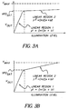
- the sensor output response will be as shown in Figures 3a and 3b.
- the output response comprises 2 regions.
- the output response will follow linear region 1.
- the number of photoelectrons exceeds the capacity of the photodetector, this charge will be collected on the floating diffusion and added to the photodetector signal charge.
- the pixel output response will follow region 2.
- the preferred embodiment provides a linear response in region 2, by the timing shown in Fig. 2a.
- a non-linear response could be generated by having a time varying reset gate potential level as described in the prior art reference by S.
- the output response in region 2 is linear, and the slope is dependent on and directly proportional to the floating diffusion integration time t intfd .
- the two Figures (3a and 3b) illustrate the 2 different slopes for region 2.
- the floating diffusion integration time in Fig. 3a is shorter than that for Fig 3b. Consequently, the slope of region 2 in Fig 3b. is greater than that for Fig. 3a.
- the effective signal level of the pixel can be determined by Equation 6.
- Veff Vout for Vout ⁇ Vpdsat
- Veff Vpdsat + (Vout - Vpdsat)(t pdint /t fdint ) for Vout > Vpdsat
- the ratio of the photodetector integration time t intpd to the floating diffusion integration time t intfd can be made large, Veff can be increased substantially over the signal limited by the photodetector capacity. Hence, the dynamic range is extended.
- Vmax which is determined by the floating diffusion charge capacity
- Vmax can be larger than that of the photodetector capacity by controlling the capacitance of the floating diffusion. It is also possible to display the sensor output signal directly without determining the effective signal level from region 2. This still provides extended instrascene dynamic range by mapping and directly displaying a larger incident illuminant range into the directly detectable signal voltage range. Also, the level of Vpdsat can be programmed by setting the off level of the transfer gate 16 to the desired level.
- Fig. 2a shows a single readout of the total combined charge on the floating diffusion that comprises the photodetector signal and the collected blooming charge.
- the signal is read first followed by a reset and then a measurement of the reset level. This is an uncorrelated double sample readout, which adds temporal reset noise to the signal. It is possible to accomplish readout of the photodetector signal level and floating diffusion blooming charge level by performing 2 readouts. This is shown in Fig 2b.
- the level of blooming charge collected on the floating diffusion 18 is sampled and held by pulsing SHS fd which places the blooming charge on Capacitor C 4 , followed by a reset of the floating diffusion 18 by RG and a sample and hold of the reset level by SHR which places the reset level on Capacitor C 5 .
- Charge is then transferred from the photodetector 12 to the floating diffusion 18 and that signal level is then sampled and held by SHS pd and placed on Capacitor C 6 .
- the present invention envisions a differential readout for the stored blooming charge on capacitor C 4 and the reset level on capacitor C 5 via differential amplifier 31, and a second differential readout for the stored signal charge on capacitor C 6 and the reset level on capacitor C 5 via differential amplifier 32, thus providing true correlated double sampling for the photodetector signal level.
- the final output signal can then be determined by several means. One is reading the signals from the 2 differential amplifiers 31 and 32 separately providing 2 signal values per pixel that can be added off-chip. A second embodiment is accomplished by providing the signals as inputs to a 3 rd differential amplifier and reading the signal out as a single level per pixel.
- This readout method of combining the signal in the voltage domain also provides a larger Vmax than combining the signals in the charge domain. This is because the floating diffusion does not have to hold the photodetector signal and blooming signal simultaneously. Hence the Vmax is extended to be the full floating diffusion capacity plus the photodetector capacity.
- the second embodiment of the present invention also utilizes blooming behavior to extend dynamic range.
- CMOS APS and PPS devices it is pointed out that as the incident light level becomes extremely bright, the output signal determined from the difference between the signal level and a reset level is perceived to decrease with increasing light levels, eventually reaching a "black" level.
- This diminishing signal behavior is due to the effect of the reset level decreasing as a result of charge accumulating on the charge to voltage conversion node, typically referred to as a sense node, during the time between reset and when the reset level is sampled and held.
- FIG. 5a and 7a Cross sectional diagrams of the relevant region of pixels envisioned to operate under the second embodiment of the present invention are shown schematically in Figs. 5a and 7a with corresponding timing diagrams of Figs. 4 and 6.
- the pixel 20 shown in Fig. 5a and the corresponding timing diagram of Figs. 4 are for the case of either a 3 transistor APS device where the photodetector serves as the charge to voltage conversion node, and also or for the case of a PPS device.
- the pixel 30 shown in Fig. 7a and the corresponding timing diagram of Figs. 6 are for the case of an APS where the charge to voltage conversion node (floating diffusion 38) is separate and isolated from the photodetector 32.
- the pixel 20 is initialized by resetting the photodetector 22 when RG 27 is pulsed on and off. Integration of signal in the photodetector now commences. As integration proceeds the electrostatic potential of the photodetector VPD decreases until the photodetector 22 has completely filled up with photoelectrons. At this point the VPD is approximately 0 volts. The signal level of the photodetector 22 is then sampled and held by strobing SHS. Next the photodetector is reset by strobing RG 27 in order to provided a reference level differential readout of the signal from photodetector 22.
- the time elapsed between the reset and sample and bold of the reset level is typically a few ⁇ sec. If the incident light level during this elapsed time is low, the reset level will not change appreciably and will be extremely close to the nominal reset level RL0 as shown in Fig. 5b. If this incident light is very bright, the reset level can change during this elapsed time if the sensor is not shielded from the incident light.
- the example seen in Fig. 5c is for a very bright incident light level that causes the photodetector voltage VPD to go to reset level RLA.
- the perceived output signal level will decrease because the full photodetector level is compared against RLA rather than RL0. If the incident light level is bright enough to completely fill the photodetector in the time between reset and sample and hold of the rest level, the photodetector will reach a reset level RLB as seen in Fig. 5d. In this case the difference between the sampled and held signal level and the sampled and held reset level is zero, producing a black or dark image. This produces a diminishing signal region with increasing incident light intensity as shown in Figs. 8a and 8b.
- Figs. 6 and 7a which is for the case of four transistor APS devices, the same effect occurs.
- the photodetector 32 fills up and excess electrons spill into the floating diffusion 38, consequently decreasing the reset level and the differentially read out signal level in a manner similar to that described for Fig. 4 and Figs. 5a through 5d.
- the transfer function is very linear and reaches a black level at incident light levels that are 20,000x to 50,000x the normal saturation exposure, Isat, as shown in Fig. 8b.
- the x-axis scale extends from no illumination to 3x times the saturation exposure. With this x-axis scale it is possible to discern the linear region output response of the pixel prior to saturation. This is the region between no illumination and Isat.
- the x-axis scale is changed in Fig 3b to extend from no illumination to 50,000 times Isat. With this scale it is easier to discern the output response of the sensor in the saturated region, but difficult to discern the region prior to saturation shown in Fig. 3a.
- the output signal diminishes linearly, or by some other characterized and empirically known transfer function, until reaching ⁇ 50,000 times Isat, where the output signal reaches 0 volts and appears as a black or dark signal.
- the new concept presented with the present invention is to use this diminishing signal region to determine the "effective signal level” to extend dynamic range.
- the "effective reset integration time” for this behavior is simply elapsed time between the falling edge of the reset of the charge to voltage conversion node and the falling edge of the sample and hold of the reset level, as shown in Fig. 4 and Fig. 6.
- the signal change in this small integration time can be ascertained by having two reset sequences that are sampled and held with different effective integration times. If there is a difference between the 2 reset levels that exceed a predetermined threshold, then it is known that pixel is in the diminishing signal region of the response curve. This could also be done by comparing a single reset level to a reference reset level that is generated from a dark reset.
- the incident illumination level can be determined from the specific measured transfer function provided by the diminishing signal region of the sensor.
- incident illumination levels from no illumination up to 50,000x the saturation exposure can be detected by the sensor, providing extended dynamic range.
- a comparator with a programmable threshold is used to determine if there is a difference between the 2 reset levels with different elapsed times between reset and sample and hold of the reset level.
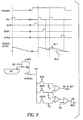
- the pixel output signal level is read in a manner similar to that described in prior art; the sampled and held photodetector signal level is read out differentially with respect to reset1, and digitized to N bits, (8 shown in this example).
- the output of this comparator with reset1 and reset2 as inputs is then used as a transfer function bit.
- a "zero" transfer function bit indicates that the 8 bit photodetector signal level should be used as is.
- a "one" transfer function bit indicates that the 8 bit photodetector signal level should be calculated using the 8 bit output using the saturated region transfer function.
- the timing for this readout operation is also shown in Fig. 9 for the pixel shown in Fig. 5a.
- the floating diffusion is reset and the reset level is sampled and held. This is reset1 and has an elapsed reset integration time 1.
- the charge in the PD is transferred to the floating diffusion and the signal level is sampled and held.
- the FD is reset and the reset level is sampled and held provided reset2, with an elapsed reset integration time 2 that is different than that for reset1.
- the actual value of the differences in reset levels could be read out in a similar manner to that used to determine the value of (signal-reset1).
- This value of (reset2-reset1) could then be used to determine the effective signal level using equation 7.
- a comparison could be done to provide a flag bit to determine which value, either signal-reset1, or reset2-reset1 to read out through the 8 bit ADC.
Landscapes
- Engineering & Computer Science (AREA)
- Multimedia (AREA)
- Signal Processing (AREA)
- Solid State Image Pick-Up Elements (AREA)
- Transforming Light Signals Into Electric Signals (AREA)
Abstract
Description


Claims (10)
- A X-Y addressable MOS imager sensor comprising:a semiconductor based MOS sensor having an array of pixels forming the X-Y addressable MOS imager, the X-Y addressable MOS imager having a plurality of the pixels such that each pixel within the plurality of pixels has a photodetector with a reset mechanism that adjusts the photodetector potential to a predetermined potential level;means for measuring a plurality of reset levels with two different elapsed times between reset and measurement of the reset level;a comparison circuit operatively coupled to the means for measuring to determine a difference in reset levels;a predetermined set of transfer functions used to identify effective signal levels of the photodetectors;means for determining from the difference which transfer function is applicable to that photodetector range of accumulated light; andmeans responsive to the means for determining for applying the transfer function to the charge read out from the photodetector.
- The invention of claim 1 wherein the predetermined set of transfer functions further comprises at least a first transfer function that is pre-photodetector saturation function and a second transfer function that is a post-photodetector saturation transfer function.
- The invention of claim 2 wherein the means for measuring further comprises means for measuring two reset levels of the photodetector within the same row readout period.
- The invention of claim 2 wherein means responsive further comprises means for applying a series of digital adds and digital multiplies.
- The invention of claim 1 wherein the comparison means compares the different reset periods with respect to a predetermined threshold.
- The invention of claim 1 wherein the means for measuring further comprises means for measuring the difference between the 2 reset levels and using this difference to calculate the effective pixel signal level.
- A method of using an X-Y addressable MOS imager sensor for increased dynamic range comprising the steps of:providing as the X-Y imager a semiconductor based image sensor having an array of pixels formed in rows and columns such with a plurality of the pixels formed such that each pixel within the plurality of pixels has a photodetector with a reset mechanism that adjusts the photodetector potential to a predetermined potential level;measuring a plurality of reset levels for each of the plurality of pixels with two different elapsed times between reset and measurement of the reset level;comparing the measured reset levels to determine a difference in the reset levels;applying a predetermined set of transfer functions to the difference;determining from the applying step amount of light incident upon the photodetector.
- The method of claim 15 wherein the applying step further comprises applying a first transfer function that is pre-photodetector saturation function and a second transfer function that is a post-photodetector saturation transfer function.
- The method of claim 15 wherein the measuring step further comprises measuring two reset levels of the photodetector within the same frame time period.
- The method of claim 15 wherein the determining step further comprises applying a series of digital adds and digital multiplies.
Applications Claiming Priority (2)
| Application Number | Priority Date | Filing Date | Title |
|---|---|---|---|
| US09/426,870 US6486504B1 (en) | 1999-10-26 | 1999-10-26 | CMOS image sensor with extended dynamic range |
| US426870 | 1999-10-26 |
Publications (3)
| Publication Number | Publication Date |
|---|---|
| EP1096789A2 true EP1096789A2 (en) | 2001-05-02 |
| EP1096789A3 EP1096789A3 (en) | 2003-03-26 |
| EP1096789B1 EP1096789B1 (en) | 2011-12-28 |
Family
ID=23692547
Family Applications (1)
| Application Number | Title | Priority Date | Filing Date |
|---|---|---|---|
| EP00203610A Expired - Lifetime EP1096789B1 (en) | 1999-10-26 | 2000-10-17 | Cmos image sensor with extended dynamic range |
Country Status (4)
| Country | Link |
|---|---|
| US (2) | US6486504B1 (en) |
| EP (1) | EP1096789B1 (en) |
| JP (1) | JP4536901B2 (en) |
| KR (1) | KR100657103B1 (en) |
Cited By (4)
| Publication number | Priority date | Publication date | Assignee | Title |
|---|---|---|---|---|
| EP1349379A3 (en) * | 2002-03-27 | 2004-01-02 | Omnivision Technologies Inc. | Method and apparatus for thermal noise canceling in a linear CMOS image sensor |
| EP1458179A3 (en) * | 2003-03-13 | 2006-04-12 | Eastman Kodak Company | A system with a random number generator used to remove contouring in CMOS imager data having an extended dynamic range |
| US7583305B2 (en) | 2004-07-07 | 2009-09-01 | Eastman Kodak Company | Extended dynamic range imaging system |
| WO2010071696A1 (en) | 2008-12-17 | 2010-06-24 | Sony Computer Entertainment Inc. | Compensating for blooming of a shape in an image |
Families Citing this family (105)
| Publication number | Priority date | Publication date | Assignee | Title |
|---|---|---|---|---|
| US7023479B2 (en) * | 2000-05-16 | 2006-04-04 | Canon Kabushiki Kaisha | Image input apparatus having addition and subtraction processing |
| JP3827145B2 (en) * | 2001-07-03 | 2006-09-27 | ソニー株式会社 | Solid-state imaging device |
| US20060061008A1 (en) | 2004-09-14 | 2006-03-23 | Lee Karner | Mounting assembly for vehicle interior mirror |
| US7623645B1 (en) * | 2002-07-23 | 2009-11-24 | At&T Intellectual Property, I, L.P. | System and method for gathering information related to a geographical location of a caller in a public switched telephone network |
| US7583826B2 (en) * | 2002-07-31 | 2009-09-01 | Casio Computer Co., Ltd. | Image reading apparatus and its driving method |
| NL1023440C2 (en) * | 2003-05-16 | 2004-11-17 | Univ Amsterdam | Method and device for forming an image of an object. |
| US7859581B2 (en) * | 2003-07-15 | 2010-12-28 | Eastman Kodak Company | Image sensor with charge binning and dual channel readout |
| US6900484B2 (en) * | 2003-07-30 | 2005-05-31 | Micron Technology, Inc. | Angled pinned photodiode for high quantum efficiency |
| WO2005015639A1 (en) * | 2003-08-12 | 2005-02-17 | Simon Fraser University | Multi-mode digital imaging apparatus and system |
| US7830435B2 (en) * | 2003-09-03 | 2010-11-09 | Eastman Kodak Company | Image sensor and image capture system with extended dynamic range |
| US20050083421A1 (en) * | 2003-10-16 | 2005-04-21 | Vladimir Berezin | Dynamic range enlargement in CMOS image sensors |
| US20050128327A1 (en) * | 2003-12-10 | 2005-06-16 | Bencuya Selim S. | Device and method for image sensing |
| US7446812B2 (en) | 2004-01-13 | 2008-11-04 | Micron Technology, Inc. | Wide dynamic range operations for imaging |
| JP4502278B2 (en) * | 2004-02-27 | 2010-07-14 | 国立大学法人東北大学 | Solid-state imaging device, line sensor, optical sensor, and operation method of solid-state imaging device |
| CN100499146C (en) * | 2004-02-27 | 2009-06-10 | 国立大学法人东北大学 | Solid-state imagine device, line sensor, optical sensor |
| US6873282B1 (en) | 2004-03-04 | 2005-03-29 | Charles Douglas Murphy | Differential time-to-threshold A/D conversion in digital imaging arrays |
| US7126512B2 (en) * | 2004-03-19 | 2006-10-24 | Charles Douglas Murphy | Comparing circuits for time-to-threshold A/D conversion in digital imaging arrays |
| JP4317115B2 (en) * | 2004-04-12 | 2009-08-19 | 国立大学法人東北大学 | Solid-state imaging device, optical sensor, and operation method of solid-state imaging device |
| CN100525401C (en) * | 2004-04-12 | 2009-08-05 | 国立大学法人东北大学 | Solid-state imaging device, optical sensor, and solid-state imaging device operation method |
| US7643693B1 (en) | 2004-04-16 | 2010-01-05 | Apple Inc. | Fast lossless encoder for digitized analog data |
| US7751475B1 (en) | 2004-06-22 | 2010-07-06 | Apple Inc. | Arbitrary-resolution, extreme-quality video codec |
| US7397509B2 (en) * | 2004-08-27 | 2008-07-08 | Micron Technology, Inc. | High dynamic range imager with a rolling shutter |
| CA2494602A1 (en) * | 2005-01-08 | 2006-07-08 | Karim S. Karim | Digital imaging apparatus and system |
| US7616231B2 (en) * | 2005-01-06 | 2009-11-10 | Goodrich Corporation | CMOS active pixel sensor with improved dynamic range and method of operation for object motion detection |
| US7551059B2 (en) * | 2005-01-06 | 2009-06-23 | Goodrich Corporation | Hybrid infrared detector array and CMOS readout integrated circuit with improved dynamic range |
| US7518645B2 (en) * | 2005-01-06 | 2009-04-14 | Goodrich Corp. | CMOS active pixel sensor with improved dynamic range and method of operation |
| US7916186B2 (en) | 2005-04-07 | 2011-03-29 | Micron Technology, Inc. | Anti-eclipse circuitry with tracking of floating diffusion reset level |
| JP2006294871A (en) * | 2005-04-11 | 2006-10-26 | Matsushita Electric Ind Co Ltd | Solid-state imaging device |
| US7282685B2 (en) * | 2005-04-14 | 2007-10-16 | Micron Technology, Inc. | Multi-point correlated sampling for image sensors |
| JP2007036425A (en) * | 2005-07-25 | 2007-02-08 | Pentax Corp | Analog device drive system and imaging apparatus |
| US20070040922A1 (en) * | 2005-08-22 | 2007-02-22 | Micron Technology, Inc. | HDR/AB on multi-way shared pixels |
| JP2007097127A (en) * | 2005-08-30 | 2007-04-12 | Konica Minolta Holdings Inc | Solid-state imaging device |
| KR100804495B1 (en) * | 2005-11-04 | 2008-02-20 | (주) 픽셀플러스 | Black solar phenomenon suppression apparatus and method of CMOS image sensor |
| US7633106B2 (en) * | 2005-11-09 | 2009-12-15 | International Business Machines Corporation | Light shield for CMOS imager |
| US7671460B2 (en) * | 2006-01-25 | 2010-03-02 | Teledyne Licensing, Llc | Buried via technology for three dimensional integrated circuits |
| US8698894B2 (en) | 2006-02-07 | 2014-04-15 | Magna Electronics Inc. | Camera mounted at rear of vehicle |
| EP1845706A1 (en) * | 2006-04-12 | 2007-10-17 | CSEM Centre Suisse d'Electronique et de Microtechnique SA | Photo sensor with pinned photodiode and sub-linear response |
| JP4948089B2 (en) * | 2006-08-25 | 2012-06-06 | キヤノン株式会社 | Imaging apparatus and control method thereof |
| US7923763B2 (en) * | 2007-03-08 | 2011-04-12 | Teledyne Licensing, Llc | Two-dimensional time delay integration visible CMOS image sensor |
| US7674648B2 (en) * | 2007-03-21 | 2010-03-09 | Eastman Kodak Company | Extended dynamic range using variable sensitivity pixels |
| US7924332B2 (en) * | 2007-05-25 | 2011-04-12 | The Trustees Of The University Of Pennsylvania | Current/voltage mode image sensor with switchless active pixels |
| US8199236B2 (en) * | 2007-09-11 | 2012-06-12 | Simon Fraser University/Industry Liason Office | Device and pixel architecture for high resolution digital |
| US7920193B2 (en) * | 2007-10-23 | 2011-04-05 | Aptina Imaging Corporation | Methods, systems and apparatuses using barrier self-calibration for high dynamic range imagers |
| JP5142680B2 (en) * | 2007-11-19 | 2013-02-13 | キヤノン株式会社 | Photoelectric conversion device and imaging system |
| JP5127467B2 (en) * | 2008-01-07 | 2013-01-23 | キヤノン株式会社 | IMAGING SYSTEM AND IMAGING SYSTEM CONTROL METHOD |
| US7795650B2 (en) * | 2008-12-09 | 2010-09-14 | Teledyne Scientific & Imaging Llc | Method and apparatus for backside illuminated image sensors using capacitively coupled readout integrated circuits |
| JP5805636B2 (en) | 2010-06-24 | 2015-11-04 | Hoya株式会社 | Magnetic recording medium |
| US8466402B2 (en) | 2010-10-25 | 2013-06-18 | Aptina Imaging Corporation | Imaging pixels with shielded floating diffusions |
| US9264672B2 (en) | 2010-12-22 | 2016-02-16 | Magna Mirrors Of America, Inc. | Vision display system for vehicle |
| JP5361938B2 (en) * | 2011-05-02 | 2013-12-04 | キヤノン株式会社 | Solid-state imaging device and camera |
| KR101930755B1 (en) | 2012-03-21 | 2018-12-19 | 삼성전자주식회사 | Method of driving an image sensor |
| US9337223B2 (en) | 2013-11-25 | 2016-05-10 | Semiconductor Components Industriess, Llc | Imaging systems with image pixels having adjustable responsivity |
| US9526468B2 (en) | 2014-09-09 | 2016-12-27 | General Electric Company | Multiple frame acquisition for exposure control in X-ray medical imagers |
| US10163948B2 (en) * | 2015-07-23 | 2018-12-25 | Semiconductor Energy Laboratory Co., Ltd. | Imaging device and electronic device |
| US11297258B2 (en) * | 2015-10-01 | 2022-04-05 | Qualcomm Incorporated | High dynamic range solid state image sensor and camera system |
| CN107306344B (en) * | 2016-04-20 | 2021-02-26 | 格科微电子(上海)有限公司 | Method for realizing high dynamic range image sensor |
| US10917625B1 (en) | 2016-10-20 | 2021-02-09 | Facebook Technologies, Llc | Time multiplexed dual-band sensor |
| US10917589B2 (en) * | 2017-06-26 | 2021-02-09 | Facebook Technologies, Llc | Digital pixel with extended dynamic range |
| US10686996B2 (en) | 2017-06-26 | 2020-06-16 | Facebook Technologies, Llc | Digital pixel with extended dynamic range |
| US10419701B2 (en) | 2017-06-26 | 2019-09-17 | Facebook Technologies, Llc | Digital pixel image sensor |
| US11568609B1 (en) | 2017-07-25 | 2023-01-31 | Meta Platforms Technologies, Llc | Image sensor having on-chip compute circuit |
| US10726627B2 (en) | 2017-07-25 | 2020-07-28 | Facebook Technologies, Llc | Sensor system based on stacked sensor layers |
| US10825854B2 (en) | 2017-08-16 | 2020-11-03 | Facebook Technologies, Llc | Stacked photo sensor assembly with pixel level interconnect |
| US10598546B2 (en) | 2017-08-17 | 2020-03-24 | Facebook Technologies, Llc | Detecting high intensity light in photo sensor |
| US11393867B2 (en) | 2017-12-06 | 2022-07-19 | Facebook Technologies, Llc | Multi-photodiode pixel cell |
| US11057581B2 (en) | 2018-01-24 | 2021-07-06 | Facebook Technologies, Llc | Digital pixel array with multi-stage readouts |
| US10827142B2 (en) | 2018-03-02 | 2020-11-03 | Facebook Technologies, Llc | Digital pixel array with adaptive exposure |
| US10969273B2 (en) | 2018-03-19 | 2021-04-06 | Facebook Technologies, Llc | Analog-to-digital converter having programmable quantization resolution |
| US10553180B1 (en) | 2018-03-21 | 2020-02-04 | Facebook Technologies, Llc | Dynamically structured protective film for maximum display resolution |
| US11054632B1 (en) | 2018-03-21 | 2021-07-06 | Facebook Technologies, Llc | Liquid filled pixelated film |
| US11004881B2 (en) | 2018-04-03 | 2021-05-11 | Facebook Technologies, Llc | Global shutter image sensor |
| US10923523B2 (en) * | 2018-04-16 | 2021-02-16 | Facebook Technologies, Llc | Multi-photodiode pixel cell |
| US10848681B2 (en) | 2018-04-17 | 2020-11-24 | Facebook Technologies, Llc | Image reconstruction from image sensor output |
| US10685594B2 (en) | 2018-05-08 | 2020-06-16 | Facebook Technologies, Llc | Calibrating brightness variation in a display |
| US11233085B2 (en) | 2018-05-09 | 2022-01-25 | Facebook Technologies, Llc | Multi-photo pixel cell having vertical gate structure |
| US12034015B2 (en) | 2018-05-25 | 2024-07-09 | Meta Platforms Technologies, Llc | Programmable pixel array |
| US10804926B2 (en) | 2018-06-08 | 2020-10-13 | Facebook Technologies, Llc | Charge leakage compensation in analog-to-digital converter |
| US11089241B2 (en) | 2018-06-11 | 2021-08-10 | Facebook Technologies, Llc | Pixel cell with multiple photodiodes |
| US11906353B2 (en) | 2018-06-11 | 2024-02-20 | Meta Platforms Technologies, Llc | Digital pixel with extended dynamic range |
| US11089210B2 (en) | 2018-06-11 | 2021-08-10 | Facebook Technologies, Llc | Configurable image sensor |
| US11463636B2 (en) | 2018-06-27 | 2022-10-04 | Facebook Technologies, Llc | Pixel sensor having multiple photodiodes |
| US10897586B2 (en) | 2018-06-28 | 2021-01-19 | Facebook Technologies, Llc | Global shutter image sensor |
| US10931884B2 (en) | 2018-08-20 | 2021-02-23 | Facebook Technologies, Llc | Pixel sensor having adaptive exposure time |
| US11956413B2 (en) | 2018-08-27 | 2024-04-09 | Meta Platforms Technologies, Llc | Pixel sensor having multiple photodiodes and shared comparator |
| US11595602B2 (en) | 2018-11-05 | 2023-02-28 | Meta Platforms Technologies, Llc | Image sensor post processing |
| US11102430B2 (en) | 2018-12-10 | 2021-08-24 | Facebook Technologies, Llc | Pixel sensor having multiple photodiodes |
| US11962928B2 (en) | 2018-12-17 | 2024-04-16 | Meta Platforms Technologies, Llc | Programmable pixel array |
| US11888002B2 (en) | 2018-12-17 | 2024-01-30 | Meta Platforms Technologies, Llc | Dynamically programmable image sensor |
| US11218660B1 (en) | 2019-03-26 | 2022-01-04 | Facebook Technologies, Llc | Pixel sensor having shared readout structure |
| US11943561B2 (en) | 2019-06-13 | 2024-03-26 | Meta Platforms Technologies, Llc | Non-linear quantization at pixel sensor |
| US12108141B2 (en) | 2019-08-05 | 2024-10-01 | Meta Platforms Technologies, Llc | Dynamically programmable image sensor |
| US11936998B1 (en) | 2019-10-17 | 2024-03-19 | Meta Platforms Technologies, Llc | Digital pixel sensor having extended dynamic range |
| US11935291B2 (en) | 2019-10-30 | 2024-03-19 | Meta Platforms Technologies, Llc | Distributed sensor system |
| US11948089B2 (en) | 2019-11-07 | 2024-04-02 | Meta Platforms Technologies, Llc | Sparse image sensing and processing |
| US12141888B1 (en) | 2019-12-18 | 2024-11-12 | Meta Platforms Technologies, Llc | Dynamic and hierarchical image sensing and processing |
| US11902685B1 (en) | 2020-04-28 | 2024-02-13 | Meta Platforms Technologies, Llc | Pixel sensor having hierarchical memory |
| US11825228B2 (en) | 2020-05-20 | 2023-11-21 | Meta Platforms Technologies, Llc | Programmable pixel array having multiple power domains |
| US11910114B2 (en) | 2020-07-17 | 2024-02-20 | Meta Platforms Technologies, Llc | Multi-mode image sensor |
| US12075175B1 (en) | 2020-09-08 | 2024-08-27 | Meta Platforms Technologies, Llc | Programmable smart sensor with adaptive readout |
| US11956560B2 (en) | 2020-10-09 | 2024-04-09 | Meta Platforms Technologies, Llc | Digital pixel sensor having reduced quantization operation |
| US11935575B1 (en) | 2020-12-23 | 2024-03-19 | Meta Platforms Technologies, Llc | Heterogeneous memory system |
| US12022218B2 (en) | 2020-12-29 | 2024-06-25 | Meta Platforms Technologies, Llc | Digital image sensor using a single-input comparator based quantizer |
| US12244936B2 (en) | 2022-01-26 | 2025-03-04 | Meta Platforms Technologies, Llc | On-sensor image processor utilizing contextual data |
| US12598402B2 (en) | 2023-07-16 | 2026-04-07 | Apple Inc. | Partial pixel oversampling for high dynamic range imaging |
| US12610163B2 (en) * | 2023-12-14 | 2026-04-21 | Apple Inc. | Low-power/small-area current-mode pixel readout circuit |
Family Cites Families (6)
| Publication number | Priority date | Publication date | Assignee | Title |
|---|---|---|---|---|
| JP2953297B2 (en) | 1994-03-30 | 1999-09-27 | 日本電気株式会社 | Light receiving element and driving method thereof |
| JP3680366B2 (en) * | 1995-08-11 | 2005-08-10 | ソニー株式会社 | Imaging device |
| JP2992012B2 (en) * | 1997-07-28 | 1999-12-20 | 松下電子工業株式会社 | Amplification type solid-state imaging device, driving method thereof, and physical quantity distribution detecting semiconductor device |
| US6008486A (en) * | 1997-12-31 | 1999-12-28 | Gentex Corporation | Wide dynamic range optical sensor |
| JP3903361B2 (en) * | 1999-08-13 | 2007-04-11 | 日本放送協会 | Solid-state imaging device |
| US6307195B1 (en) * | 1999-10-26 | 2001-10-23 | Eastman Kodak Company | Variable collection of blooming charge to extend dynamic range |
-
1999
- 1999-10-26 US US09/426,870 patent/US6486504B1/en not_active Expired - Lifetime
-
2000
- 2000-10-17 EP EP00203610A patent/EP1096789B1/en not_active Expired - Lifetime
- 2000-10-20 JP JP2000320507A patent/JP4536901B2/en not_active Expired - Lifetime
- 2000-10-25 KR KR1020000062901A patent/KR100657103B1/en not_active Expired - Lifetime
-
2002
- 2002-09-06 US US10/236,826 patent/US6680498B2/en not_active Expired - Lifetime
Cited By (10)
| Publication number | Priority date | Publication date | Assignee | Title |
|---|---|---|---|---|
| EP1349379A3 (en) * | 2002-03-27 | 2004-01-02 | Omnivision Technologies Inc. | Method and apparatus for thermal noise canceling in a linear CMOS image sensor |
| CN1306791C (en) * | 2002-03-27 | 2007-03-21 | 全视技术有限公司 | Method and appts. of eliminating KTC noise in linear CMOS imaging sensor |
| EP1919192A3 (en) * | 2002-03-27 | 2009-05-13 | Omnivision Technologies Inc. | Method and apparatus for kTC noise canceling in a linear CMOS image sensor |
| EP1458179A3 (en) * | 2003-03-13 | 2006-04-12 | Eastman Kodak Company | A system with a random number generator used to remove contouring in CMOS imager data having an extended dynamic range |
| US7349126B2 (en) | 2003-03-13 | 2008-03-25 | Eastman Kodak Company | System with a random number generator used to remove contouring in CMOS imager data having an extended dynamic range |
| US7643177B2 (en) | 2003-03-13 | 2010-01-05 | Eastman Kodak Company | System with a random number generator used to remove contouring in CMOS imager data having an extended dynamic range |
| US7583305B2 (en) | 2004-07-07 | 2009-09-01 | Eastman Kodak Company | Extended dynamic range imaging system |
| WO2010071696A1 (en) | 2008-12-17 | 2010-06-24 | Sony Computer Entertainment Inc. | Compensating for blooming of a shape in an image |
| EP2359312A4 (en) * | 2008-12-17 | 2013-01-16 | Sony Computer Entertainment Inc | COMPENSATION FOR HYPERLUMINOSITY OF A SHAPE IN AN IMAGE |
| US8970707B2 (en) | 2008-12-17 | 2015-03-03 | Sony Computer Entertainment Inc. | Compensating for blooming of a shape in an image |
Also Published As
| Publication number | Publication date |
|---|---|
| JP4536901B2 (en) | 2010-09-01 |
| US6486504B1 (en) | 2002-11-26 |
| US20030020100A1 (en) | 2003-01-30 |
| US6680498B2 (en) | 2004-01-20 |
| EP1096789A3 (en) | 2003-03-26 |
| KR100657103B1 (en) | 2006-12-12 |
| JP2001169184A (en) | 2001-06-22 |
| KR20010060209A (en) | 2001-07-06 |
| EP1096789B1 (en) | 2011-12-28 |
Similar Documents
| Publication | Publication Date | Title |
|---|---|---|
| EP1096790B1 (en) | Variable collection of blooming charge to extend dynamic range | |
| EP1096789B1 (en) | Cmos image sensor with extended dynamic range | |
| US6069377A (en) | Image sensor incorporating saturation time measurement to increase dynamic range | |
| US7920193B2 (en) | Methods, systems and apparatuses using barrier self-calibration for high dynamic range imagers | |
| EP1119188B1 (en) | Cmos active pixel image sensor with extended dynamic range and sensitivity | |
| US7468501B2 (en) | Linear dynamic range enhancement in a CMOS imager | |
| JP4315032B2 (en) | Solid-state imaging device and driving method of solid-state imaging device | |
| US7768563B2 (en) | Method and circuit for determining the response curve knee point in active pixel image sensors with extended dynamic range | |
| EP1475961A1 (en) | Combined linear-logarithmic image sensor | |
| JP3927696B2 (en) | Imaging device | |
| US8063963B2 (en) | Imaging device having a pixel structure with high dynamic range read-out signal | |
| EP1233612B1 (en) | CMOS image sensor with extended dynamic range | |
| US20030227018A1 (en) | Five transistor CMOS pixel | |
| US7106373B1 (en) | Method for increasing dynamic range of a pixel by multiple incomplete reset | |
| Pain | Linear dynamic range enhancement in a CMOS imager |
Legal Events
| Date | Code | Title | Description |
|---|---|---|---|
| PUAI | Public reference made under article 153(3) epc to a published international application that has entered the european phase |
Free format text: ORIGINAL CODE: 0009012 |
|
| AK | Designated contracting states |
Kind code of ref document: A2 Designated state(s): AT BE CH CY DE DK ES FI FR GB GR IE IT LI LU MC NL PT SE |
|
| AX | Request for extension of the european patent |
Free format text: AL;LT;LV;MK;RO;SI |
|
| PUAL | Search report despatched |
Free format text: ORIGINAL CODE: 0009013 |
|
| AK | Designated contracting states |
Kind code of ref document: A3 Designated state(s): AT BE CH CY DE DK ES FI FR GB GR IE IT LI LU MC NL PT SE |
|
| AX | Request for extension of the european patent |
Extension state: AL LT LV MK RO SI |
|
| 17P | Request for examination filed |
Effective date: 20030818 |
|
| AKX | Designation fees paid |
Designated state(s): DE FR GB NL |
|
| 17Q | First examination report despatched |
Effective date: 20060316 |
|
| REG | Reference to a national code |
Ref country code: DE Ref legal event code: R079 Ref document number: 60046785 Country of ref document: DE Free format text: PREVIOUS MAIN CLASS: H04N0003150000 Ipc: H04N0005355000 |
|
| GRAP | Despatch of communication of intention to grant a patent |
Free format text: ORIGINAL CODE: EPIDOSNIGR1 |
|
| RIC1 | Information provided on ipc code assigned before grant |
Ipc: H04N 5/355 20110101AFI20110527BHEP Ipc: H04N 5/3745 20110101ALI20110527BHEP |
|
| RAP1 | Party data changed (applicant data changed or rights of an application transferred) |
Owner name: OMNIVISION TECHNOLOGIES, INC. |
|
| GRAS | Grant fee paid |
Free format text: ORIGINAL CODE: EPIDOSNIGR3 |
|
| GRAA | (expected) grant |
Free format text: ORIGINAL CODE: 0009210 |
|
| AK | Designated contracting states |
Kind code of ref document: B1 Designated state(s): DE FR GB NL |
|
| REG | Reference to a national code |
Ref country code: GB Ref legal event code: FG4D |
|
| REG | Reference to a national code |
Ref country code: DE Ref legal event code: R096 Ref document number: 60046785 Country of ref document: DE Effective date: 20120308 |
|
| REG | Reference to a national code |
Ref country code: NL Ref legal event code: VDEP Effective date: 20111228 |
|
| PG25 | Lapsed in a contracting state [announced via postgrant information from national office to epo] |
Ref country code: NL Free format text: LAPSE BECAUSE OF FAILURE TO SUBMIT A TRANSLATION OF THE DESCRIPTION OR TO PAY THE FEE WITHIN THE PRESCRIBED TIME-LIMIT Effective date: 20111228 |
|
| PLBE | No opposition filed within time limit |
Free format text: ORIGINAL CODE: 0009261 |
|
| STAA | Information on the status of an ep patent application or granted ep patent |
Free format text: STATUS: NO OPPOSITION FILED WITHIN TIME LIMIT |
|
| 26N | No opposition filed |
Effective date: 20121001 |
|
| REG | Reference to a national code |
Ref country code: DE Ref legal event code: R097 Ref document number: 60046785 Country of ref document: DE Effective date: 20121001 |
|
| REG | Reference to a national code |
Ref country code: FR Ref legal event code: PLFP Year of fee payment: 17 |
|
| REG | Reference to a national code |
Ref country code: FR Ref legal event code: PLFP Year of fee payment: 18 |
|
| REG | Reference to a national code |
Ref country code: FR Ref legal event code: PLFP Year of fee payment: 19 |
|
| PGFP | Annual fee paid to national office [announced via postgrant information from national office to epo] |
Ref country code: FR Payment date: 20190924 Year of fee payment: 20 |
|
| PGFP | Annual fee paid to national office [announced via postgrant information from national office to epo] |
Ref country code: GB Payment date: 20190925 Year of fee payment: 20 |
|
| PGFP | Annual fee paid to national office [announced via postgrant information from national office to epo] |
Ref country code: DE Payment date: 20190917 Year of fee payment: 20 |
|
| REG | Reference to a national code |
Ref country code: DE Ref legal event code: R071 Ref document number: 60046785 Country of ref document: DE |
|
| REG | Reference to a national code |
Ref country code: GB Ref legal event code: PE20 Expiry date: 20201016 |
|
| PG25 | Lapsed in a contracting state [announced via postgrant information from national office to epo] |
Ref country code: GB Free format text: LAPSE BECAUSE OF EXPIRATION OF PROTECTION Effective date: 20201016 |